ZW8P16LED Display Screen
Shenzhen ERALED Optoelectronics Co., Ltd.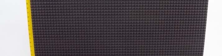
Click to zoom
Application Details
- Equipment Class
- JBC - Part 15 Class B Computing Device/Personal Computer
- Date of Grant
- Sep 12, 2011
- Application Purpose
- Original Equipment
- Date of Application
- Sep 12, 2011
- Equipment Note
- LED Display Screen
- Country
- China
Documents & Files
Document Text
Text extracted from the exhibit documents filed with the FCC. Open a document above to read the original.
Users Manual
Specification of the control system 一、Components description 1、The sending card ① DVI input ,connected to the DVI output of the graphics card. ② Serial por,connected to the serial port interface of the computer(RS232). ③ DIP interface,DC 5V power input. ④ 1U cable output,At output port 1. ⑤ 1D cable output,At output port 2. ⑥ Indicating lights of the power,the red light on for power up. ⑦ Signal light,the green light on after the signal being inputed. ⑧ DIP interface,DC 5V power input. ⑨ DIP interface,DC 5V power input. 2、The receiver card ① B-signal output or input. ② A-signal output of input. ③ DC 5V input. ④ Automatic inspection,the inspection button when there’s no signal. ⑤ Signal lights,the green light flashing after signal input. ⑥ The indicating lights of power,the red light on for DC 5v power up. ⑦ HUB interface,connect the screen to the conversion card with the same signal. ⑧ HUB interface,connect the screen to the conversion card with the same signal. 3、The graphics card ① DVI output,signal transmitted to the sending card 801. ② VGA output,signal transmitted to the display. 1、The Front Exploded View 256mm LED Lamp Display Surface Of The Cell Board Veil Point Spacing16mm 128mm 2、The Back Exploded View LED Drive IC 16P Signal Input Row Needle 16P Signal Output Connected Row Needle PCB Bottom Rind Screw Hole 1、The Front Exploded View Moudle Cabinet 1024mm 2、The Back Exploded View Signal in Signal out Positioning hole Power in Power out door lock Handle 3、The Back Door Open Exploded View Power line Signal line screw Connecting every cabinet and the order is as follows: Power Receiver card Handle Screen fixing frame After fixing one cabinet Lock for connecting with each cabinet Screen back 2、Power and signal connection 1):Connecting the power line for screen well, as shown in below. Screen Back 2):Connecting the signal line for screen well, as shown in below.。 Screen Back 3):Connecting screen power (input line) and network cable (signal input): Screen Back 3、Graphic card,Sending Card installation and setup Operating Environment Operating system Chinese/English Windows98/me/2000/NT/XP Hardware Configuration Pentium 300MHz or above ROM: 64M Graphics Card: Standard VGA 256mode or above Related Software Microsoft Media player compulsory OFFICE2000—in case of *. doc files RealPlayer—in case of RealPlayer files Operation steps: 1、 Put graphic card with DVI output into motherboard slot before starting PC Sending card Graphic card with DUI output DVI LINE RS232 LINE Moudle Cabinet Screen 2、 Turn on PC 3、 Enter graphic card installation directory, and then choose the correspondent graphic card drive, and then double click to install it according to the instruction. 4、 After finish the installation, please close the PC by hand. 5、 After closing the PC, please put the sending card into PCI slot in motherboard.(Please don’t use the DVI cable to connect Sending card with graphic card before starting the PC.) 6、 Turn on PC 7、 Connecting sending card with graphic card through DVI cable, and combining sending card with PC serial port through serial cable (RS232) DVI port DVI port Serial port RS232 cable DVI cable Connect monitor 二、Graphics card setup 1、If you want to install the ATI graphics card , please click“SETUP” Double click “setup”begin setup 2; After the intallation is completed,click“catalyst control center” setup done Double click”catalyst control center” 3、Select the baqsic/simple setup wizard choice “Basic{Easy Setup wizards and Quick Settings} Click Next to continue 4, The fourth: setup my display configuration Click “Go” to continue 5、The five i).Available Display Devices: Choose main display Click “Analog Monitor”{Lcd-Monitar} Click “Digital Flat Panel”{Led 1027x768} Click “Next” to continue The six 6、Select a Desktop Mode Click :Clone”{Current Mode} Click “Next” to continue The Seven 7、Display Setings for Desktop Viewing Desktop 1 is the main adapter(open:using and the main adapter),drag desktop 2 to the right Of desktop 1. Main: Lcd-Mantior And Clone:Led 1024x768 Desktop Area:1024x768 Click “Finish” to Succeed A、monitor management Desktop 1 (start-up( √)、maim monitor( √)) B、Desktop and monitor setup Desktop 1 + Desktop 2 Click “OK” to continue 8 8、A、Display manager Desktop and Display setup : { main+copy} 2 start-up( √) B、Desktop2 monitor setup Led 1024x768 {Expland} color {32bit} reftesh rate {60HZ} C、Click “OK” to continue 三、 LED studio installation 1). Please insert Led studio CD into PC CD-COM, and will pop-up installation dialog box. (If no dialog box pop-up, please double click the CD after select it.) As shown in below figure 4-1. Figure 4-1 2).Choose “Install Led studio” to start installation guidance, as shown in below figure 4-2. And the serial no. is 888888. Figure 4-2 3. After “LED Studio” software has been successfully installed, there will be a “LED Software” program group in the 【Start】/【Program】,then move to the “LED Software” under this program group, click to start. As shown in figure 4-3 Also, there will be a “LED Studio” short-cup on your be a “LED Studio” short-cup on your desktop: as shown in figure 4-4: . Also, you can start the program by double click on the icon. Figure 4-3 Figure 4-4 4.connect network cable between screen and computer, plug in power cable, opening led studio software. Figure 1 5.go to software settup, as shown in Figure 2 Figure 2 6.click on it, figure 3 will show up Figure 3 7.in this window, type “ linsn”, Figure 4 will come ask u for password, pls type “168” and u can go in. Figure 4 8.after typing in password, below figure comes. Figure 5 9.go to receiver tab, and u will see “ load from file” in the bottom, click on it and then it asks u for rcg file, pls use the rcg file I save on the CD. click on” send to receiver” and then click on “ save on receiver. 10. go to display connection tab, and u will see “ load from file” in the bottom, click on it and then it asks u for con file, pls use the con file I save on the CD. click on” s…
Text truncated - open the document above for the full version.
Cover Letter(s)
Shenzhen ERALED Optoelectronics Co., Ltd. Authorization Letter Number: CF101 Version: V01 Date: 01-02-2010 We, (the approval holder) Company name Shenzhen ERALED Optoelectronics Co., Ltd. Addresss ERALED Industry Park, Xincheng Road, Shajing Town, Bao’an District, City Shenzhen Country China declare that the following representative (agent): Name (person) Daniel Zhu Company name Anbotek Compliance Laboratory Limited Addresss 1/F, 1 /Build, SEC Industrial Park, No. 4 Qianhai Road, Nanshan District City Shenzhen Country China is hereby authorized to apply the following equipment for certification on our behalf: Product Description LED Display Screen Type or Model(s) P7.62, P10, P12, P16, P20, P31.5 Tradename or Brand(s) ERA We also authorize Teleconformity (Mr. M. Koop, Rietven 31, 7534NH, The Netherlands) to apply and sign for this application. Attestation: City and Country: Date: Name: (this must be a person) Function: Signature: (or official company stamp) SHENZHEN, CHINA 2011-7-30 Fengshan Lee Chief Commissioner
Cover Letter(s)
Shenzhen ERALED Optoelectronics Co., Ltd. FCC Confidentiality Request Number: CF303 Version: V01 Date: 01-02-2010 To the FCC and FCC TCB handling this application for certification Pursuant to 47 CFR Section 0.459(a) & (b), we, (the applicant / grantee) Company name Shenzhen ERALED Optoelectronics Co., Ltd. Addresss ERALED Industry Park, Xincheng Road, Shajing Town, Bao’an District, City Shenzhen Country China request non-disclosure and confidential treatment for our certification under: Grantee Code Product Number FCC ID: ZW8 P16 of the following materials submitted within this certification application: (please cross what is applicable, or add other documents) √ Schematics Diagrams √ Block Diagrams √ Circuit Description User Manual Above materials contain secrets, proprietary and technical information, which would customarily be guarded from competitors under 47 CFR, section 0.457(d)(2). Disclosure or publication or any portion of this company confidential material to other parties could cause substantial competitive harm and provide unjustified benefits for competitors. We understand that pursuant to 47 CFR section 0.457(d)(1)(ii) disclosure of the applicant and all accompanying documentation will not be made before the date of the grant. Attestation: City and Country: Date: Name: (this must be a person) Function: Signature: (or official company stamp) SHENZHEN, CHINA 2011-7-30 Fengshan Lee Chief Commissioner
External Photos
Page 17 o f 25 Anbotek Compliance Laboratory Limited Report No. 201107825F Figure 1 The EUT-Front View Figure 2 The EUT-Back View Page 18 o f 25 Anbotek Compliance Laboratory Limited Report No. 201107825F Figure 3 The EUT-Side View Figure 4 The EUT-Side View Page 19 o f 25 Anbotek Compliance Laboratory Limited Report No. 201107825F Figure 5 Part of the EUT View Figure 6 Product Accessories of EUT
ID Label/Location Info
FCC ID Label Sample for FCC ID: ZW8P16 FCC ID: ZW8P16 This device complies with Part 15 of the FCC Rules. Operation is subject to the following two conditions: 1. This device may not cause harmful interference, and 2. This device must accept any interference received, including interference that may cause undesired operation.
ID Label/Location Info
The proposed Label Location on EUT Proposed FCC ID Label Location Proposed Label Location on EUT The EUT-Back View/Proposed FCC ID Label Location
Internal Photos
Page 20 o f 25 Anbotek Compliance Laboratory Limited Report No. 201107825F Figure 7 The EUT-Inside View Figure 8 The EUT-Inside View Page 21 o f 25 Anbotek Compliance Laboratory Limited Report No. 201107825F Figure 9 The EUT-Inside View Figure 10 The EUT-Inside View Page 22 o f 25 Anbotek Compliance Laboratory Limited Report No. 201107825F Figure 1 1 The EUT-Inside View Figure 1 2 The EUT-Inside View Page 23 o f 25 Anbotek Compliance Laboratory Limited Report No. 201107825F Figure 13 PCB of the EUT-Front View Figure 14 PCB of the EUT-Back View Page 24 o f 25 Anbotek Compliance Laboratory Limited Report No. 201107825F Figure 15 Part of the EUT View Figure 16 PCB-Front View Page 25 o f 25 Anbotek Compliance Laboratory Limited Report No. 201107825F Figure 17 PCB-Back View
Test Report
Page 1 o f 25 Anbotek Compliance Laboratory Limited Report No. 201107825F FCC PART 15B TEST REPORT On Behalf of Shenzhen ERALED Optoelectronics Co., Ltd. LED Display Screen Model No.: P7.62, P10, P12, P16, P20, P31.5 Prepared for : Shenzhen ERALED Optoelectronics Co., Ltd. Address : ERALED Industry Park, Xincheng Road, Shajing Town, Bao’an District, Shenzhen, China Prepared By : Anbotek Compliance Laboratory Limited Address : 1/F, 1/Build, SEC Industrial Park, No. 4 Qianhai Road, Nanshan District, Shenzhen, 518054, China Tel: (86) 755-26014771 Fax: (86) 755-26014772 Report Number : 201107825F Date of Test : Aug. 01~ 09, 2011 Date of Report : Aug. 09, 2011 Page 2 o f 25 Anbotek Compliance Laboratory Limited Report No. 201107825F TABLE OF CHONTENTS Description Page Test Report Verification 1. GENERAL INFORMATION ............................................................................................................... 4 1.1. Description of Device (EUT)..........................................................................................................................4 1.2. Auxiliary Equipment Used during Test ..........................................................................................................5 1.3. Description of Test Facility.............................................................................................................................6 1.4. Measurement Uncertainty ...............................................................................................................................6 1.5. Test Summary .................................................................................................................................................6 2. POWER LINE CONDUCTED MEASUREMENT ............................................................................ 7 2.1. Test Equipment ...............................................................................................................................................7 2.2. Block Diagram of Test Setup..........................................................................................................................7 2.3. Power Line Conducted Emission Measurement Limits (FCC Part 15 Subpart B Class B) ............................7 2.4. Configuration of EUT on Measurement..........................................................................................................8 2.5. Operating Condition of EUT...........................................................................................................................8 2.6. Test Procedure.................................................................................................................................................8 2.7. Power Line Conducted Emission Measurement Results.................................................................................8 3. RADIATED EMISSION MEASUREMENT..................................................................................... 11 3.1. Test Equipment .............................................................................................................................................11 3.2. Block Diagram of Test Setup........................................................................................................................11 3.3. Radiated Emission Limit (Subpart B Class B)..............................................................................................12 3.4. EUT Configuration on Measurement............................................................................................................12 3.5. Operating Condition of EUT.........................................................................................................................12 3.6. Test Procedure...............................................................................................................................................12 3.7. Radiated Emission Measurement Results .....................................................................................................12 4. PHOTOGRAPHS................................................................................................................................. 15 4.1. Photo of Power Line Conducted Emission Test............................................................................................15 4.2. Photo of Radiated Emission Test ..................................................................................................................15 APPENDIX I (Photos of EUT) (9 Pages) Page 3 o f 25 Anbotek Compliance Laboratory Limited Report No. 201107825F TEST REPORT VERIFICATION Applicant : Shenzhen ERALED Optoelectronics Co., Ltd. Manufacturer : Shenzhen ERALED Optoelectronics Co., Ltd. EUT : LED Display Screen Model No. : P7.62, P10, P12, P16, P20, P31.5 Rating : 100-240V~, 50Hz, 4A, 1000W Trade Mark : ERA Measurement Procedure Used: FCC Rules and Regulations Part 15 Subpart B 2010 & FCC / ANSI C63.4-2009 The device described above is tested by Anbotek Com pliance Laboratory Lim ited To determine the m aximum em ission levels emanating from the device. The m aximum emission levels are compared to the FCC Part 15 Subpart B Class B limits both radiated and conducted emissions. The measurement results are contained in this test report and Anbotek Compliance Laboratory Lim ited Is assum ed full responsibility for the accuracy and completeness of these measurements. Also, this report shows that the Equipment Under Test (EUT) is to be technically compliant with the FCC requirements. This report applies to above tested sample only. This report shall not be reproduced in part without written approval of Anbotek Compliance Laboratory Limited Date of Test : Agu. 01~09, 2011 Prepared by : (Engineer/ Well Wang) Reviewer : (Project Manager/ Coco Xiang) Approved & Authorized Signer : (Manager/ Henry Yang) Page 4 o f 25 Anbotek Compliance Laboratory Limited Report No. 201107825F 1. GENERAL INFORMATION …
Text truncated - open the document above for the full version.
Test Setup Photos
Page 15 o f 19 Anbotek Compliance Laboratory Limited Report No. 201107825F 4. PHOTOGRAPHS 4.1. Photo of Power Line Conducted Emission Test 4.2. Photo of Radiated Emission Test
Contact Information
Applicant
Fengshan Lee(Chief Commissioner)
Test Firm
Shenzhen Anbotek Compliance Laboratory LimitedDaniel zhu
[email protected]86-755-26014771
Technical Specifications
| # | Rule Parts | Frequency Range | Power Output |
|---|---|---|---|
| 1 | 15B | - | - |