2A4G5-HLM9S82LoRa SPI Module
Hangzhou Hylin IoT Technology Co., Ltd.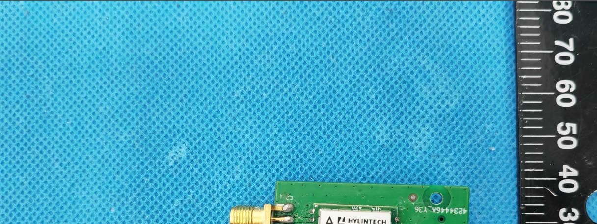
Click to zoom
Application Details
- Equipment Class
- DSS - Part 15 Spread Spectrum Transmitter
- Date of Grant
- Jun 28, 2023
- Application Purpose
- Original Equipment
- Date of Application
- Jun 28, 2023
- Equipment Note
- LoRa SPI Module
- Frequency Range
- 902.30000000 - 927.70000000
- Country
- China
Documents & Files
Document Text
Text extracted from the exhibit documents filed with the FCC. Open a document above to read the original.
Users Manual
HYLINTECH 杭 州 海 联 物 联 科 技有限公司 1 / 8 HYLINTECH HLM9S82 User Manual HYLINTECH 杭 州 海 联 物 联 科 技有限公司 2 / 8 HLM9S82 Datasheet 915M LoRa Module V1.3 Date:2022/12/01 Datasheet Discription HLM9S82 wireless module is a LoRa modulation based high performance IoT wireless transceiver. The module is developed based on SEMTECH's LLCC68 series RF integrated chip, which features small size, low power consumption, long transmission distance and strong anti-interference capability. HLM9S82 provides SPI interface, which is user-friendly and can be applied to various IoT wireless communication fields. Usage ⚫ Metering ⚫ Smart Home ⚫ Remote control ⚫ Security Features 902.3-927.7MHz LoRa Low power - 1.8V~3.6V Supply voltage - 5.3mA Rx mode - 1.2uA Sleep Mode ⚫ High link budget - Up to 22.10dBm Tx power - Rx sensitivity-129dBm@SF9BW125 ⚫ SPI Interface Order PN Range Size HLM9S82 -40°C~+85°C 18.6×18.5×3mm 18.6*18.5*3.0 mm FCC ID: 2A4G5-HLM9S82 HYLINTECH 杭 州 海 联 物 联 科 技有限公司 3 / 8 1 Specifications Table1-1 Absolute Maximum Ratings Table1-2 General Specifications Item Range Description Min Max VDD(V) -0.5 +3.8 Supply voltage Pmr(dBm) - +10 RF Input level Tmr(°C) -55 +125 Temperature Item Range Description Min Typ MAX VDD(V) 1.8 3.3 3.6 Supply voltage below 3.3V causes a drop in maximum transmit power. The module does not operate when the supply voltage is below 1.8V. Top(°C) -40 - 85 Operating temperature range Fa (kHz) -10 - +10 Frequency accuracy Fop (MHz) 902.3 - 927.7 Operating frequency band Power Consumption Tx (mA) 120 - Max power Tx Rx (mA) - 5.3 - DC_DC mode Sleep (uA) - 1.2 - SLEEP mode Tx Power (dBm) 22.10 Supply voltage = 3.3V Rx Sensitivity (dBm) - -129 - BW_L=125kHz , SF=9 Modem LoRa Size (mm) 18.6*18.6*3.0(Fig-2-1) GB/T1804-C - - HYLINTECH 杭 州 海 联 物 联 科 技有限公司 4 / 8 2 Package Outline Fig 2-1 HLM9S82 package outline HYLINTECH 杭 州 海 联 物 联 科 技有限公司 5 / 8 3 Pin Connection Table 3-1 Pin Description Pin Num Pin Name Type (I = input O = Output) Description P1 GND - Ground P2 RF I/O RF in and out P3 GND - Ground P4 SW_TX I Switch Control , Tx mode : High Level,Other mode : Low Level P5 SW_RX I Switch Control , Rx mode : High Level,Other mode : Low Level P6 DIO1 I/O LLCC68’s DIO1 P7 DIO2 I/O LLCC68’s DIO2 P8 DIO3 I/O LLCC68’s DIO3 P9 NRST I LLCC68’s NRESET P10 BUSY O LLCC68’s BUSY P11 NSS I LLCC68’s NSS P12 MISO O LLCC68’s MISO P13 SCLK I LLCC68’s SCLK P14 MOSI I LLCC68’s MOSI P15 VDD - Power supply P16 GND - Ground HYLINTECH 杭 州 海 联 物 联 科 技有限公司 6 / 8 4 Basic Operation 4.1 Typical application circuits When using the HLM9S82, users are advised to include a π-matching circuit between the module's antenna interface and the antenna interface, with the reference circuit structure shown in the diagram below. Fig4-1 is the optimum cost solution, requiring 11 IO ports; Fig4- 2 is the minimum IO ports solution, requiring 8 IO ports. Fig4-1 optimum cost solution Fig4-2 minimum IO ports solution Antenna Antenna HYLINTECH 杭 州 海 联 物 联 科 技有限公司 7 / 8 4.2 PCB Layout Notes 1. The DIO port is connected to the MCU's IO port with external interrupt. 2. The Trace between the RF port and the antenna is as short as possible. the RF Trac should be impedance matched (50Ω). 3. Add π-matching circuit between RF port and antenna if possible. 4. Keep the antenna away from other devices. 5. Keep away from high voltage circuits and high frequency circuits. 6. Ensure the quality of grounding, it is best to ensure a large area of paving. 4.3 SPI Interface The SPI interface gives access to the configuration register via a synchronous full-duplex protocol corresponding to CPOL = 0 and CPHA = 0 in Motorola/Freescale nomenclature. Only the slave side is implemented. An address byte followed by a data byte is sent for a write access whereas an address byte is sent and a read byte is received for the read access. The NSS pin goes low at the beginning of the frame and goes high after the data byte. MOSI is generated by the master on the falling edge of SCK and is sampled by the slave (i.e. this SPI interface) on the rising edge of SCK. MISO is generated by the slave on the falling edge of SCK. A transfer is always started by the NSS pin going low. MISO is high impedance when NSS is high. The SPI runs on the external SCK clock to allow high speed up to 16MHz. For detailed information, please refer to the LLCC68 chip instruction manual. Fig4-3 SPI Timing Diagram HYLINTECH 杭 州 海 联 物 联 科 技有限公司 8 / 8 5 Additional Notes 5.1Power Supply It is recommended to use a DC regulated power supply to power the HLM9S82 while keeping the power ripple as low as possible. HLM9S82 should be reliably grounded and the positive and negative terminals of the power supply should be properly connected, as reversing the connection may cause permanent damage to the module. 5.2 ESD The module can pass the electrostatic test of contact discharge 4KV and air discharge 8KV. During air discharge, the arc is approximately 10cm from the module. To avoid permanent damage to the device, all necessary ESD precautions should be taken. 5.4 Avoid using some frequencies Since the HLM9S82 uses a 32MHz crystal, crystal'frequency is 902.3-927.7MHz. Users should avoid these frequencies (>1MHz) when using the HLM9S82. FCC Statement Any Changes or modifications not expressly approved by the party responsible for compliance could void the user’s authority to operate the equipment. This devi ce complies with part 15 of the FCC Rules. Operation is subject to the following two conditions: (1)This device may not cause harmful interference, and (2)This device must accept any interference received, including interference that may cause undesired operation. Note: This equipment has been tested and found to comply with the limits for a Class B digital device, pursuant to part 15 of the FCC Rules. These limits are designed to provide reasonable protection against harmful interference in a residential installation. This equipment generates, uses and can radiate radio frequency energy and, if not inst …
Text truncated - open the document above for the full version.
Attestation Statements
Company: Hangzhou Hylin IoT Technology Co., Ltd. Add: No.80 Pingshui West Road,Xihu District,Hangzhou,China Te l : 13757198600 Fax: 13757198600 E-mail: [email protected] FCC Attestation Date: 2023-06-13 FEDERAL COMMUNICATIONS COMMISSION Authorization and Evaluation Division 7435 Oakland Mills Road Columbia, MD 21046 To whom it may concern: We, Hangzhou Hylin IoT Technology Co., Ltd., hereby authorize CHINA CERTIFICATION ICT CO., LTD (DONGGUAN) to act as a laboratory for testing and test report generation for the following project(s): (Product name: LoRa SPI Module, Model number: HLM9S82,FCC ID: 2A4G5-HLM9S82) The chip LLCC68 has activated LoRa functions and frequency range is 902.3-927.7MHz, Other functions are shielded by software and end user cannot activate it. This product only support FHSS , does’t support DTS. Please contact me if there is need for any additional clarification or information. Sincerely Yours, Signature: Printed Name: Sean Xu Title: CEO
Attestation Statements
Hangzhou Hylin IoT Technology Co., Ltd. CFR 47 §2.911(d)(5)(i)(ii) Attestation Letter Attestation Letter Date: 06/13/2023 FEDERAL COMMUNICATIONS COMMISSIONS Authorization and Evaluation Division 7435 Oakland Mills Road Columbia, MD 21046 Ref: Attestation Statements CFR 47 §2.911(d)(5)(i)(ii) Filing FCC ID: 2A4G5-HLM9S82 Hangzhou Hylin IoT Technology Co., Ltd. (“the applicant”) certifies that the equipment for which authorization is sought is not “covered” equipment prohibited from receiving an equipment authorization pursuant to section 2.903 of the FCC rules. Hangzhou Hylin IoT Technology Co., Ltd. (“the applicant”) certifies that as of the date of the filing of the application, the applicant is not identified on the Covered List as an entity producing “covered” equipment. Sincerely, Signature Contact Person: Sean Xu Title: CEO Company Name & Address: Hangzhou Hylin IoT Technology Co., Ltd. / No.80 Pingshui West Road,Xihu District,Hangzhou,China
Attestation Statements
U.S. AGENT LETTER OF ATTESTATION Date: 2023-06-13 FEDERAL COMMUNICATIONS COMMISSION Authorization and Evaluation Division 7435 Oakland Mills Road Columbia, MD 21046 Ref: Attestation Statements CFR 47 §2.911(d)(7) Filing FCC ID: 2A4G5-HLM9S82 Hangzhou Hylin IoT Technology Co., Ltd. (“the Applicant”) certifies that, as of the date of the filing of the application, Iconsigh Inc. is our designated U.S. agent for service of process for the above referenced FCC ID. Hangzhou Hylin IoT Technology Co., Ltd. (“the Applicant”) accepts to maintain an agent for no less than one year after the grantee has terminated all marketing and importation or the conclusion of any Commission-related proceeding involving the equipment. Iconsigh Inc. accepts, as of the date of the filing of the application, the obligation of the designated U.S. agent for service of process for the above referenced FCC ID. Designated U.S. Agent Information: Company Name: Iconsigh Inc. Address: 2310 Homestead Road, Suite C1, Los Altos, CA, 94024, USA FRN: 0033398652 Tel.: +1 (408) 320-9867 Email: [email protected] Signed by (printed name): Benjamin Kaur Signature: Applicant: Hangzhou Hylin IoT Technology Co., Ltd. Address: No.80 Pingshui West Road,Xihu District,Hangzhou,China FRN: 0031962707 Tel: 13757198600 Email: [email protected] Signed by (printed name): Sean Xu Signature:
Cover Letter(s)
Company name: Hangzhou Hylin IoT Technology Co., Ltd. Address: No.80 Pingshui West Road,Xihu District,Hangzhou,China Tel: 13757198600 Fax: 13757198600 Email: [email protected] FCC Authorization Date:2023-06-13 FEDERAL COMMUNICATIONS COMMISSION Authorization and Evaluation Division 7435 Oakland Mills Road Columbia, MD 21046 Subject: Agent Authorization To whom it may concern: We, Hangzhou Hylin IoT Technology Co., Ltd. Hereby authorizes CHINA CERTIFICATION ICT CO., LTD (DONGGUAN) to act on its behalf in all matters relating to application for Equipment authorization, including the signing of all documents relating to these matters. All acts carried out by CHINA CERTIFICATION ICT CO., LTD (DONGGUAN) on our behalf shall have the same effect as our own action. We, the undersigned, hereby certify that we are not subject to a denial of federal benefits, that includes FCC benefits, pursuant to Section 5301 of the Anti-Drug Abuse Act of 1988, 21 U.S.C. 862. This authorization is valid until further written notice from the applicant. Sincerely Yours, Signature: Printed Name: Sean Xu Title: CEO QA-FR-170-B
Cover Letter(s)
QA-FR-171-A Company name: Hangzhou Hylin IoT Technology Co., Ltd. Address: No.80 Pingshui West Road,Xihu District,Hangzhou,China Tel: 13757198600 Fax: 13757198600 Email: [email protected] FCC Confidential Authorization Date: 2023-06-13 FEDERAL COMMUNICATIONS COMMISSIONS Authorization and Evaluation Division 7435 Oakland Mills Road Columbia, MD 21046 Subject: Confidentiality Request regarding application for certification of FCC ID: 2A4G5-HLM9S82 In accordance with Sections 0.457 and 0.459 of the Commission’s Rules, Hangzhou Hylin IoT Technology Co., Ltd. hereby requests long-term confidential treatment of information accompanying this application as outlined below: • Block Diagram • Schematics • Operation Description The above materials contain proprietary and confidential information not customarily released to the public. The public disclosure of these materials provides unjustified benefits to its competitors in the market. Sincerely, Signature: Printed Name: Sean Xu Title: CEO
Cover Letter(s)
Company Name: Hangzhou Hylin IoT Technology Co., Ltd. Add: No.80 Pingshui West Road,Xihu District,Hangzhou,China Tel: 13757198600 Fax: 13757198600 E- mail: [email protected] Modular Approval Letter Date:2023-06-13 FEDERAL COMMUNICATIONS COMMISSIONS Authorization and Evaluation Division 7435 Oakland Mills Road Columbia, MD 21046 We, Hangzhou Hylin IoT Technology Co., Ltd., hereby request Modular Approval for Product: LoRa SPI Module (Model number: HLM9S82), FCC ID: 2A4G5- HLM9S82).The EUT meets all of the requirement for modular approval as detailed in FCC 15.212. the requirements is described below: 1.The modular has RF shielding, please refer to the EUT photo. 2.The modular transmitter has buffered modulation/data inputs, Buffered data inputs stage has been integrated in chip (Model: LLC C68). 3.The modular transmitter has its own power supply regulation. Please refer to the schematic. 4.Comply with the antenna requirements of Section 15.203 and 15.204(c), the modular test with a dipole an tenna which use a unique type of connector to attached to the module, the maximum gain is 1.03dBi. 5.The EUT was tested in a stand-alone configuration, please refer to setup photos exhibit for details. 6.The module labeled with its own FCC ID. 7.Comply with any specific rules or operating requirements that ordinarily apply to a complete transmitter and the manufacturer must provide adequate instructions along with the module to explain any such requirements. The necessary explanation to be complied with this requirement is contained in the user manual, band please refers to the User Manual. 8.Comply with FCC §15.247 (i) & §1.1307(b)(3)(i)(C) RF exposure requirements in its final configuration. Sincerely, Si gnature: Printed Name: Sean Xu Title: CEO
External Photos
EXHIBIT B - EUT EXTERNAL PHOTOGRAPHS Test Board EUT EUT Antenna Port Antenna Port Antenna
ID Label/Location Info
A � HYLINTECH Mo de l: HLM9S82 FCC ID:.ZA芯S..l-tLM9Sll2 喝 回向 DOC 00? lOF008 .. 3 0 0 200 8ll N I S4 0 0
Internal Photos
EXHIBIT C - EUT INTERNAL PHOTOGRAPHS
RF Exposure Info
China Certification ICT Co., Ltd (Dongguan) Report No.: CR230205016-00 Page 47 of 47 5. RF EXPOSURE EVALUATION 5.1 Applicable Standard FCC §15.247 (i) and subpart §1.1307 Systems operating under the provisions of this section shall be operated in a manner that ensures that the public is not exposed to radio frequency energy level in excess of the Commission’s guidelines. 5. 2 Procedure According to §1.1307(b)(3)(i) (C) Or using Table 1 and the minimum separation distance (R in meters) from the body of a nearby person for the frequency (f in MHz) at which the source operates, the ERP (watts) is no more than the calculated value prescribed for that frequency. For the exemption in Table 1 to apply, R must be at least λ/2π , where λ is the free-space operating wavelength in meters. If the ERP of a single RF source is not easily obtain ed, then th e available maximum time-averaged power may be used in lieu of ERP if the physical dimensio ns o f the radiating structure(s) do not exceed the electrical length of λ/4 or if the antenna gain is less than that of a half-wave dipole (1.64 linear value). Table 1 to § 1.1307(b)(3)(i)(C) - Single RF Sources Sub ject to Routine Environmental Evaluation RF Source frequency (MHz) Threshold ERP (watts) 0.3-1.341,920 R 2 . 1.34-303,450 R 2 /f 2 . 30-3003.83 R 2 . 300-1,5000.0128 R 2 f. 1,500-100,00019.2R 2 . 5 .3 Measurement Result Operation Modes Frequency (MHz) λ/2π (mm) Distance (mm) Exemption ERP (mW) Maximum Conducted Power including Tune- up Tolerance (dBm) Antenna Gain (dBi) ERP MPE- Based Exemption (dBm) (mW) Lora-FHSS 902.3- 927.7 52.94 200 462 23 1 .03 21.88 154.17 Compliant Note: The Maximum Conducted Power including Tune-up Tolerance was declared by manufacturer. Result: The device compliant the MPE-Based Exemption at 20cm distances. ===== END OF REPORT =====
Test Report
产 品 承 认 书 (SPECIFICATION) 日期/DATE: 2023 /01/10 编号/NUMBER:205940-1 版本/VERSION:A1 晟天编号: PART MODEL:HZ5940N-1.5M 产品名称: PRODUCTNAME :915MHz ANT 1.5M-RPSMA-J Manufacturer:Sunsky Technology Co.,Ltd 8/F, No.614 Building, Bagua 1st Road, Futian District 1、产品技术指标(PRODUCT TECHNICAL SPECIFICATION) 电性能指标Electrical Specifications 频率范围Frequency Range (MHz) 824-960 频带宽度Bandwidth (MHz) 140 输入阻抗Input Impendence (Ω) 50 电压驻波比V.S.W.R ≤ 2 增益Gain 1.03dBi @900~928MHz 极化形式Polarization Type Vertical 功率容量Power Capacity (w) 50 机械指标Mechanical Specifications 线缆长度 Antenna Length (mm) 1500 mm 连接器型号Connect Type RPSMA-J (Customize) 外壳颜色Radome Color 黑色 Black 重量Weight (g) (15)g (Without cable) 2、产品图片(Product picture) 5、测试图片(Test picture)
Test Report
TEST REPORT Applicant: Hangzhou Hylin IoT Technology Co.,Ltd. Ad dress: No.80 Pingshui West Road, xihu District, Hangzhou, China FCC ID: 2A4G5-HLM9S82 Product Name: LoRa SPI Module Standard(s): 47 CFR Part 15, Subpart C(15.247) ANSI C63.10-2013 KDB 558074 D01 15.247 Meas Guidance v05r02 The above equipment has been tested and found compliant with the requirement of the relative standards by China Certification ICT Co., Ltd (Dongguan) Report Number: CR230205016-00 Date Of Issue: 2023/06/28 Reviewed By: Sun Zhong Title: Manager Test Laboratory: China Certification ICT Co., Ltd (Dongguan) No. 113, Pingkang Road, Dalang Town, Dongguan, Guangdong, China Tel: +86-769-82016888 China Certification ICT Co., Ltd (Dongguan) Report No.: CR230205016-00 Page 2 of 47 Test Facility The Test site used by China Certification ICT Co., Ltd (Dongguan) to collect test data is located on the No. 113, Pingkang Road, Dalang Town, Dongguan, Guangdong, China. The lab has been recognized as the FCC accredited lab under the KDB 974614 D01 and is listed in the FCC Public Access Link (PAL) database, FCC Registration No. : 442868, the FCC Designation No. : CN1314. The lab has been recognized by Innovation, Science and Economic Development Canada to test to Canadian radio equipment requirements, the CAB identifier: CN0123. Declarations China Certification ICT Co., Ltd (Dongguan) is not responsible for the authenticity of any test data provided by the applicant. Data included from the applicant that may affect test results are marked with a triangle symbol “▲”. Customer model name, addresses, names, trademarks etc. are not considered data. Unless otherwise stated the results shown in this test report refer only to the sample(s) tested. This report cannot be reproduced except in full, without prior written approval of the Company. This report is valid only with a valid digital signature. The digital signature may be available only under the Adobe software above version 7.0. This report may contain data that are not covered by the accreditation scope and shall be marked with an asterisk “★”. China Certification ICT Co., Ltd (Dongguan) Report No.: CR230205016-00 Page 3 of 47 CONTENTS T EST FACILITY .......................................................................................................................................... 2 DECLARATIONS .......................................................................................................................................... 2 DOCUMENT REVISION HISTORY .......................................................................................... 5 1. GENERAL INFORMATION .................................................................................................... 6 1.1 PRODUCT DESCRIPTION FOR EQUIPMENT UNDER TEST (EUT) ....................................................... 6 1.2 DESCRIPTION OF TEST CONFIGURATION ........................................................................................... 8 1.2.1 EUT Operation Condition: ............................................................................................................................. 8 1.2.2 Support Equipment List and Details .............................................................................................................. 8 1.2.3 Support Cable List and Details ...................................................................................................................... 8 1.2.4 Block Diagram of Test Setup ......................................................................................................................... 9 1.3 MEASUREMENT UNCERTAINTY ........................................................................................................ 10 2. SUMMARY OF TEST RESULTS .......................................................................................... 11 3. REQUIREMENTS AND TEST PROCEDURES .................................................................. 12 3.1 AC LINE CONDUCTED EMISSIONS .................................................................................................... 12 3.1.1 Applicable Standard ..................................................................................................................................... 12 3.1.2 EUT Setup.................................................................................................................................................... 13 3.1.3 EMI Test Receiver Setup ............................................................................................................................. 13 3.1.4 Test Procedure ............................................................................................................................................. 14 3.1.5 Corrected Amplitude & Margin Calculation ................................................................................................ 14 3.2 RADIATION SPURIOUS EMISSIONS .................................................................................................... 15 3.2.1 Applicable Standard ..................................................................................................................................... 15 3.2.2 EUT Setup.................................................................................................................................................... 15 3.2.3 EMI Test Receiver & Spectrum Analyzer Setup ......................................................................................... 16 3.2.4 Test Procedure ............................................................................................................................................. 16 3.2.5 Corrected Amplitude & Margin Calculation ................................................................................................ 16 3.3 20 DB BANDWIDTH ............................................................................................................................. 1 7 3.3.1 Appli…
Text truncated - open the document above for the full version.
Test Setup Photos
EXHIBIT D - TEST SETUP PHOTOGRAPHS Conducted Emissions Front View Conducted Emissions Side View Radiated Emission Below 1GHz View Radiated Emission Above 1GHz View
Contact Information
Applicant
Sean Xu(CEO)
Test Firm
CHINA CERTIFICATION ICT CO., LTD (DONGGUAN)Tanie Ou
[email protected]0086 0769 86858888
Technical Specifications
| # | Rule Parts | Frequency Range | Power Output |
|---|---|---|---|
| 1 | 15C | 902.3 MHz - 927.7 MHz | 160.00 mW |
Other Applications from Hangzhou Hylin IoT Technology Co., Ltd.

2A4G5-HLM9521
Dec 02, 2023HLM9521-HW4
Equipment Class
DTS - Digital Transmission System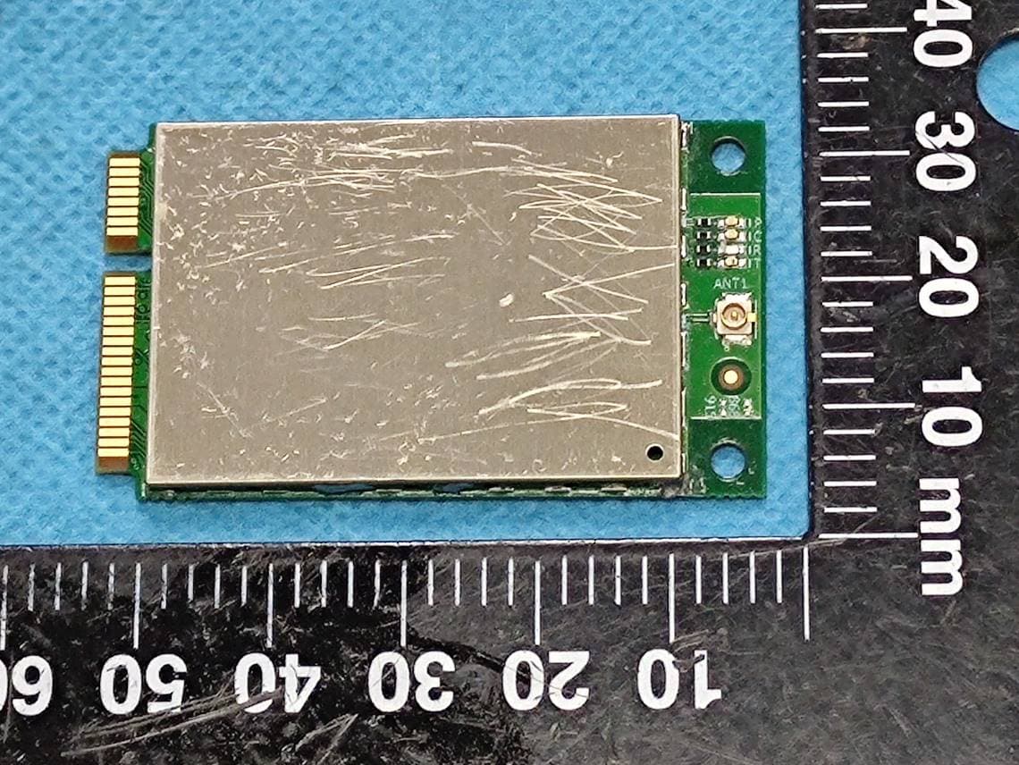
2A4G5-HLM9933
Jul 17, 2022SX1302 Gateway Module
Equipment Class
DSS - Part 15 Spread Spectrum Transmitter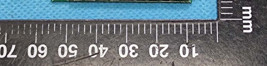
2A4G5-HLM5934
Jul 14, 2022SX1302 Gateway Module
Equipment Class
DTS - Digital Transmission System