2A8SQ-M8wireless lavalier microphone
ShenZhen ZhiWei Technology Co., Ltd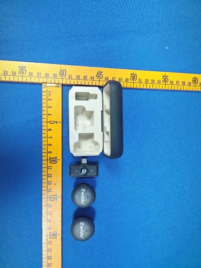
Click to zoom
Application Details
- Equipment Class
- DTS - Digital Transmission System
- Date of Grant
- Apr 16, 2024
- Application Purpose
- Original Equipment
- Date of Application
- Apr 16, 2024
- Equipment Note
- wireless lavalier microphone
- Frequency Range
- 2402.00000000 - 2480.00000000
- Country
- China
Documents & Files
Document Text
Text extracted from the exhibit documents filed with the FCC. Open a document above to read the original.
External Photos
FCCID:2A8SQ-M8 FCCID:2A8SQ-M8 FCCID:2A8SQ-M8 FCCID:2A8SQ-M8
Internal Photos
FCCID:2A8SQ-M8 FCCID:2A8SQ-M8 FCCID:2A8SQ-M8 FCCID:2A8SQ-M8 ANT FCCID:2A8SQ-M8
RF Exposure Info
Page1of2 RFEXPOSUREEVALUATION FCCID:2A8SQ-M8 ProductName:wirelesslavaliermicrophone ModelName:M8 Additionalmodelname:M7,C8 BluetoothVersion:BTBDRandBLE Operatingfrequency:2402-2480MHz NumbersofChannel: 40channelsForDTS 79channelsforBDR AntennaType:CeramicAntenna AntennaGain:2.71dBi TypeofModulation:GFSK Powersupply: Input:DC5.0V1.0A Li-ionBattery:752630 RatedVoltage:3.7V RatedCapacity:600mAh HardwareVersion:XY-Q8-TX-V3 SoftwareVersion:N/A Page2of2 StandardRequirement Accordingto§15.247(i)and§1.1307b(1),systemsoperatingundertheprovisionsofthis sectionshallbeoperatedinamannerthatensuresthatthepublicisnotexposedtoradio frequencyenergylevelsinexcessoftheCommission’sguidelines.SeeKDB447498D01 GeneralRFExposureGuidancev06,section4.3.1. The1-gand10-gSARtestexclusionthresholdsfor100MHzto6GHzattestseparation distances≤50mmaredeterminedby: [(max.powerofchannel,includingtune-uptolerance,mW)/(min.testseparationdistance, mm)]*[√f(GHz)]≤3.0for1-gSARand≤7.5for10-gSARextremitySAR,where f(GHz)istheRFchanneltransmitfrequencyinGHz PoweranddistanceareroundedtothenearestmWandmmbeforecalculation Theresultisroundedtoonedecimalplaceforcomparison. Thetestexclusionsareapplicableonlywhentheminimumtestseparationdistanceis≤ 50mmandfortransmissionfrequenciesbetween100MHzand6GHz.Whentheminimumtest separationdistanceis<5mm,adistanceof5mmisappliedtodetermineSARtestexclusion. RoutineSARevaluationreferstothatspecificallyrequiredby§2.1093,usingmeasurements orcomputersimulation.WhenroutineSARevaluationisnotrequired,portabletransmitters withoutputpowergreaterthantheapplicablelowthresholdrequireSARevaluationtoquality forTCBapproval. Channel (MHz) Maximum output power (dBm) Tuneup tolerance (dBm) MaxTune UpPower (mW) Distance (mm) Calculation results Limit Operating Mode 2480 5.31 5.31 ± 14.27562951.3466533EDR(3DH5) 24802.002.00±11.99526250.6284283BLE AccordingtoKDB447498,nostand-alonerequiredforBTantenna,andnosimultaneousSAR measurementisrequired. Signature SimonPu Manager Date:2024-04-15
Test Report
A3216H2G50M200- Guangdong Dongyou Technology Co., Ltd 03 Room 202, Building 10, No.1 Jingdong Road, Fenggang Town, Dongguan City, Guangdong Province A3216H2G50M200-03 chip antenna ※ Product Features: ⚫ The whole is surface mounting device It has the characteristics of small volume, low shape and light weight ⚫ Wide frequency band ⚫ Be certified lead-free ⚫ The dimensions are :3.2x1.6x0.4mm ※ Application: ⚫ Bluetooth/WLAN/home RF technology ⚫ ISM band 2.4GHz applications A3216H2G50M200- Guangdong Dongyou Technology Co., Ltd 03 Technical indicators: Part number information: A 3216 H 2G50 M200 - 03 A Antenna 2G50 The center frequency is 2.5G 3216 Dimensions 3.2x1.6 M200 Band width 200M H electrosensibility 03 Product model number Center frequency 2.50 GHz Band width 100MHz(typ.) Maximum gain 2.71dBi(typ.) (XZ-V) Average gain 0.5dBi(typ.) (XZ-V) Voltage standing wave ratio < 2 Impedance 50 Ω Power capacity 3 W(max) Operating temperature -40 ~ +85 °C Storage temperature -40 ~ +85 °C A3216H2G50M200-03 Room 202, Building 10, No.1 Jingdong Road, Fenggang Town, Dongguan City, Guangdong Province 2 1 Pin Guangdong Dongyou Technology Co., Ltd Description of structure: No. 1 2 Pin allocation Feed end Fixed end Note: One of these two pads is connected to the RF signal and the other is used to hold without receiving any signal. The left and right sides of these two pads are perfectly symmetrical and do not distinguish between positive and negative and left and right. Size description: A1 | | W H L Units (mm) L W H A1 Overall dimensions 3.2 + / - 0.05 1.6 ± 0.05 0.4 ± 0.05 0.35 ± 0.05 A3216H2G50M200- Guangdong Dongyou Technology Co., Ltd 03 Room 202, Building 10, No.1 Jingdong Road, Fenggang Town, Dongguan City, Guangdong Province Antenna placement and clearance processing and matching network diagram Matching device values Parallel device Shunt 1 1.7 nH Series Device Series 1 2.4 nH Shunt device 2 NC Impedance matching is required for any type of antenna to ensure that the antenna performance meets the requirements of the impedance specification, The A3216H2G50M200-03 patch antenna also needs to add a matching network to ensure the antenna performance meets the standards. Three matching devices together form π-type matching network for the impedance matching of A3216H2G50M200-03 patch antenna. The specific device values of these matching devices need to be obtained after antenna impedance matching and debugging. The device values shown above are the values of our test circuit board and can be used as reference values. If you do not have high requirements for antenna performance, you can also directly use the above reference values. The line width should match the 50 ohm characteristic impedance according to the PCB material and thickness design. It is recommended to place the antenna on the edge or corner of the board, do not place the antenna in the middle of the board and do not allow the antenna to be surrounded by conductors. Gaps are needed near the antenna area of the board. As shown above, the blank area on the board (the white area) is the gap area of the antenna. The so-called A3216H2G50M200- Guangdong Dongyou Technology Co., Ltd 03 clearance area refers to the area that cannot be paved and wired except for the antenna pad and antenna signal wiring. The clearance treatment of this area should be for all layers of the PCB board, not just the surface layer. The headroom area of the antenna should be as large as possible, and the antenna should be placed as close as possible to the edge of the board, so that the antenna body is far away from the board, and the larger the headroom means the better the antenna efficiency and gain performance. In the structure of the whole machine, it is recommended that there should be no conductor in the overhead area above or below the direction of overlooking the PCB, otherwise the antenna performance will be affected. The non-clearance area needs to be paved, and the ground should be increased as much as possible through the hole connection between the layers. A3216H2G50M200- Guangdong Dongyou Technology Co., Ltd 03 The equipment used for antenna matching debugging is the network analyzer. If you are an antenna professional technician, you can perform antenna matching debugging with the network analyzer that comes with you. If you do not have the relevant technology, please contact us and we can provide it for your product Professional antenna impedance debugging services. Antenna matching debugging needs to provide the entire product (no need to open it). Note that antenna impedance matching debugging mentioned here has nothing to do with RF line impedance control. Rf line impedance control is only for RF line wiring in paved areas, where the matched antenna impedance is the antenna. Please do not confuse the two. 2. The performance parameters of antenna matching after debugging are shown in the figure below: S11 Log Mag: A3216H2G50M200-03 Guangdong Dongyou Technology Co.,Ltd S11 Smith R+jx: A3216H2G50M200- Guangdong Dongyou Technology Co., Ltd 03 S11SWR: A3216H2G50M200- Guangdong Dongyou Technology Co., Ltd 03 Efficiency Peak Gain Directivity 2400MHz 55.21% 1.45 dBi 5.32 dBi 2450MHz 66.45% 2.71 dBi 5.21 dBi 2500MHz 57.53% 1.98 dBi 5.29 dBi A3216H2G50M200- Guangdong Dongyou Technology Co., Ltd 03 3, reliability and test conditions Items requirement TEST CONDITION Weldability test 1. Wettability should exceed 90% coverage 2. No visible mechanical damage temperature Heating temperature :150 c / 60 seconds. Welding temperature :230±5 c Duration :4±1 SEC. Welding :Sn- Ag3.0-Cu0.5 Lead-free flux: rosin 230 °C 150C 4±1 sec. 60sec Heat resistance of solder 1. No obvious mechanical damage 2. Center frequency change :±6% or less TEMP ( C) 260°C 10±0.5 sec. 150 C 60sec Heating temperature :150 c / 60 SEC. Welding temperature :260±5 c Duration :10±0.5 seconds. Welding :Sn-Ag3.0- Cu0.5 Lead-free flux: rosin Component adhesion (Push-push test) 1. No obvious mechanical dama…
Text truncated - open the document above for the full version.
Test Report
Page1 of 56 FCC TEST REPORT FCC ID: 2A8SQ -M8 Product: wirelesslavaliermicrophone ModelName: M8, M7,C8 Brand: N/A ReportNo.: PTC24032608801E-FC02 Preparedfor ShenZhenZhiWeiTechnologyCo., Ltd East of 3F Bld 3,LiJinChengIndustrialPark, YousongComm,LonghuaStr, LonghuaDis, Shenzhen,China Preparedby PreciseTesting& CertificationCo., Ltd Building1, No. 6, TongxinRoad,DongchengStreet,Dongguan,Guangdong,China ReportNo.: PTC24032608801E-FC02 Page2 of 56 1 TEST RESULT CERTIFICATION Applicant’s name:ShenZhenZhiWeiTechnologyCo., Ltd Address: East of 3F Bld 3,LiJinChengIndustrialPark, YousongComm,Longhua Str, LonghuaDis, Shenzhen,China Manufacture'sname:ShenZhenZhiWeiTechnologyCo., Ltd Address: East of 3F Bld 3,LiJinChengIndustrialPark, YousongComm,Longhua Str, LonghuaDis, Shenzhen,China Productname:wirelesslavaliermicrophone Modelname:M8, M7,C8 Standards:FCC CFR47Part 15 Section15.247 Test procedure:ANSIC63.10:2013 Test Date: Mar. 28, 2024to Apr. 12, 2024 Dateof Issue: Apr. 15, 2024 Test Result:Pass This devicedescribedabovehas beentestedby PTC,and the test resultsshowthat the equipmentundertest (EUT)is in compliancewith the FCC requirements.And it is applicableonly to the testedsampleidentifiedin the report. This reportshall not be reproducedexceptin full, withoutthe writtenapprovalof PTC,this document may be alteredor revisedby PTC,personalonly,and shall be notedin the revisionof the document. Test Engineer: Jackzhou/ Engineer TechnicalManager: SimonPu / Manager ReportNo.: PTC24032608801E-FC02 Page3 of 56 Contents Page 1 TEST RESULT CERTIFICATION...............................................................................................................................2 2 TEST SUMMARY..........................................................................................................................................................5 2.1 TESTSITE............................................................................................................................................................6 3 GENERALINFORMATION.......................................................................................................................................7 3.1 GENERALDESCRIPTIONOFE.U.T.....................................................................................................................7 3.2 CHANNELLIST.....................................................................................................................................................8 4 EQUIPMENTDURINGTEST....................................................................................................................................9 4.1 EQUIPMENTSLIST.............................................................................................................................................9 4.2 MEASUREMENTUNCERTAINTY.........................................................................................................................11 4.3 DESCRIPTIONOFSUPPORTUNITS...................................................................................................................12 5 CONDUCTEDEMISSION..........................................................................................................................................13 5.1 E.U.T.OPERATION............................................................................................................................................13 5.2 EUT SETUP.......................................................................................................................................................13 5.3 TESTSET-UP(BLOCKDIAGRAMOFCONFIGURATION).................................................................................14 5.4 MEASUREMENTPROCEDURE............................................................................................................................14 5.5 CONDUCTEDEMISSIONLIMIT...........................................................................................................................14 5.6 MEASUREMENTDESCRIPTION..........................................................................................................................14 5.7 CONDUCTEDEMISSIONTESTRESULT.............................................................................................................14 6 RADIATEDSPURIOUSEMISSIONS......................................................................................................................17 6.1 EUT OPERATION...............................................................................................................................................17 6.2 TESTSETUP......................................................................................................................................................18 6.3 SPECTRUMANALYZERSETUP..........................................................................................................................19 6.4 TESTPROCEDURE.............................................................................................................................................20 6.5 SUMMARYOFTESTRESULTS...........................................................................................................................22 7 CONDUCTBANDEDGEAND SPURIOUSEMISSIONSMEASUREMENT....................................................29 7.1 TESTPROCEDURE.............................................................................................................................................29 7.2 TESTSETUP......................................................................................................................................................29 7.3 TESTRESULT....................................................................................................................................................30 ReportNo.: PTC24032608801E-FC02 Page4 of 56 8 6DB BANDWIDTHMEASUREMENT....................................................................…
Text truncated - open the document above for the full version.
Test Setup Photos
FCCID:2A8SQ-M8 ConductedEmissions RadiatedSpuriousEmissions From30MHz-1000MHz FCCID:2A8SQ-M8 TestfrequencyfromAbove1GHz
Contact Information
Applicant
Qiang Zhou(General Manager)
Test Firm
Precise Testing & Certification Co., LTD.Chris Du
[email protected]+86-769-38808222
Technical Specifications
| # | Rule Parts | Frequency Range | Power Output |
|---|---|---|---|
| 1 | 15C | 2.40 GHz - 2.48 GHz | 1.60 mW |
Other Applications from ShenZhen ZhiWei Technology Co., Ltd
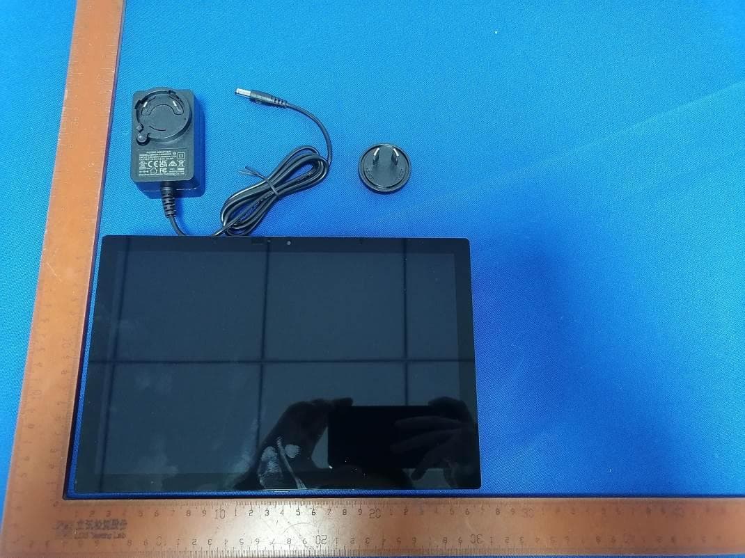
2A8SQ-IST-10
Aug 07, 2024Tablet computer
Equipment Class
DSS - Part 15 Spread Spectrum Transmitter
2A8SQ-IST-5
Aug 01, 2024Tablet computer
Equipment Class
DTS - Digital Transmission System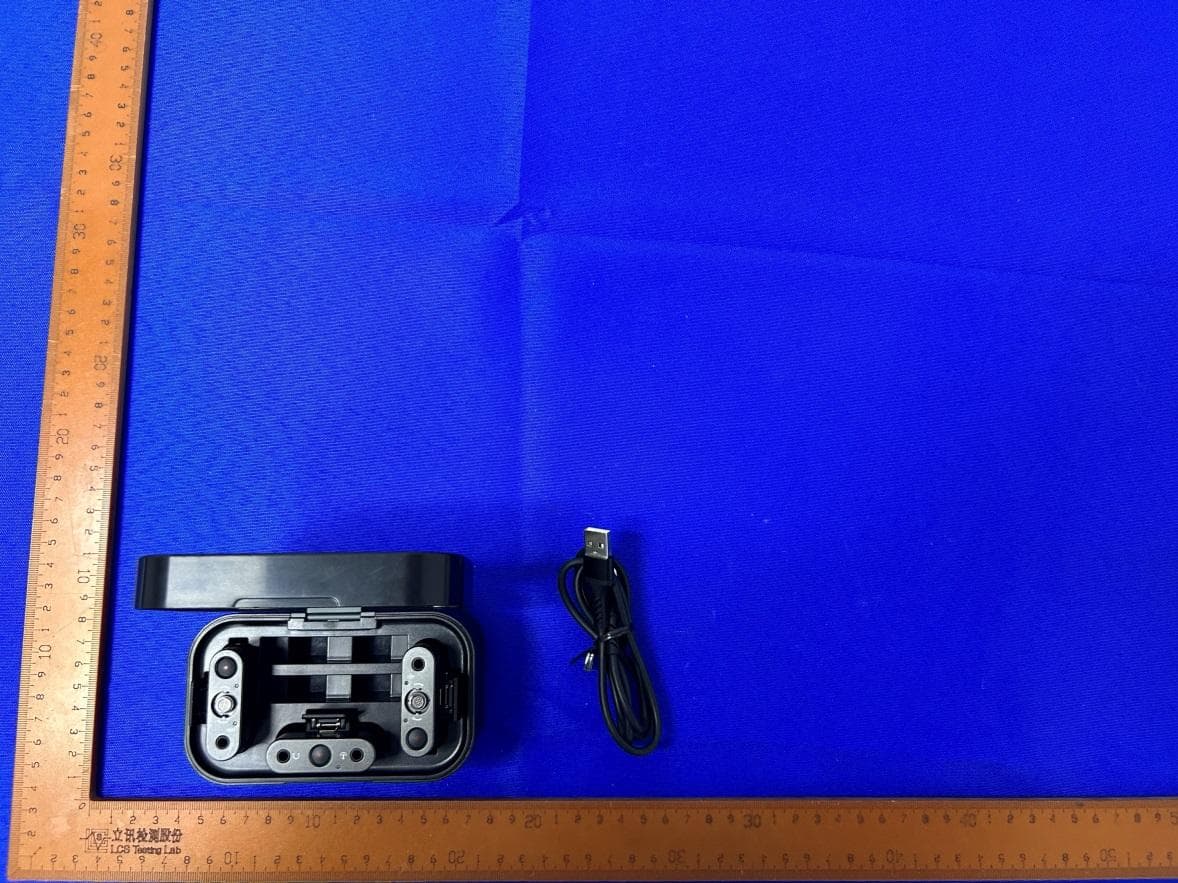
2A8SQ-C2
May 04, 2023Wireless Lavalier Microphone
Equipment Class
DTS - Digital Transmission System