2AANZWECCWireless Earbuds
DGL Group LTD.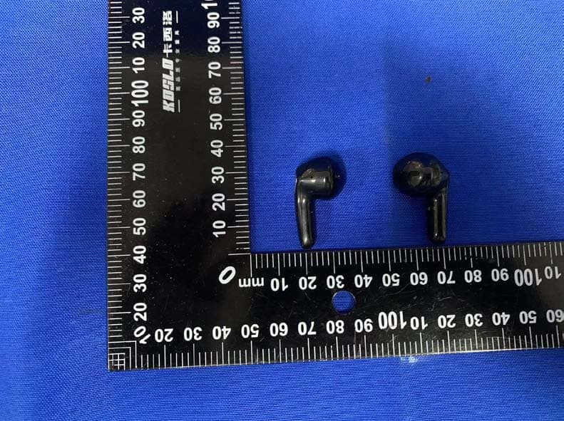
Click to zoom
Application Details
- Equipment Class
- DSS - Part 15 Spread Spectrum Transmitter
- Date of Grant
- Nov 09, 2022
- Application Purpose
- Original Equipment
- Date of Application
- Nov 09, 2022
- Equipment Note
- Wireless Earbuds
- Frequency Range
- 2402.00000000 - 2480.00000000
- Company
- DGL Group LTD.
- Country
- United States
Documents & Files
Document Text
Text extracted from the exhibit documents filed with the FCC. Open a document above to read the original.
Attestation Statements
DGL Group LTD. 2045 Lincoln Highway, 3rd floor, Edison, New Jersey, United States ,08817 Tel: 001-732-692-5180 Fax: 001-732-692-5000 E- Mail: [email protected] Date:10/12/2022 To : FEDERAL COMMUNICATIONS COMMISSION Authorization and Evaluation Division 7435 Oakland Mills Road Columbia, MD 21046 We, DGL Group LTD. hereby declare that: Product Name: Wireless Earbuds Model No.: FB-WECC-MC1 FCC ID: 2AANZWECC For BT Mode: BLE 1M/2M are disable by software For Below are activated: Bluetooth BDR(GFSK) ,EDR(π/4‐DQPSK ,8DPSK) Except for the manufacturer, the end user does not have any capability to modify/change the RF parameters. We acknowledge that it is the manufacturer’s responsibility to provide the radio configurations to ensure compliance with Commission’s rules. . Sincerely Yo u rs, Signature: Printed Name: Amy Chao Title: Manager
Attestation Statements
DGL Group LTD. 2045 Lincoln Highway, 3rd floor, Edison, New Jersey, United States ,08817 Tel: 001-732-692-5180 Fax: 001-732-692-5000 E- Mail: [email protected] Date:1 0/12/ 2022 We, DGL Group LTD., h ereby declare that Our product, Wireless Earbuds, Model number: FB-WECC-MC1, FCC ID: 2AANZWECC is a twin earphone that has a left earphone and a right earphone. We would like to declare that the left earphone and the right earphone are identical in the Antenna & RF circuits. So only choose the one of two earphones to test. We confirm that all information above is true, and we’ll be responsible for all the consequences. Please contact me if you have any question. Sincerely Yours, Signature: Printed Name: Amy Chao Title: Manager Type text here
Block Diagram
5616A SPK 26M M I C Touch Battery protection 5V Crystal ANT 2402-2480MHz
Cover Letter(s)
DGL Group LTD. 2045 Lincoln Highway, 3rd floor, Edison, New Jersey, United States ,08817 Tel: 001-732-692-5180 Fax: 001-732-692-5000 E- Mail: [email protected] FCC Authorization 10/12/2022 FEDERAL COMMUNICATIONS COMMISSIONS Authorization and Evaluation Division 7435 Oakland Mills Road Columbia, MD 21046 Subject: Agent Authorization To whom it may concern: We, DGL Group LTD., the undersigned, hereby authorize Shenzhen Accurate Technology Co., Ltd to act on its behalf in all matters relating to application for Equipment authorization, including the signing of all documents relating to these matters. All acts carried out by Shenzhen Accurate Technology Co., Ltd on our behalf shall have the same effect as our own action. We, the undersigned, hereby certify that we are not subject to a denial of federal benefits, that includes FCC benefits, pursuant to Section 5301 of the Anti-Drug Abuse Act of 1988, 21 U.S.C. 862. This authorization is valid until further written notice from the applicant. Sincerely Yours, Signature: Printed Name: Amy Chao Title: Manager
Cover Letter(s)
DGL Group LTD. 2045 Lincoln Highway, 3rd floor, Edison, New Jersey, United States ,08817 Tel: 001-732-692-5180 Fax: 001-732-692-5000 E- Mail: [email protected] Date:10/12/2022 FCC ID Cover Letter The DGL Group LTD. here by submits justification for placing the FCC ID in the Associated User Manual. According to the FCC Regulation and Guidance (KDB Publication 784748 D01 v09r01) allows for the FCC ID to be moved to the User’s manual if the device is unquestionably too small for the FCC ID to be printed. Referring to the above quote, as the device is too small (FCC ID: 2AANZWECC ) to be printed. The FCC ID will be moved to the last page of user’s manual and charging case. The details are as below: A. Side surface (A): The curvature shape of the silicone sleeve back cover is not flat, so it’s hard to affix thelabel on the surface of the earbuds. B. Top cover (B): The plastic logo of the top cover does not provide enough physical space to fit the printing of the FCC ID according to below reference picture. Conclusion: Based on the above description of area A to B, we conclude that the device is unquestionably too samll for enabling the FCC ID to be printed onto any surface, We therefore request to move the FCC ID to the User manual and charging case Sincerely Yours, Signature: Printed Name: Amy Chao Title: Manager
External Photos
Shenzhen Accurate Technology Co., Ltd. Project No.: SZ3220928-44491E-RF Page 1 of 6 External Photos Shenzhen Accurate Technology Co., Ltd. Project No.: SZ3220928-44491E-RF Page 2 of 6 Shenzhen Accurate Technology Co., Ltd. Project No.: SZ3220928-44491E-RF Page 3 of 6 Shenzhen Accurate Technology Co., Ltd. Project No.: SZ3220928-44491E-RF Page 4 of 6 Shenzhen Accurate Technology Co., Ltd. Project No.: SZ3220928-44491E-RF Page 5 of 6 Shenzhen Accurate Technology Co., Ltd. Project No.: SZ3220928-44491E-RF Page 6 of 6
ID Label/Location Info
Shenzhen Accurate Technology Co., Ltd. Project No.: SZ3220928-44491E-RF LABEL AND LOCATION Page 1 of 1 FCC ID Label FCC ID Label Location Information The label shown shall be permanently affixed at a conspicuous location on the device and be readily visible to the user at the time purchase (Labeling requirements per 2.925)
Internal Photos
Shenzhen Accurate Technology Co., Ltd. Project No.: SZ3220928-44491E-RF Page 1 of 9 Internal photos Right earbud uncover Left earbud uncover Shenzhen Accurate Technology Co., Ltd. Project No.: SZ3220928-44491E-RF Page 2 of 9 Shenzhen Accurate Technology Co., Ltd. Project No.: SZ3220928-44491E-RF Page 3 of 9 Shenzhen Accurate Technology Co., Ltd. Project No.: SZ3220928-44491E-RF Page 4 of 9 Antenna Shenzhen Accurate Technology Co., Ltd. Project No.: SZ3220928-44491E-RF Page 5 of 9 Shenzhen Accurate Technology Co., Ltd. Project No.: SZ3220928-44491E-RF Page 6 of 9 Shenzhen Accurate Technology Co., Ltd. Project No.: SZ3220928-44491E-RF Page 7 of 9 Shenzhen Accurate Technology Co., Ltd. Project No.: SZ3220928-44491E-RF Page 8 of 9 Shenzhen Accurate Technology Co., Ltd. Project No.: SZ3220928-44491E-RF Page 9 of 9
Operational Description
Circuit Description Battery (DC 3.7V) provides energy for the Bluetooth chip (5616A); Crystal oscillator (26MHz) provides the clock signal for the Bluetooth chip. Bluetooth signals get through a matching circuit, and then transmitted to the space through the antenna (2402-2480MHz). When the product is connected, the product can in two-way communication with other Bluetooth Devices, and then the device’s Bluetooth module sends Bluetooth signals into space, the product receives the Bluetooth signal through an antenna, transmission to the Bluetooth chip via matching circuit. Modulation Technique: BDR(GFSK),EDR(π/4-DQPSK),EDR(8DPSK)
RF Exposure Info
Shenzhen Accurate Technology Co., Ltd. Report No.: SZ3220928-44491E-RF Version 11: 2021-11-09 Page 10 of 59 FCC-BT FCC§15.247 (i), §1.1307 (b) – RF EXPOSURE Applicable Standard According to FCC §2.1093 and §1.1307(b), systems operating under the provisions of this section shall be operated in a manner that ensure that the public is not exposed to radio frequency energy level in excess of the Commission’s guideline. According to KDB 447498 D04 Interim General RF Exposure Guidance v01, clause 2.1.3.1-SAR-Based Exemption: A more comprehensive exemption, considering a variable power threshold that depends on both the separation distance and power, is provided in § 1.1307(b)(3)(i)(B). This exemption is applicable to the frequency range between 300 MHz and 6 GHz, with test separation distances between 0.5 cm and 40 cm, and for all RF sources in fixed, mobile, and portable device exposure conditions. Accordingly, a RF source is considered an RF exempt device if its available maximum time-averaged (matched conducted) power or its effective radiated power (ERP), whichever is greater, are below a specified threshold. This exemption threshold was derived based on general population 1-g SAR requirements and is detailed in Appendix C. Test Result For worst case: Mode Frequency Maximum Tu n e-up Conducted Power Antenna Gain ERP ERP 20cm Distance SAR-Based Exclusion Threshold SAR-Based Exclusion (MHz) (dBm) (dBi) (dBd) (dBm) (mW) (mm) (mW) (dBm) BDR/EDR 2402-2480 3 3 0.85 3.85 3060 5 2.717 4.34 Yes Note 1: The tune-up power was declared by the applicant. Note 2: 0dBd=2.15dBi. Result: Compliant.
Schematics
5 6 1 6 M I C L E D V B A T / G N D / P B 3 ( U S B D P ) R 3 1 0 0 m A 2 . 2 R 1 0 0 m A 1 R R e v i s i o n 1 . 0 T i t l e F i l e : D a t e : S i z e N u m b e r S h e e t o f D r a w n B y : C 4 1 0 5 C 8 1 0 6 L 2 0 R L 3 N C L 4 N C Y 1 2 6 M H Z C 2 8 1 0 5 L 6 1 0 U H C 1 1 0 0 P C 1 4 1 0 0 P C 2 1 0 5 P 1 R + P 2 R + 1 A G N D 2 V U S B 3 V D D I O 4 V B A T 5 L X 6 GND 7 VDDBT 8 PWRKEY 9 BTIN 10 VDDBT 1 1 X 1 1 2 X 2 1 3 P B 4 1 4 P B 3 1 5 D P 16 MICIN 17 L+ 18 L- 19 VDDDAC 20 VDDI2 U 1 5 6 1 6 A D 1 B L U E D 3 R E D C 1 5 1 0 5 C 2 4 N C R 3 0 R T P 1 T P 2 T P 3 T P 4 T P 5 T P 6 T P 7 T P 8 1 G N D 2 V M 4 V D D 3 G N D U 2 X B 4 3 0 2 R2 100R C3 105 A N T 1 A N T 3 2 1 6 R1 NC 1 V D D 2 G N D 3 G N D 4 M I C M I C 1 M I C C 6 1 0 4 V D D B T V B A T V U S B PWRKEY R E D B L U E M I C I N DACL DACL# G N D V B A T G N D B L U E D A C L D A C L # VDDDAC V U S B B L U E R E D V B A T P A 7 G N D VDDBT# P W R K E Y G N D G N D V D D D A C M I C I N G N D A battery power source Charging current setting < > Wiring of earphone horn Upgrade interface
Test Report
Note: This report may contain data that are not covered by the A2LA accreditation and are marked with an asterisk “★”. Shenzhen Accurate Technology Co., Ltd. is not responsible for the authenticity of any test data provided by the applicant. Data included from the applicant that may affect test results are marked with an asterisk ’*’. Customer model name, addresses, names, trademarks etc. are not considered data. This report cannot be reproduced except in full, without prior written approval of the Company. Unless otherwise stated the results shown in this test report refer only to the sample(s) tested. This report is valid only with a valid digital signature. The digital signature may be available only under the Adobe software above version 7.0. Shenzhen Accurate Technology Co., Ltd. 1/F., Building A, Changyuan New Material Port, Science & Industry Park, Nanshan District, Shenzhen, Guangdong, P.R. China Tel: +86 755-26503290 Fax: +86 755-26503396 Web: www.atc-lab.com Version 11: 2021-11-09 Page 1 of 59 FCC-BT TEST REPORT Applicant Name : DGL Group LTD. Address : 2045 Lincoln Highway, 3rd floor, Edison, New Jersey, United States ,08817 Report Number : SZ3220928-44491E-RF FCC ID: 2AANZWECC Test Standard (s) FCC PART 15.247 Sample Description Product Type: Wireless Earbuds Model No: FB-WECC-MC1,FB-WECC-WHT,FB-WECC-GRN,FB-WECC-BLK, FB-WECC-PNK,FB-WECC-XXX,FB-WECC Date Received: 2022-09-28 Date of Test: 2022-10-08 to 2022-10-11 Report Date: 2022-10-12 Test Result: Pass* * In the configuration tested, the EUT complied with the standards above. Prepared and Checked By: Approved By: Roger.Ling Candy Li EMC Engineer EMC Engineer Shenzhen Accurate Technology Co., Ltd. Report No.: SZ3220928-44491E-RF Version 11: 2021-11-09 Page 2 of 59 FCC-BT TABLE OF CONTENTS GENERAL INFORMATION ....................................................................................................................................... 4 PRODUCT DESCRIPTION FOR EQUIPMENT UNDER TEST (EUT) ..................................................................................... 4 OBJECTIVE ................................................................................................................................................................... 4 TEST METHODOLOGY .................................................................................................................................................. 4 MEASUREMENT UNCERTAINTY .................................................................................................................................... 5 TEST FACILITY ............................................................................................................................................................. 5 SYSTEM TEST CONFIGURATION .......................................................................................................................... 6 DESCRIPTION OF TEST CONFIGURATION ...................................................................................................................... 6 EUT EXERCISE SOFTWARE .......................................................................................................................................... 6 SPECIAL ACCESSORIES ................................................................................................................................................. 6 EQUIPMENT MODIFICATIONS ....................................................................................................................................... 6 SUPPORT EQUIPMENT LIST AND DETAILS .................................................................................................................... 6 BLOCK DIAGRAM OF TEST SETUP ................................................................................................................................ 7 SUMMARY OF TEST RESULTS ............................................................................................................................... 8 TEST EQUIPMENT LIST ........................................................................................................................................... 9 FCC§15.247 (i), §1.1307 (b) – RF EXPOSURE ......................................................................................................... 10 APPLICABLE STANDARD ............................................................................................................................................ 10 TEST RESULT ............................................................................................................................................................. 10 FCC §15.203 – ANTENNA REQUIREMENT .......................................................................................................... 11 APPLICABLE STANDARD ............................................................................................................................................ 11 ANTENNA CONNECTOR CONSTRUCTION .................................................................................................................... 11 FCC §15.205, §15.209 & §15.247(d) – RADIATED EMISSIONS ........................................................................... 12 APPLICABLE STANDARD ............................................................................................................................................ 12 EUT SETUP ................................................................................................................................................................ 12 EMI TEST RECEIVER & SPECTRUM ANALYZER SETUP .............................................................................................. 13 TEST PROCEDURE ...................................................................................................................................................... 13 FACTOR & MARGIN CALCULATION .............................................................…
Text truncated - open the document above for the full version.
Test Report
咏成國際科技有限公司 RAINInternationalTechnologyCo.,Ltd13530576606 2.4GHz3216ChipAntenna:3216F245M02 1 3216Chipantenna ForBluetooth/WLANApplicationsd P/N:RANT3216F245G2 Dimension(mm) L3.23±0.20 W1.66±0.20 T1.23±0.20 咏成國際科技有限公司 RAINInternationalTechnologyCo.,Ltd13530576606 2.4GHz3216ChipAntenna:3216F245M02 2 PartNumberInformation RANT 3216F245G2 ABCDEF A ProductSeriesAntenna BDimensionLxW3.2X1.6mm(+-0.2mm) CMaterialHighKmaterial D WorkingFrequency2.4~2.5GHz E FeedingmodeMonopole&SingleFeeding F AntennatypeType=02 1.ElectricalSpecification Specification PartNumberRANT3216F245M02 CentralFrequency2450MHz Bandwidth100(Min.)MHz ReturnLoss-6.5(Max)dB PeakGain3dBi Impedance50Ohm OperatingTemperature -40~+85°C MaximumPower4W ResistancetoSolderingHeats 10(@260 °C ) sec. PolarizationLinear AzimuthBeamwidthOmni-directional TerminationCu/Sn(Leadless) Remark:Bandwidth&PeakGainwasmeasuredunderevaluationboardofnextpage 咏成國際科技有限公司 RAINInternationalTechnologyCo.,Ltd13530576606 2.4GHz3216ChipAntenna:3216F245M02 3 2.RecommendedPCBPattern EvaluationBoardDimension Unit:mm SuggestedMatchingCircuit 咏成國際科技有限公司 RAINInternationalTechnologyCo.,Ltd13530576606 2.4GHz3216ChipAntenna:3216F245M02 4 LayoutDimensionsinClearancearea ( Size=5.2*5.0mm ) 50ohmtransmissionLine MatchingCircuit FootPrint(Unit:mm) 咏成國際科技有限公司 RAINInternationalTechnologyCo.,Ltd13530576606 2.4GHz3216ChipAntenna:3216F245M02 5 3.MeasurementResults ReturnLoss 咏成國際科技有限公司 RAINInternationalTechnologyCo.,Ltd13530576606 2.4GHz3216ChipAntenna:3216F245M02 6 RadiationPattern Y X Z EfficiencyPeakGain 2400MHz55.21%1.45dBi 2450MHz66.45% .00dBi 2500MHz57.53%1.98dBi ChamberCoordinateSystem 3 咏成國際科技有限公司 RAINInternationalTechnologyCo.,Ltd13530576606 2.4GHz3216ChipAntenna:3216F245M02 7 4.ReliabilityandTestCondictions ITEMREQUIREMENTSTESTCONDITION Solderability 1.Wettingshallexceed90%coverage 2.Novisiblemechanicaldamage TEMP(°C) 230°C 4±1sec. 150 °C 60sec Pre-heatingtemperature:150°C/60sec. Soldertemperature:230±5°C Duration:4±1sec. Solder:Sn-Ag3.0-Cu0.5 Fluxforleadfree:rosin Solderheat Resistance 1.Novisiblemechanicaldamage 2.CentralFreq.change:within±6% TEMP(°C) 260°C 10±0.5sec. 150°C 60sec Pre-heatingtemperature:150°C/60sec. Soldertemperature:260±5°C Duration:10±0.5sec. Solder:Sn-Ag3.0-Cu0.5 Fluxforleadfree:rosin Component Adhesion (Pushtest) 1.Novisiblemechanicaldamage Thedeviceshouldbereflow soldered(230±5°Cfor10sec.)toatinned coppersubstrateAdynometerforce gaugeshouldbeappliedthesideofthe component.Thedevicemustwith-ST-F 0.5Kgwithoutfailureofthetermination attachedtocomponent. Component Adhesion (Pulltest) 1.Novisiblemechanicaldamage Insert10cmwireintotheremainingopen eyebend,theendsofevenwirelengths upwardandwindtogether. Terminalshallnotberemarkably damaged. 咏成國際科技有限公司 RAINInternationalTechnologyCo.,Ltd13530576606 2.4GHz3216ChipAntenna:3216F245M02 8 Thermalshock 1.Novisiblemechanicaldamage 2.CentralFreq.change:within±6% Phase Temperature( °C ) Time(min) 1 +85±5°C 30±3 2 RoomWithin Temperature3sec 3 -40±2 °C 30±3 4 RoomWithin Temperature3sec +85 °C =>30±3min -40 °C =>30±3min Testcycle:10cycles Thechipshallbestabilizedatnormal conditionfor2~3hoursbefore measuring. Resistanceto High Temperature 1.Novisiblemechanicaldamage 2.CentralFreq.change:within±6% 3.Nodisconnectionorshortcircuit. Temperature:85±5 °C Duration:1000±12hrs Thechipshallbestabilizedatnormal conditionfor2~3hoursbefore measuring. Resistanceto Low Temperature 1.Novisiblemechanicaldamage 2.CentralFreq.change:within±6% 3.Nodisconnectionorshortcircuit. Temperature:-40±5 °C Duration:1000±12hrs Thechipshallbestabilizedatnormal conditionfor2~3hoursbefore measuring. Humidity 1.Novisiblemechanicaldamage 2.CentralFreq.change:within±6% 3.Nodisconnectionorshortcircuit. Temperature:40±2°C Humidity:90%to95%RH Duration:1000±12hrs Thechipshallbestabilizedatnormal conditionfor2~3hoursbefore measuring. 5.SolderingandMounting Mildlyactivatedrosinfluxesarepreferred.Theminimumamountofsoldercan leadtodamagefromthestressescausedbythedifferenceincoefficientsof expansionbetweensolder,chipandsubstrate.Theterminationsaresuitable forallwaveandre-flowsolderingsystems.Ifhandsolderingcannotbe avoided,thepreferredtechniqueistheutilizationofhotairsolderingtools. ReflowSoldering PRE-HEATING 250~260 230 180 150 SOLDERING 10smax. NATURAL COOLING IronSoldering PRE-HEATINGSOLDERINGNATURAL COOLING 60~120s30~60s TIME(sec.) TIME(sec.) Recommendedtemperatureprofilesforre-flowsolderinginFigure1. Productsattachmentwithasolderingironisdiscouragedduetotheinherent processcontrollimitations.Intheeventthatasolderingironmustbe employedthefollowingprecautionsarerecommended. within3s 350 150 Over60s Gradualcooling 300 T E M P E R A T U R E ( ° C ) T E M P E R A T U R E ( ° C ) 咏成國際科技有限公司 RAINInternationalTechnologyCo.,Ltd13530576606 2.4GHz3216ChipAntenna:3216F245M02 9 1.593.511.80 ‧Preheatcircuitandproductsto150°C ‧Nevercontacttheceramicwiththeirontip ‧Usea20wattsolderingironwithtipdiameterof1.0mm ‧280°Ctiptemperature(max) ‧1.0mmtipdiameter(max) ‧Limitsolderingtimeto3sec. 6.PackagingInformation TapeSpecification: ReelSpecification:(7’’,Φ180mm) 咏成國際科技有限公司 RAINInternationalTechnologyCo.,Ltd13530576606 2.4GHz3216ChipAntenna:3216F245M02 10 TapeWidth(mm)A(mm)B(mm)C(mm)D(mm)Chip/Reel(pcs) 89.0±0.560±213.5±0.5178±25000 7.StorageandTransportationInformation StorageConditions Tomaintainthesolderabilityofterminalelectrodes: 1.Temperatureandhumidityconditions:-10~40°Cand30~70%RH. 2.Recommendedproductsshouldbeusedwithin6monthsfromthetimeof delivery. 3.Thepackagingmaterialshouldbekeptwherenochlorineorsulfurexists intheair. TransportationConditions 1.Productsshouldbehandledwithcaretoavoiddamageorcontamination fromperspirationandskinoils. 2.Theuseoftweezersorvacuumpickupisstronglyrecommendedfor individualcomponents. 3.Bulkhandlingshouldensurethatabrasionandmechanicalshockare minimized.
Contact Information
Applicant
Amy Chao
Test Firm
Shenzhen Accurate Technology Co., Ltd.Lisa Zhang
[email protected]+86-755-26503290
Technical Specifications
| # | Rule Parts | Frequency Range | Power Output |
|---|---|---|---|
| 1 | 15C | 2.40 GHz - 2.48 GHz | 2.00 mW |
Other Applications from DGL Group LTD.
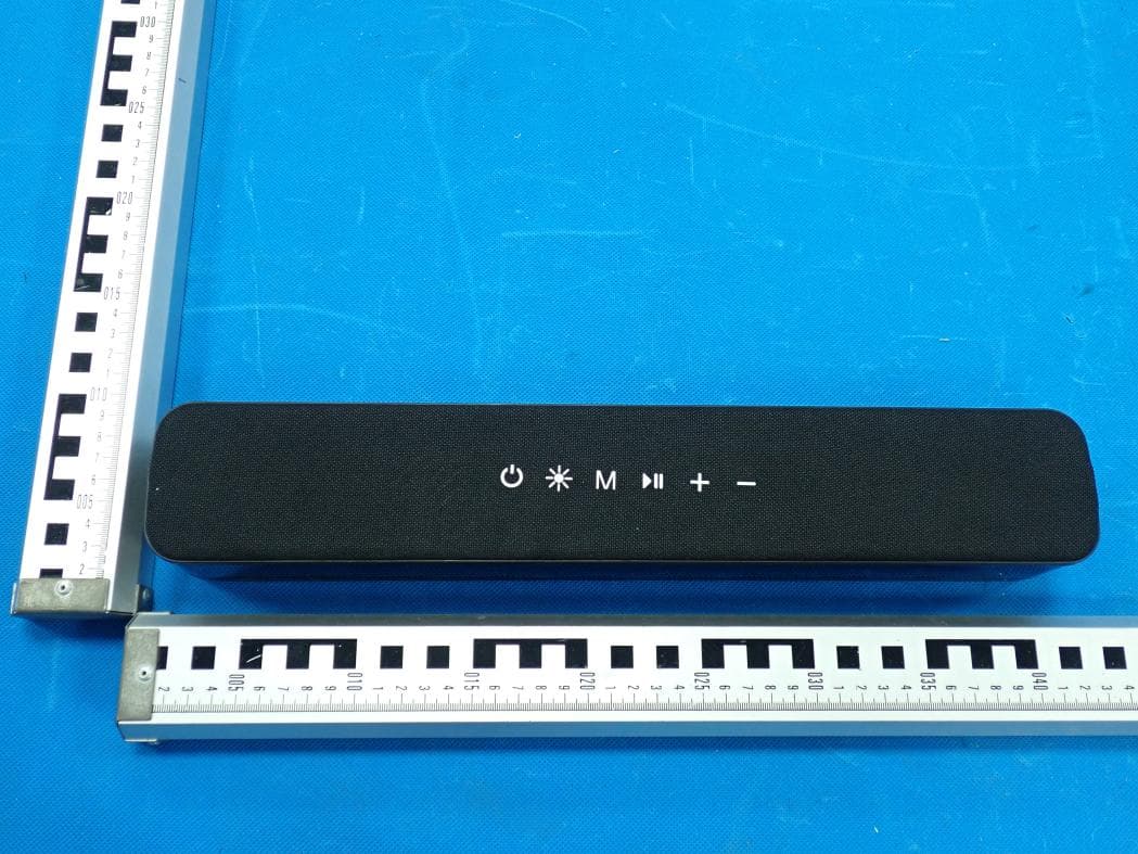
2AANZ-HYLSOBBLK
Jan 28, 2026LED Speaker Bar
Equipment Class
DSS - Part 15 Spread Spectrum Transmitter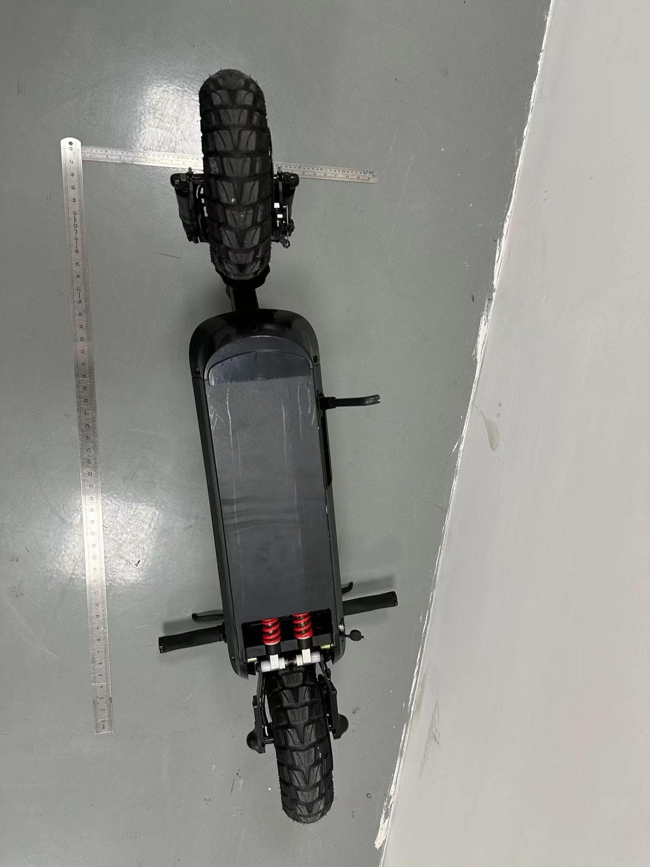
2AANZBSSDM
Oct 14, 2024HOVER-1 PRO SERIES
Equipment Class
DTS - Digital Transmission System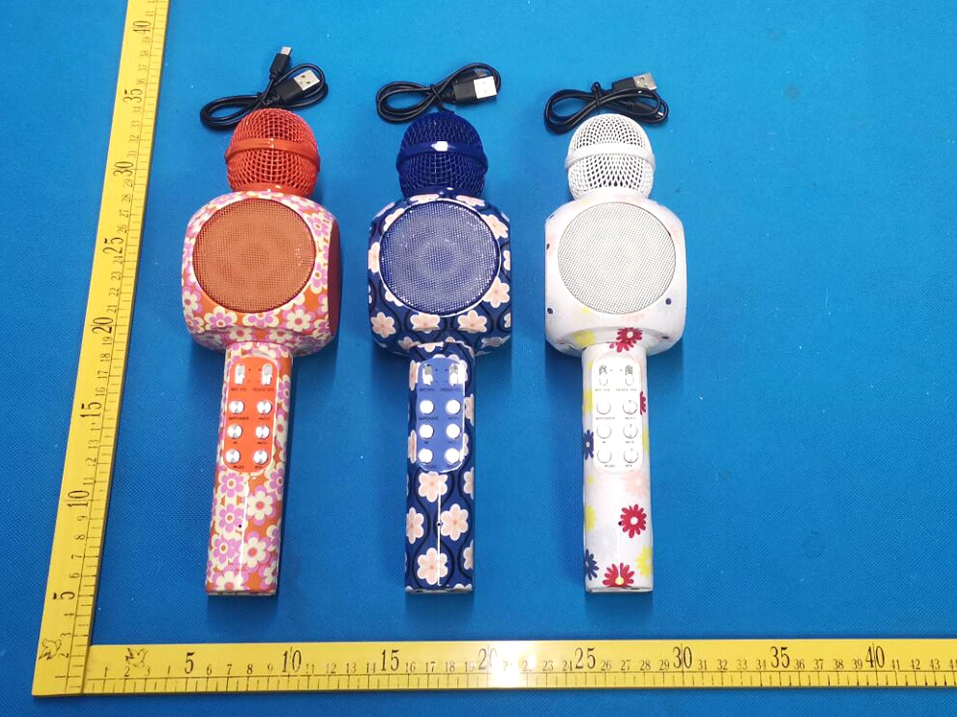
2AANZKRKFLR
Oct 10, 2024Light up Karaoke Mic with Built-in Wireless Speaker
Equipment Class
DTS - Digital Transmission System
2AANZPXLS2
Sep 26, 2024LED Pixie Light Strip
Equipment Class
DTS - Digital Transmission System
2AANZFLED1
Aug 06, 2024WIRELESS LED SPEAKER
Equipment Class
DSS - Part 15 Spread Spectrum Transmitter