2AAQS-ISP130301Bluetooth Low Energy Module
Insight SiP
Click to zoom
Application Details
- Equipment Class
- DTS - Digital Transmission System
- Date of Grant
- Jul 21, 2014
- Application Purpose
- Original Equipment
- Date of Application
- Jul 15, 2014
- Equipment Note
- Bluetooth Low Energy Module
- Frequency Range
- 2402.00000000 - 2480.00000000
- Company
- Insight SiP
- Country
- France
Documents & Files
Document Text
Text extracted from the exhibit documents filed with the FCC. Open a document above to read the original.
Users Manual
June 30, 2014 Page 1/14 Document Ref: isp_ble_DS130301_R5 Insight SiP – Green Side – 400 avenue Roumanille – BP 309 – 06906 Sophia-Antipolis Cedex – France – www.insightsip.com The information contained in this document is the property of Insight SiP and should not be disclosed to any third party without written permission. Specification subject to change without notice. BLE MODULE ISP130301 ISP130301 Bluetooth Low Energy Module with Integrated Antenna Key Features Single Mode BLE v4.0 Slave or Master Proprietary 2.4 GHz protocols Based on Nordic Semiconductor nRF51 family 2.4GHz low energy RF Transceiver 32bit ARM Cortex M0 CPU with 256kB Flash Analog and Digital peripherals Ultra Low Power Consumption Single 2.1 to 3.6 V supply Very small size 8.0 x 11.0 x 1.2 mm Temperature -25 to 75 °C Fully integrated RF matching and Antenna Integrated 16 MHz and 32.768 kHz Clocks Certifications FCC certification pending CE certification pending IC certification pending Bluetooth SIG certified RoHS compliant Applications Space constrained BLE Slave Devices Sport and fitness sensors Health care sensors Out of Range (OOR) sensors Personal User Interface Devices (PUID) Remote controls General Description This module is based on nRF51822 Nordic Semiconductor 2.4GHz wireless System on Chip (SoC) integrating a 2.4 GHz transceiver, a 32 bit ARM Cortex™-M0 CPU, a flash memory, and analog and digital peripherals. It can support BLE and a range of proprietary 2.4 GHz protocols, such as Gazell from Nordic Semiconductor. Fully qualified BLE stacks for nRF51822 are implemented in the S100 series of SoftDevices which can be freely downloaded. ISP130301 can then be used in Master and Slave modes for BLE and for both ends of other proprietary protocols. The ANT protocol can be handled on request. The module is specifically designed for both PC peripherals and ultra low power applications such as sports and wellness sensors. Ultra low power consumption and advanced power management enables battery lifetimes up to several years on a coin cell battery. Even though its very small size 8x11x1.2mm, the module integrates decoupling capacitors, 16 MHz and 32 kHz crystals, load capacitors, DC-DC converter, RF matching circuit and antenna in addition to the wireless SoC. The module forms a standalone BLE node for which only the addition of a suitable DC power source is necessary for proximity or Out of Range applications. Sensor applications require only the further addition of the appropriate sensors. As the module has several end applications, the antenna was designed to be compatible with several ground plane sizes such as USB dongle or cell phone. June 30, 2014 Page 2/14 Document Ref: isp_ble_DS130301_R5 Insight SiP – Green Side – 400 avenue Roumanille – BP 309 – 06906 Sophia-Antipolis Cedex – France – www.insightsip.com The information contained in this document is the property of Insight SiP and should not be disclosed to any third party without written permission. Specification subject to change without notice. BLE MODULE ISP130301 Contents 1. Electrical Specifications ........................................................................................................... Page 1-2 2. RF Performances .................................................................................................................... Page 1-6 3. Product Development Tools .................................................................................................... Page 1-9 4. Mechanical Outlines .............................................................................................................. Page 1-10 5. Quality & User Information ..................................................................................................... Page 1-13 6. Packaging & Storage ............................................................................................................. Page 1-14 1. Electrical Specifications Electrical Performance The specifications of the module follow those of the nRF51822. The following high level parameters are given for the module. The operating temperature range is -25 to +75 °C with the following performances. Parameter Value Unit Supply voltage Supply Voltage 2.1 to 3.6 V Current consumption Static levels Peak current, receiver active (supply at 2.1V) 12.6 mA Peak current, transmitter active +4 dBm Output Power 16 mA Peak current, transmitter active 0 dBm Output Power 10.5 mA Current drain, connection-less state 0.5 μA Current drain between connection events 2.3 μA The EUT is intended to be supplied by a current limited power source. Pin Assignment The module uses an LGA format with a double row of pads on a 0.65 mm pitch. The pad layout follows the QFN Jedec standard for 2 row LGA parts. Pads 1 thru 56 are signal pins 0.4 x 0.4 mm, Pad 57 is an exposed metal pad that is connected to ground. The NC pads are 0.8 x 0.8 or 0.4 x 0.4 mm and are to be connected to isolated metal pads on the application PCB for mechanical stability and reliability (drop test). June 30, 2014 Page 3/14 Document Ref: isp_ble_DS130301_R5 Insight SiP – Green Side – 400 avenue Roumanille – BP 309 – 06906 Sophia-Antipolis Cedex – France – www.insightsip.com The information contained in this document is the property of Insight SiP and should not be disclosed to any third party without written permission. Specification subject to change without notice. BLE MODULE ISP130301 Pin Name Pin function Description 1 P0_07 Digital I/O General purpose I/O pin 2 NC Not Connected Isolated pad on application PCB for mechanical stability 3 P0_09 Digital I/O General purpose I/O pin 4 NC Not Connected Isolated pad on application PCB for mechanical stability 5 P0_13 Digital I/O General purpose I/O pin 6 NC Not Connected Isolated pad on application PCB for mechanical stability 7 P0_19 Digital I/O General purpose I/O pin 8 NC Not Connected Isolated pad on application PCB for mechanical stability 9 P0_17 Digital I/O General purpose I/O pin 1…
Text truncated - open the document above for the full version.
Users Manual
May 20, 2014 Page 1/24 Document Ref: isp_ble_AN140101_R2 Insight SiP – Green Side – 400 avenue Roumanille – BP 309 – 06906 Sophia-Antipolis Cedex – France – www.insightsip.com The information contained in this document is the property of Insight SiP and should not be disclosed to any third party without written permission. Specification subject to change without notice. APPLICATION NOTE ISP130301-DK1 AN140101 Use of ISP130301-DK1 Introduction Scope This document gives details on hardware and software for using and testing Insight SiP Bluetooth Low Energy module ISP130301. Contents 1. Recommended Documentation ............................................................................................... Page 1-2 2. ISP130301-DK1 Hardware Content ......................................................................................... Page 1-3 3. Software Installation ................................................................................................................ Page 1-4 4. Hardware Description .............................................................................................................. Page 1-5 5. Basic Application using ISP130601 Test Board ....................................................................... Page 1-8 6. Basic Sensor Application with ISP131001 ............................................................................. Page 1-17 May 20, 2014 Page 2/24 Document Ref: isp_ble_AN140101_R2 Insight SiP – Green Side – 400 avenue Roumanille – BP 309 – 06906 Sophia-Antipolis Cedex – France – www.insightsip.com The information contained in this document is the property of Insight SiP and should not be disclosed to any third party without written permission. Specification subject to change without notice. APPLICATION NOTE ISP130301-DK1 1. Recommended Documentation The following Nordic Semiconductor documents and Dev Kits (software portion) are required to understand the complete setup and programming methods: Documents: nRF51822 Development kit User Guide (hardware section should be partially ignored – ISP development kit hardware replaces Nordic Semiconductor hardware). nRF51 Series Reference Manual. nRF51822 PS (data sheet). S110 / S120 nRF51822 SoftDevice Specification. nRF51 SDK. Dev kits (software portion): nRFgo Studio. nRF51 Software Development Kit (SDK): - Precompiled HEX files. - Source code. - Keil ARM project files. S110 / S120 nRF51822 SoftDevice. Master Control Panel. To access these files, go to www.nordicsemi.com and log in to your Nordic My Page account, enter your product key and download the files. Instructions can be found in Chapter 3. ISP documents that complement the above: AN140101 App Note – this document. DS130301 module data sheet. ISP130601 Test Board schematic SC130602. ISP131001 Sensors Board schematic SC131002. ISP130603 Interface Board schematic SC130604. May 20, 2014 Page 3/24 Document Ref: isp_ble_AN140101_R2 Insight SiP – Green Side – 400 avenue Roumanille – BP 309 – 06906 Sophia-Antipolis Cedex – France – www.insightsip.com The information contained in this document is the property of Insight SiP and should not be disclosed to any third party without written permission. Specification subject to change without notice. APPLICATION NOTE ISP130301-DK1 2. ISP130301-DK1 Hardware Content 5 x ISP130301 module samples 1 x J-Link Lite CortexM-9 JTAG/SWD Emulator 1 x nRF51822 Development Dongle (PCA10000) 1 x ISP130601 Test Board 1 x ISP131001 Sensors Board 1 x FPC jumper cable 22 pin 1 x FPC jumper cable 14 pin 1 x FPC jumper cable 10 pin 1 x 10 pin connector 1 x 2-lead patch cable 1 x Battery Holder CR2032 1 x Lithium Battery CR2032 1 x USB cable 1 x 5V power supply 1 x ISP130603 Interface Board May 20, 2014 Page 4/24 Document Ref: isp_ble_AN140101_R2 Insight SiP – Green Side – 400 avenue Roumanille – BP 309 – 06906 Sophia-Antipolis Cedex – France – www.insightsip.com The information contained in this document is the property of Insight SiP and should not be disclosed to any third party without written permission. Specification subject to change without notice. APPLICATION NOTE ISP130301-DK1 3. Software Installation This paragraph shows you the steps to follow for software installation. 1. Download and install Keil MDK-ARM Lite from https://www.keil.com/demo/eval/arm.htm to your hard drive. 2. Download and run the J-Link Software and documentation pack for Windows from http://www.segger.com/jlink-software.html. The serial number from your SEGGER J-Link hardware is needed to identify your device and can be found printed on the chip on the J-Link Lite emulator board. 3. Go to www.nordicsemi.com and log in to your Nordic My Page account. 4. Select MY KEYS from the left menu. This takes you to the My Keys page. 5. Enter the product key (included in this kit) into the Product Key field and click Add. 6. Click MY PRODUCTS in the left menu. 7. From the Add product dropdown, select the product name and click Add. The chosen product is now listed in the below Overview, My Products table. 8. In the Overview, My Products table click the Downloads link next to the product name to go directly to the relevant product page download section. 9. Download, install and run nRFgo Studio. 10. Download, install and run Master Control Panel. The software is on the CD and if you want the last version, you can find it on the Nordicsemi website. (x86 is for 32 bits windows and x64 is for 64 bits windows) 11. Download and run the nRF51 SDK installer. Make sure to choose the Keil MDK-ARM installer option. 12. Download the S110 / S120 nRF51822 SoftDevice. May 20, 2014 Page 5/24 Document Ref: isp_ble_AN140101_R2 Insight SiP – Green Side – 400 avenue Roumanille – BP 309 – 06906 Sophia-Antipolis Cedex – France – www.insightsip.com The information contained in this document is the property of Insight SiP and should not be disclosed to any third party without written permission. Specification subject to change without notice. APPLICATION NOTE ISP13030…
Text truncated - open the document above for the full version.
Cover Letter(s)
RF_734_00, Issue 1 Modular Approval Request FCC (per DA 00-1407) FCC ID: 2AAQS-ISP130301 Items to be covered Answer from applicant 1. The modular transmitter must have its own RF shielding. YES 2. The modular transmitter must have buffered modulation/data inputs (if such inputs are provided) to ensure that the module will comply with Part 15 requirements under conditions of excessive data rates or over-modulation. YES 3. The modular transmitter must have its own power supply regulation. YES 4. The modular transmitter must comply with the antenna requirements of Section 15.203 and 15.204(c). The antenna must either be permanently attached or employ a “unique” antenna coupler (at all connections between the module and the antenna, including the cable).. YES 5. The modular transmitter must be tested in a stand-alone configuration, i.e., the module must not be inside another device during testing. This is intended to demonstrate that the module is capable of complying with Part 15 emission limits regardless of the device into which it is eventually installed. YES 6. The modular transmitter must be labeled with its own FCC ID number, and, if the FCC ID is not visible when the module is installed inside another device, then the outside of the device into which the module is installed must also display a label referring to the enclosed module. This exterior label can use wording such as the following: “Contains Transmitter Module FCC ID: XYZMODEL1” or “Contains FCC ID: XYZMODEL1.” Any similar wording that expresses the same meaning may be used. The Grantee may either provide such a label, an example of which must be included in the application for equipment authorization, or, must provide adequate instructions along with the module which explain this requirement. In the latter case, a copy of these instructions must be included in the application for equipment authorization. YES 7. The modular transmitter must comply with any specific rule or operating requirements applicable to the transmitter and the manufacturer must provide adequate instructions along with the module to explain any such requirements. A copy of these instructions must be included in the application for equipment authorization. For example, there are very strict operational and timing requirements that must be met before a transmitter is authorized for operation under Section 15.231. For instance, data transmission is prohibited, except for operation under Section 15.231(e), in which case there are separate field strength level and timing requirements. Compliance with these requirements must be assured. YES 8. The modular transmitter must comply with any applicable RF exposure requirements. For example, FCC Rules in Sections 2.1091, 2.1093 and specific Sections of Part 15, including 15.319(i), 15.407(f), 15.253(f) and 15.255(g), require that Unlicensed PCS, UNII and millimeter wave devices perform routine environmental evaluation for RF Exposure to demonstrate compliance. In addition, spread spectrum transmitters operating under Section 15.247 are required to address RF Exposure compliance in accordance with Section 15.247(b)(4). Modular transmitters approved under other Sections of Part 15, when necessary, may also need to address certain RF Exposure concerns, typically by providing specific installation and operating instructions for users, installers and other interested parties to ensure compliance. YES Note: If compliance with one or more of the numbered requirements, listed above, cannot be demonstrated, it may be possible to obtain a “Limited Modular Approval” (LMA). Name and surname of applicant (or authorized representative): Imad Hjije RF_734_00, Issue 1 Date: 07\04\2014 Signature: Imad Hjije
Cover Letter(s)
FCC, Request for non-disclosure Date: 16-Jul-10 RF_501, Issue 6 Page 1 of 1 Company Name: Insight SIP Address : 13 Chemin de la halte City: Grasse Country: France To: Telefication B.V., Dept. FCC TCB Edisonstraat 12A 6902 PK ZEVENAAR The Netherlands Subject: Request for confidentiality FCC ID: 2AAQS-ISP130301 Reference number: ###### Dear FCC TCB, 1. Long-Term Confidentiality Pursuant to 47 CFR Section 0.459(a) & (b), we hereby requests non-disclosure and confidential treatment of the following materials submitted in support of FCC certification application: Bill(s) of Material Block Diagrams Operational Description Schematic Diagrams Tune-up Procedure Above materials contain secrets, proprietary and technical information, which would customarily be guarded from competitors under 47 CFR, section 0.457(d)(2). Disclosure or publication or any portion of this company confidential material to other parties could cause substantial competitive harm and provide unjustified benefits for competitors. 2. Short-Term Confidentiality (STC) Pursuant to Public Notice DA 04-1705 of the Commission’s policy, in order to comply with the marketing regulations in 47 CFR §2.803 and the importation rules in 47 CFR §2.1204, a pplicant hereby requests Short-Term Confidential treatment of the following materials (note 1): Internal Photos User’s Manual Test Set-up Photos External Photos Justification: Release of this infomration prior to the release of this product would give an unfair competitive advantage to competitors. Planned Release Date STC: 180 (notes 2, 3, 4, 5) Date: 07/21/2014 Name and signature of applicant: Imad Hjije Notes: 1) A document or type of document can only have ONE type of confidentiality! 2) Short-Term confidentiality is in principle for 45 days from date of grant; it can be extended max 3 times (total time 180 days max.)! 3) FCC must be informed when marketing begins earlier. 4) Release takes place automatically thus extension must be requested in time. Telefication does not remind you of this! 5) Request for extension or for release must be received by Telefication at least 7 days before date of actual marketing or before expiration of the STC period
ID Label/Location Info
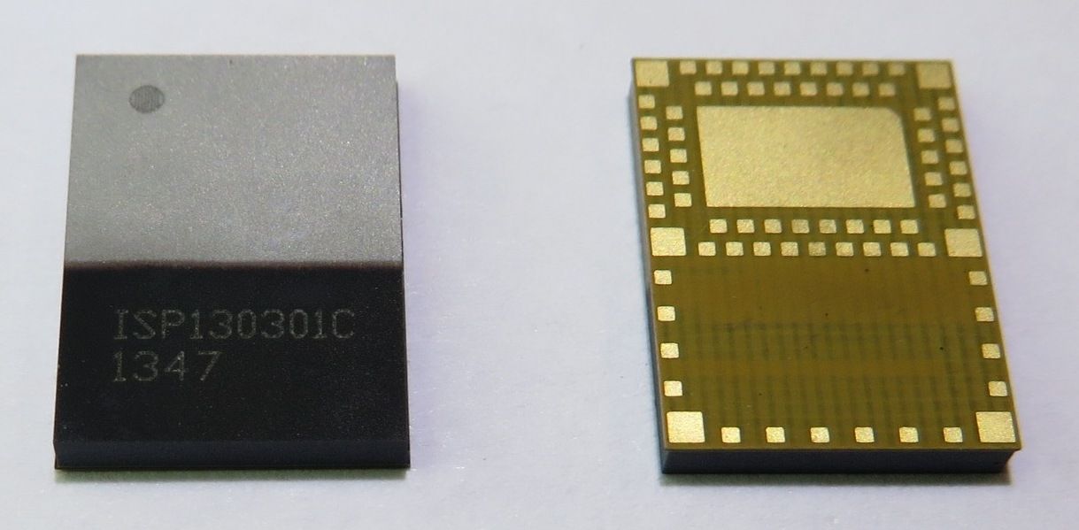
Model: ISP130301C 1347 FCC ID: 2AAQS-ISP130301 IC: 11306A-ISP130301 5 mm max
RF Exposure Info
ANNEX for SAR Excepmtion FCC ID: 2AAQS-ISP130301 IC: 11306A-ISP130301 Please find below the calculation for the EIRP value. Maximum peak output power (conducted): 2.09 dBm Antenna Gain: 0.6 dBi EIRP (calculated): 2.69 dBm = 1.857 mW
Test Report
Final Report on ISP130301 MDE_INSIGHT_1401_FCCa According to Title 47 CFR chapter I part 15 subpart C Report Reference: May 23, 2014Date: Test Laboratory: 7Layers AG Borsigstr. 11 40880 Ratingen Germany Note: The following test results relate only to the devices specified in this document. This report shall not be reproduced in parts without the written approval of the test laboratory. 7Layers AG Aufsichtsratsvorsitzender h Registergerichth registered in: Borsigstrasse 11 Chairman of the Supervisory Board: Düsseldorf, HRB 44096 40880 Ratingen, Germany Ralf Mertens USt-IdNr h VAT No.: Phone: +49 (0) 2102 749 0 Vorstandh Board: DE 203159652 Fax: +49 (0) 2102 749 350 Dr. H.-J. Meckelburg TAX No. 147/5869/0385 www.7Layers.com Reference: MDE_INSIGHT_1401_FCCa According to Title 47 CFR chapter I part 15 subpart C 2.2 Detailed Description of OUT Samples Sample : aa01 OUT IdentifierISP130301 Sample Descriptionradiated sample Low VoltageLow Temp.2.1 V-25 °C High Temp.High Voltage3.6 V+75 °C Normal Temp.Nominal Voltage3.0 V+20 °C Parameter List: ValueParameter Description Parameter for Scope FCC_v2 Always on0 Antenna Gain0.6 (dBi) Beam Gain0 (dB) Channel_BW1 (MHz) CODE000000000000 Frequency_high2480 (MHz) Frequency_low2402 (MHz) Frequency_mid2441 (MHz) Output Power_14 (dBm) Output Power_2-20 (dBm) Point to Point0 Sample : ab01 OUT IdentifierISP130301 Sample Descriptionconducted sample Low VoltageLow Temp.2.1 V-25 °C High Temp.High Voltage3.6 V+75 °C Normal Temp.Nominal Voltage3.0 V+20 °C Parameter List: ValueParameter Description Parameter for Scope FCC_v2 Always on0 Antenna Gain0.6 (dBi) Beam Gain0 (dB) Channel_BW1 (MHz) CODE000000000000 Frequency_high2480 (MHz) Frequency_low2402 (MHz) Frequency_mid2441 (MHz) Output Power_14 (dBm) Output Power_2-20 (dBm) Point to Point0 Page 4 of 36 Reference: MDE_INSIGHT_1401_FCCa According to Title 47 CFR chapter I part 15 subpart C 2.3 OUT Features Features for OUT: ISP130301 Allowed ValuesDesignationDescriptionSupported Value(s) Features for scope: FCC_v2 ACThe OUT is powered by or connected to AC Mains BTEUT supports Bluetooth data rate of 1 Mbps with GFSK modulation in the band 2400 MHz - 2483.5 MHz BTLESupport of Bluetooth Low Energy DCThe OUT is powered by or connected to DC IantIntegral Antenna: permanent fixed antenna, which may be built-in, designed as an indispensable part of the equipment TantCtemporary antenna connector, which may be only built-in for testing, designed as an example part of the equipment 2.4 Setups used for Testing For each setup a relation is given to determine if and which samples and auxiliary equipment is used. The left side list all OUT samples and the right side lists all auxiliary equipment for the given setup. Sample No.Sample DescriptionAE No.AE Description Setup No. List of OUT samplesList of auxiliary equipment AA01 aa01radiated sampleSample: AB01 ab01conducted sampleSample: 3Results 3.1 General Available at the test laboratory. The results of the inspection are described on the following pages, where 'Conformity' or 'Passed' means that the certification criteria were verified and that the tested device is conform to the applied standard. In cases where 'Declaration' is printed, the required documents are available in the manufacturers product documentation. In cases where 'not applicable' is printed, the test case requirements are not relevant to the specific equipment implementation. Documentation of tested devices: Interpretation of the test results: 1. All tests are performed under environmental conditions within the requirements of the specifications. Environmental conditions are available at the test facility. Note: Page 5 of 36 Reference: MDE_INSIGHT_1401_FCCa According to Title 47 CFR chapter I part 15 subpart C 3.2 List of the Applicable Body (Body for Scope: FCC_v2) DesignationDescription Subpart C - Intentional Radiators; 15.247 Operation within the bands 902-928 MHz, 2400-2483.5 MHz, and 5725-5850 MHz. FCC47CFRChIPART15c247RADIO FREQUENCY DEVICES 3.3 List of Test Specification Test Specification:FCC part 2 and 15 Version10-1-12 Edition Title:PART 2 - GENERAL RULES AND REGULATIONS PART 15 - RADIO FREQUENCY DEVICES Page 6 of 36 Reference: MDE_INSIGHT_1401_FCCa According to Title 47 CFR chapter I part 15 subpart C 3.4 Summary Test Case Identifier / Name SetupDate of TestResultTest (condition)Ref. Lab 15c.10 Power density §15.247 (e) 15c.10; Frequency = Low/Mid/High2014/04/16AB01Lab 1Passed 15c.11 6dB Bandwidth §15.247 (a) (2) 15c.11; Frequency = Low/Mid/High2014/04/16AB01Lab 1Passed 15c.2 Spurious radiated emissions §15.247 (d), §15.35 (b), §15.209 15c.2; Frequency = low/mid/high2014/05/14AA01Lab 1Passed 15c.4 Peak power output §15.247 (b) (1) 15c.4; Peak power output Summary2014/04/16AB01Lab 1Passed 15c.5 Spurious RF conducted emissions §15.247 (d) 15c.5; = BT transmit mode: Low/Mid/High Frequency 2014/04/16AB01Lab 1Passed 15c.6 Band edge compliance §15.247 (d) 15c.6; Band edge compliance Summary2014/04/16AB01Lab 1Passed 15c.6; Frequency = 2480, Mode = BT transmit using 1 Mbps with GFSK modulation, Method = radiated 2014/05/14AA01Lab 1Passed Page 7 of 36 Reference: MDE_INSIGHT_1401_FCCa According to Title 47 CFR chapter I part 15 subpart C 3.5 Detailed Results 3.5.1 15c.10 Power density §15.247 (e) Test: 15c.10; Frequency = Low/Mid/High Result:Passed Setup No.:AB01 Date of Test:2014/04/16 11:38 Body:FCC47CFRChIPART15c247RADIO FREQUENCY DEVICES Test Specification:FCC part 2 and 15 Page 8 of 36 Reference: MDE_INSIGHT_1401_FCCa According to Title 47 CFR chapter I part 15 subpart C Detailed Results: 2402 MHz 2426 MHz2440 MHz2480 MHz Modulation Conditions Power Density (dBm) Power Density (dBm) Power Density (dBm) Power Density (dBm) GFSK TN, VN-11.47XXX-11.97-11.23 dBm Power Density Maximum Power Density-11.23 1MAX Ref Lvl 10 dBm Ref Lvl 10 dBm RBW 3 kHz VBW 10 kHz SWT 420 ms RF Att 20 dB 2.1 dB Offset A 1MA Unit dBm 150 kHz/Center 2.402 GHzSpan 1.5 MHz EXT -80 -70 -60 -50 -40 -30 -20 -10 0 -90 10 1 Marker 1 [T1] -1…
Text truncated - open the document above for the full version.
Test Setup Photos
Test Laboratory: 7Layers AG Borsigstrasse 11 40880 Ratingen Germany Note: The following test results relate only to the devices specified in this document. This report shall not be reproduced in parts without the written approval of the test laboratory. 7 layers AG Aufsichtsratsvorsitzender h Registergerichth registered in: Borsigstrasse 11 Chairman of the Supervisory Board: Düsseldorf, HRB 44096 40880 Ratingen, Germany Peter Mertel USt-IdNr h VAT No.: Phone: +49 (0) 2102 749 0 Vorstandh Board: DE 203159652 Fax: +49 (0) 2102 749 350 Dr. H.-J. Meckelburg TAX No. 147/5869/0385 www.7Layers.com Dr. H. Ansorge Photo Report on Test Setups Report Reference: MDE_INSIGHT_1401_FCCa_Photo_Setups Test report Reference: MDE_INSIGHT_1401_FCCa_Photo_Setups Page 2 of 5 Photo 1: Test setup for radiated measurements (Enclosure, below 30 MHz, intentional radiator §15) Test report Reference: MDE_INSIGHT_1401_FCCa_Photo_Setups Page 3 of 5 Photo 2: Test setup for radiated measurements (Enclosure, semi-anechoic chamber, 30 MHz to 1 GHz, intentional radiator §15) Test report Reference: MDE_INSIGHT_1401_FCCa_Photo_Setups Page 4 of 5 Photo 3: Test setup for radiated measurements (Enclosure, fully-anechoic chamber, 1-18 GHz intentional radiator §15 / 30 MHz – 10/20 GHz §22/24/27) Test report Reference: MDE_INSIGHT_1401_FCCa_Photo_Setups Page 5 of 5 Photo 4: Test setup for radiated measurements (Enclosure, fully-anechoic chamber, 18-25 GHz, intentional radiator § 15)
Contact Information
Applicant
Philippe Genin(CEO)
Technical Contact
Non-Technical Contact
Insight SiPMichel Beghin
[email protected]33 4 9300 8882
Test Firm
7layers AGRobert Machulec
Technical Specifications
| # | Rule Parts | Frequency Range | Power Output |
|---|---|---|---|
| 1 | 15C | 2.40 GHz - 2.48 GHz | 1.60 mW |
Other Applications from Insight SiP

2AAQS-ISP5261
Mar 04, 2026Wi-Fi, BLE and Thread radio module
Equipment Class
NII - Unlicensed National Information Infrastructure TX2AAQS-ISP2454
Nov 24, 2025BLuetooth 6.0 BLE Module
Equipment Class
DTS - Digital Transmission System
2AAQS-ISP1907
Apr 22, 2021Built-in Antenna Bluetooth 5.1 Module
Equipment Class
DTS - Digital Transmission System
2AAQS-ISP4520US
Jan 14, 2021LoRa and BLE Module on small SiP package
Equipment Class
DTS - Digital Transmission System
2AAQS-ISP1807
Feb 26, 2020Bluetooth Low Energy Module
Equipment Class
DTS - Digital Transmission System