2AB5RMOD001SwipeSense Wireless module
SwipeSense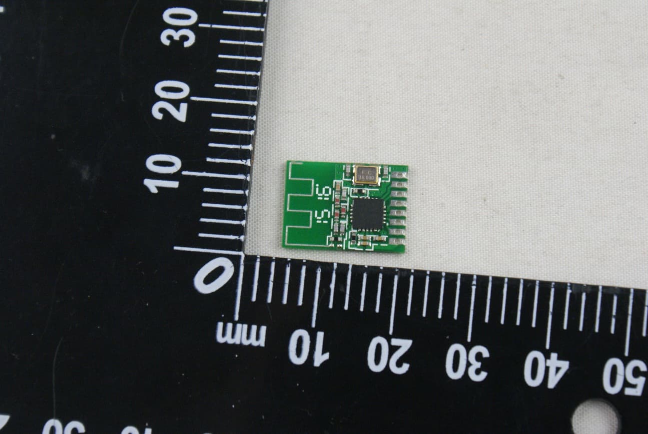
Click to zoom
Application Details
- Equipment Class
- DXX - Part 15 Low Power Communication Device Transmitter
- Date of Grant
- Jun 30, 2015
- Application Purpose
- Original Equipment
- Date of Application
- Jun 30, 2015
- Equipment Note
- SwipeSense Wireless module
- Frequency Range
- 2480.00000000 - 2480.00000000
- Company
- SwipeSense
- Country
- United States
Documents & Files
Document Text
Text extracted from the exhibit documents filed with the FCC. Open a document above to read the original.
Users Manual
SwipeSense Wireless module User Manual V1.1 Introduction: (1) Use 2.4 GHz global open ISM band free license (2) The highest working rate 2Mbps, efficient GFSK modulation, anti-interference ability, especially for industrial control occasions (3) The built-in hardware CRC error detection and point to multipoint communication control. (4 ) Low power 1.9 - 3.6V, standby mode state is 22uA; power down mode is 900nA (5 ) Built in 2.4Ghz antenna, compact size (6 ) The module can set up the address only when receiving the address of the machine to output data (provide interrupt instructions), can directly take a variety of microcontroller, software programming is very convenient (7 ) Built in specialized regulator circuit, using various power supply including DC/DC switch power supply have good communication effect (8 ) Standard DIP spacing interface, easy for embedded applications (9) Automatic packet handling, Auto packet transaction handling, With the optional built-in package response mechanism, greatly reducing the packet loss rate. (10) With the SC51 series microcontroller P0 port, the need to add 10K on the pull resistor, and the rest of the port connection do not need. (11) Other series MCU. If it is 5V, please refer to the series microcontroller IO export output current size, if exceed 10mA and need to the series resistance divider, otherwise easy to burn module! If is a 3.3V can direct and rf2401 module IO port line connection. Such as AVR series microcontroller if it is 5V, the general series of resistance 2K. Typical interface circuit: interface Introduction: (1) the range of the VCC pin is between 1.9V~3.6V and cannot be outside of the range, Over 3.6V will burn the module. Recommended voltage around 3.3V. (2) except for power VCC and ground, the rest of the foot can be directly and ordinary 5V microcontroller IO port directly connected without level conversion. Of course, about 3V microcontroller more applicable. (3) the hardware above no SPI microcontroller can also control this module, with ordinary microcontroller IO mouth simulation SPI no real serial port intervention, just ordinary single-chip IO port can, of course, with the serial port can also. (4) 9 feet grounded, and the logical connection of the motherboard; 2 feet and 9 feet vacant. (5) gill spacing of 2.54mm, standard DIP pin, if need other package interface, such as dense feet pin, or other forms of interface can contact us custom. Module structure and pin output: Msg_RF24L01 Operating mode There are four kinds of working mode: The mode of the idle mode of the transceiver mode is off mode The working mode is determined by register PRIM_RX, register PWR_UP and CE, as shown in the following table. Transceiver mode In receiving and transmitting mode enhanced shockbursttm transceiver mode, shockbursttm mode transceiver and transceiver mode three, the transceiver mode by device configuration word decision, specific configuration will be discussed in detail in the configuration part of the device. ShockBurstTM Enhanced transceiver mode Enhanced shockbursttm transceiver mode, using the first in, first out stack area and low-speed data from the microcontroller into, but a high speed (1Mbps transmission. Only in this way can try to energy-saving. Therefore, using a low speed micro controller can also get very high radio frequency data transmission rate. And RF protocol related all high-speed signal processing in tablets were, this approach has three advantages: energy saving as much as possible; low system cost (low speed microprocessor can also for high-speed RF emission); data stay in the air for a short time, anti-interference. ShockBurstTM Enhanced technology also reduces the average operating current of the whole system. In the Enhanced ShockBurstTM transceiver mode, automatic processing of NewMsg_RF24L01 prefix and CRC check code. When receiving data, automatically put the prefix and CRC check code to remove. In data transmission, automatic prefix and CRC code, in transmit mode, set the CE is high, at least 10us. When the sending process completed. Enhanced ShockBurstTM 4.1.1.1 launch process A. sends the address of the receiver and the data to send into NewMsg_RF24L01 by sequence; B. is configured for CONFIG register, so that the sending mode is sent.. C. microcontroller CE (at least 10us), Enhanced NewMsg_RF24L01 launched ShockBurstTM launch; NewMsg_RF24L01 Enhanced ShockBurstTM D. emission (1) powering the RF front end; (2) RF data package (plus prefix, CRC check code); (3) high speed emission packet; (4) the launch is complete and the NewMsg_RF24L01 enters the idle state. Enhanced ShockBurstTM 4.1.1.2 reception process A. configure the address and packet size to receive; B. configure the CONFIG register to make it into the receiving mode, the CE set high. After 130us NewMsg_RF24L01, C. enters the monitoring state, waiting for the arrival of the packet; D. when receiving a correct packet (the correct address and CRC code), NewMsg_RF2401 rf2401 automatically the prefix, address and CRC displacement; NewMsg_RF24L01 E. notify the microcontroller by setting the RX_DR (STATUS) of the STATUS register to the microcontroller interrupt.; F. microcontroller to read data from the NewMsg_RF2401; After the completion of the G. all data, you can clear the STATUS register. NewMsg_RF2401 can enter one of the four major models. ShockBurstTM transceiver mode ShockBurstTM transceiver mode can be compatible with Nrf2401a, 02, E1 and E2, NewMsg-RF2401 documents before the specific look at the company. Idle mode NewMsg_RF24L01 idle mode is designed to reduce the average operating current, the biggest advantage is that, to achieve energy saving, shorten the starting time of the chip. In idle mode, the on-chip oscillator part is still at work, the work frequency of the current with the external crystal. Shutdown mode In the shutdown mode, in order to get the minimum working current, the working current at this time is about 900nA. In the s…
Text truncated - open the document above for the full version.
Cover Letter(s)
SwipeSense, Inc. Date: Jun 17, 2015 To: Federal Communications Commission, Authorization & Evaluation Division, 7435 Oakland Mills Road, Columbia, MD 21046 RE: SwipeSense, Inc. FCC ID: 2AB5RMOD001 FCC Part 15 Certification Confidentiality Request Gentlemen: This letter is to comply with 47 CFR 0.457 and 0.459 pertaining to confidentiality material. SwipeSense, Inc. requests that the following documents regarding this submission for FCC ID: 2AB5RMOD001 be kept confidential: Exhibit Type File Name Block Diagram Block Diagram.pdf Schematics Schematics.pdf Operational Description Operational Description.pdf Those documents contain detailed system and equipment description and related information about the product which SwipeSense, Inc. considers to be confidential proprietary, a custom design and, otherwise, not releasable to the general public. Since this design is a basis form which future technological products will evolve, SwipeSense, Inc. considers this information would be of benefit to its competitors, and that the disclosure of the information in these documents would give competitors an unfair advantage in the market. Thank you for your attention to this matter. Yours Sincerely, Yuri Malina Chief Operating Officer SwipeSense, Inc.
Cover Letter(s)
SwipeSense, Inc. Date: Jun 17, 2015 To: Federal Communications Commission, Authorization & Evaluation Division, 7435 Oakland Mills Road, Columbia, MD 21046 To Whom It May Concern: The SwipeSense, Inc., the undersigned, hereby authorizes Mr. Wu Xuewen from Shenzhen Balun Technology Co., Ltd., to act on the behalf of the SwipeSense, Inc. solely in matters relating to the application for an FCC equipment authorization for FCC ID: 2AB5RMOD001 including the signing of documents in connection with this Application. Necessary acts carried out by Shenzhen Balun Technology Co., Ltd. In connection with the Application shall have the same effect as acts of the SwipeSense, Inc.. The SwipeSense, Inc. also hereby certify that no party to this application is subject to a denial of benefits, including FCC benefits, pursuant to Section 5301 of the Anti-Drug Abuse Act of 1988, 21 U.S.C. 853(a). Yours Sincerely, Yuri Malina Chief Operating Officer SwipeSense, Inc.
Cover Letter(s)
SwipeSense,Inc. Date:Jun17,2015 FederalCommunicationsCommission, Authorization&EvaluationDivision, 7435OaklandMillsRoad, Columbia,MD21046 RequestforModularApprovalFCCID:2AB5RMOD001 Item Requirements EUT Confirm (Yes/No) 1 HaveitsownRFshielding NO. ThisRFmodulewithouthisownRFshielding. NO 2 Havebufferedmodulation/datainputs(ifsuchinputs areprovided) Yes. Themodulardatainputsarebufferedthroughlogor microcontrollerconnections.Allmodulationanddatainputs arebufferedbycircuitryonthetransmitterchip. YES 3 Haveitsownpowersupplyregulation Yes. Powersupplyregulationisprovidedbycircuitryonthe transmitterchip. YES 4 Meettheantennarequirementsofsection15.203 YES ThemodularwithpermanentlyPCBantenna. YES 5 Demonstratecomplianceinastand-aloneconfiguration NO. Thismoduleissubjecttolimitedmodularapproval,during FCCtestthismodulewasbuild-inthreetypicalhosts. WearableDispenser(model:2003.0), WallSensor(model:4004.0), Badges(model:BAD001). NO 6 ThelicensedmodulemusthaveaFCCIDlabelonthe moduleitself.ThatFCCIDlabelmustbevisiblethrough awindowonthefinaldeviceoritmustbevisiblewhen anaccesspanel,doororcoveriseasilyremoved.Ifnot, asecondlabelmustbeplacedontheoutsideofthe finaldevice. YES ThemoduleislabeledwithitspermanentlyaffixedFCCID label.Thelabelpositionisclearlyindicated.Pleasereferto “labellocationphoto” YES 7 Themodulemustcomplywithallspecificrules applicabletothetransmitter.Thegranteemustprovide comprehensiveinstructionstoexplaincompliance requirements. YES Pleaserefertheusermanual. YES 8 ThemodulemustcomplywithRFexposure requirements.SeeFCCRules.SpreadSpectrum transmittersmustcomplywithRFexposurelimitsin 15.247. YES ThismoduleiscomplieswithFCC15.249RFradiatedfiled strengthlimits,setforanuncontrolledenvironment. YES Thankyouforyourattentiontothismatter. YoursSincerely, YuriMalina ChiefOperatingOfficer SwipeSense,Inc.
External Photos
ANNEX C EUT PHOTOS C.1 Appearance of the EUT THE FRONT OF EUT THE BACK OF EUT 2 / 5 THE LEFT OF EUT THE RIGHT OF EUT 3 / 5 THE UP OF EUT THE DOWN OF EUT 4 / 5 HOST 1- Badges (model: BAD001) HOST 2- Wall Sensor (model: 4004.0) 5 / 5 HOST 3- Wearable Dispenser (model: 2003.0)
ID Label/Location Info
Label: Label_location: FCCID:2AB5RMOD001
Internal Photos
ANNEX C EUT PHOTOS C.1 Appearance of the EUT THE FRONT OF EUT THE BACK OF EUT 2 / 5 THE LEFT OF EUT THE RIGHT OF EUT 3 / 5 THE UP OF EUT THE DOWN OF EUT 4 / 5 HOST 1- Badges (model: BAD001) HOST 2- Wall Sensor (model: 4004.0) 5 / 5 HOST 3- Wearable Dispenser (model: 2003.0)
Test Report
Report No.: BL-SZ1560088-601 2 Revision History Version Issue Date Revisions Rev. 01 Jun. 24, 2015 Initial Issue TABLE OF CONTENTS 1 ADMINISTRATIVE DATA (GENERAL INFORMATION) .......................................................................... 4 1.1 Identification of the Testing Laboratory .............................................................................................. 4 1.2 Identification of the Responsible Testing Location ............................................................................. 4 1.3 Announce ........................................................................................................................................... 4 2 PRODUCT INFORMATION ...................................................................................................................... 5 2.1 Applicant ............................................................................................................................................ 5 2.2 Manufacturer ...................................................................................................................................... 5 2.3 General Description for Equipment under Test (EUT) ....................................................................... 5 2.4 Technical Information ......................................................................................................................... 5 2.5 Ancillary Equipment ........................................................................................................................... 5 3 SUMMARY OF TEST RESULTS .............................................................................................................. 6 3.1 Test Standards ................................................................................................................................... 6 3.2 Verdict ................................................................................................................................................ 6 4 GENERAL TEST CONFIGURATIONS ..................................................................................................... 7 4.1 Test Environments ............................................................................................................................. 7 4.2 Test Equipment List ........................................................................................................................... 7 4.3 Test Configurations ............................................................................................................................ 8 4.4 Description of Test Setup ................................................................................................................... 8 4.4.1 For Antenna Port Test ................................................................................................................. 8 4.4.2 For AC Power Supply Port Test .................................................................................................. 8 4.4.3 For Radiated Test (Below 30 MHz) ............................................................................................. 9 4.4.4 For Radiated Test (30 MHz-1 GHz) ............................................................................................ 9 4.4.5 For Radiated Test (Above 1 GHz) ............................................................................................. 10 Report No.: BL-SZ1560088-601 3 4.5 Test Conditions ................................................................................................................................ 10 TEST ITEMS ........................................................................................................................................... 11 5.1 Antenna Requirements .................................................................................................................... 11 5.1.1 Standard Applicable .................................................................................................................. 11 5.1.2 Antenna Anti-Replacement Construction .................................................................................. 11 5.1.3 Antenna Gain ............................................................................................................................ 11 5.2 20 dB Bandwidth .............................................................................................................................. 12 5.2.1 Limit ........................................................................................................................................... 12 5.2.2 Test Procedure .......................................................................................................................... 12 5.3 Conducted Emission ........................................................................................................................ 13 5.3.1 Limit ........................................................................................................................................... 13 5.3.2 Test Procedure .......................................................................................................................... 13 5.4 Radiated Spurious Emission ............................................................................................................ 14 5.4.1 Limit ........................................................................................................................................... 14 5.4.2 Test Procedure .......................................................................................................................... 14 5.5 Band Edge ....................................................................................................................................... 15 5.5.1 Limit ........................................................................................................................................... 15 5.5.2 T…
Text truncated - open the document above for the full version.
Test Setup Photos
ANNEX B TEST SETUP PHOTOS B.1 Radiated Field Strength Measurement Below 1 GHz Below 30MHz (Host 1) Below 30MHz (Host 2) Below 30MHz (Host 3) 30 MHz-1 GHz (Host 1) 30 MHz-1 GHz (Host 2) 30 MHz-1 GHz (Host 3) Above 1 GHz 1G Hz-6 GHz (Host 1) 1G Hz-6 GHz (Host 2) 1G Hz-6 GHz (Host 3)
Contact Information
Applicant
Jeremy Jass
Test Firm
Shenzhen BALUN Technology Co.,Ltd.Xuewen Wu
Technical Specifications
| # | Rule Parts | Frequency Range | Power Output |
|---|---|---|---|
| 1 | 15C | 2.48 GHz - 2.48 GHz | - |
Other Applications from SwipeSense
2AB5RHUB521
Jul 10, 2023Location Sensor for BLE Mesh network
Equipment Class
DTS - Digital Transmission System
2AB5RSEN421
Jul 10, 2023BLE 2.4 GHz Sensor device used with BLE Mesh network
Equipment Class
DTS - Digital Transmission System
2AB5RBAD221
Jul 10, 2023BLE Mesh network device
Equipment Class
DTS - Digital Transmission System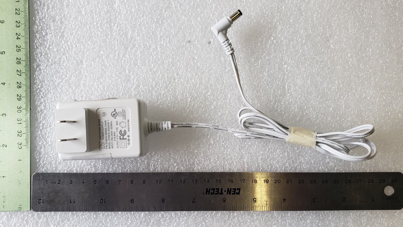
2AB5RCOM621
Jul 10, 2023BLE 2.4 GHz Communication Hub
Equipment Class
DTS - Digital Transmission System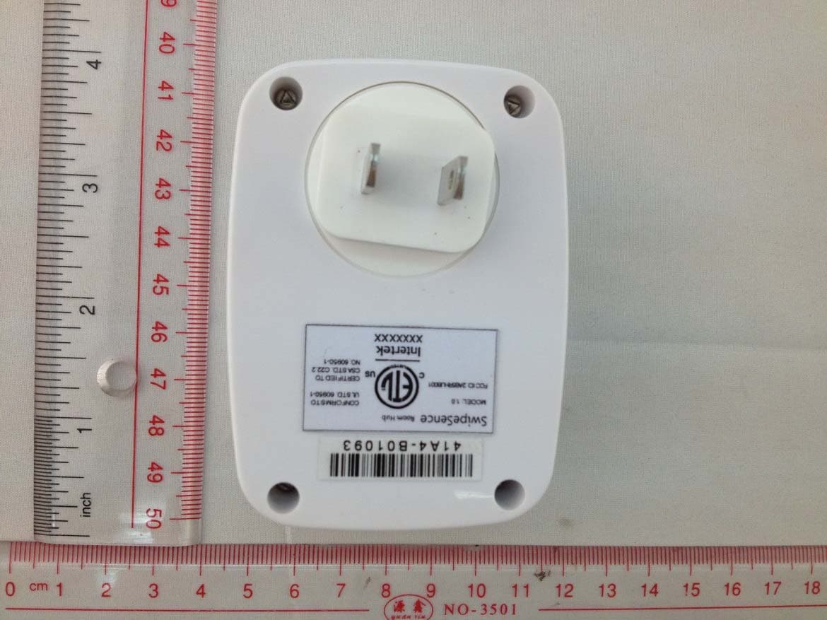
2AB5RHUB001
Jul 20, 2014Room Hub
Equipment Class
DXX - Part 15 Low Power Communication Device Transmitter