2ABRU-2564CBDE Bluetooth 5.1 Dual Mode Transceiver Module Based on CC2564C
Guangzhou BDE Technology Inc.
Click to zoom
Application Details
- Equipment Class
- DTS - Digital Transmission System
- Date of Grant
- Aug 29, 2022
- Application Purpose
- Original Equipment
- Date of Application
- Aug 29, 2022
- Equipment Note
- BDE Bluetooth 5.1 Dual Mode Transceiver Module Based on CC2564C
- Frequency Range
- 2402.00000000 - 2480.00000000
- Country
- China
Documents & Files
Document Text
Text extracted from the exhibit documents filed with the FCC. Open a document above to read the original.
Users Manual
Bluetooth 5.1 Dual Mode Transceiver Module Based on CC2564C [email protected] BDE Technology Inc. Datasheet BDE-BD2564CN 1 / 14 General Description BD2564CN is a Bluetooth 5.1 BR/EDR & LE dual mode transceiver module. The module integrates Bluetooth classic and Bluetooth Low Energy radio TI’s CC2564C, a 26-MHz crystal oscillator, a band pass filter and all the passive components at a very affordable cost. The module provides the best-in-class RF performance with transmit power and receive sensitivity that provides twice the range and higher throughput than other Bluetooth- low-energy-only solutions. The power-management hardware and software algorithms provide significant power savings in all commonly used Bluetooth BR/EDR and low energy modes of operation. The certified and royalty free Dual-mode Bluetooth 4.2 protocol stack software provides a complete Bluetooth BR/EDR, and Bluetooth Low Energy sample applications that reduce design effort and ensure a faster time to market. The module has a very small form factor with the dimensions of 7 mm x 7 mm x 1.55 mm. Key Features Bluetooth 5.1 dual mode Bluetooth Basic Rate (BR) Enhanced Data Rate (EDR) Low Energy (LE) BR and EDR features include: Up to seven active devices Scatternet: Up to three piconets simultaneously, one as master and two as slaves Up to two Synchronous Connection Oriented (SCO) links on the same piconet Support for all voice air-coding – continuously Variable Slope Delta (CVSD), A-Law, μ-Law, modified Subband Coding (mSBC), and transparent (Uncoded) Provide an assisted mode for HFP 1.6 Wideband Speech (WBS) profile or A2DP profile to reduce host processing and power Support of multiple Bluetooth profiles with enhanced QoS Low Energy features include: Multiple sniff instances tightly coupled to achieve minimum power consumption Independent buffering for Low Energy allows large numbers of multiple connections without affecting BR or EDR performance Built-In coexistence and prioritization handling for BR, EDR, and Low Energy Capabilities of link layer topology, Scatternet - can act concurrently as peripheral and central Network support for up to 10 devices Time line optimization algorithms to achieve maximum channel utilization Best-in-Class Bluetooth (RF) performance (TX power, RX sensitivity, blocking) Class 1 TX power up to +12 dBm Internal temperature detection and compensation to ensure minimal variation in RF performance over temperature, no external calibration required Improved Adaptive Frequency Hopping (AFH) Algorithm with minimum adaptation time Longer range, including twice the range of other Low-Energy-Only solutions Advanced power management for extended battery life and ease of design On-Chip power management, including direct connection to battery Low power consumption for active, standby, Bluetooth 5.1 Dual Mode Transceiver Module Based on CC2564C [email protected] BDE Technology Inc. Datasheet BDE-BD2564CN 2 / 14 and scan Bluetooth modes Shutdown and sleep modes to minimize powe consumption Physical interfaces: UART Interface with support for maximum Bluetooth data rates UART transport layer (H4) with maximum rate of 4 Mbps Three-Wire UART transport layer (H5) with maximum rate of 4 Mbps Fully programmable Digital Pulse-Code Modulation (PCM) - I2S codec interface Flexibility for easy stack integration and validation into MCUs and MPUs HCI tester tool to evaluate RF performance of the device and configure service pack Antenna: without antenna Size: 7 mm x 7 mm x 1.55 mm (With Shield) Standards Conformance Bluetooth ® SIG CE-RED (Europe) FCC (US) ISED (Canada) Japan (Telec) Bluetooth 5.1 Dual Mode Transceiver Module Based on CC2564C [email protected] BDE Technology Inc. Datasheet BDE-BD2564CN 3 / 14 Applications Mobile Accessories Sports and Fitness Applications Wireless Audio Solutions Set-Top Boxes and Remote Controls Toys Test and Measurement Industrial: Cable Replacement Wireless Sensors Automotive Aftermarket Wellness and Health Bluetooth 5.1 Dual Mode Transceiver Module Based on CC2564C [email protected] BDE Technology Inc. Datasheet BDE-BD2564CN 4 / 14 Contents General Description .............................................................................................................................................................. 1 Key Features .......................................................................................................................................................................... 1 Applications .......................................................................................................................................................................... 3 Contents ................................................................................................................................................................................ 4 1. Block Diagram ............................................................................................................................................................... 5 2. Pinout ........................................................................................................................................................................... 6 3. Characteristics .............................................................................................................................................................. 7 3.1. Absolute Maximum Ratings ............................................................................................................................. 7 3.2. Recommended Operating Conditions .............................................................................................................. 8 4. Mechanical Specifications ............................................................................................................................................ 9 4.1. Dime…
Text truncated - open the document above for the full version.
Cover Letter(s)
Agent Authorization Company: Guangzhou BDE Technology Inc. Address: B2-403, Chuangyi Building, 162 Science Avenue, Huangpu District, Guangzhou 510663, China Product Name: BDE Bluetooth 5.1 Dual Mode Transceiver Module Based on CC2564C Model Number(s): BDE-BD2564CA, BDE-BD2564CN Product Description: BDE Bluetooth 5.1 Dual Mode Transceiver Module Based on CC2564C We authorize MiCOM Labs Inc., 575 Boulder Court, Pleasanton, California 94566, USA, to act on our behalf on all matters concerning the certification of above named equipment. We declare that MiCOM Labs Inc. is allowed to forward all information related to the approval and certification of equipment to the regulatory agencies as required and to discuss any issues concerning the approval application. Any and all acts carried out by MiCOM Labs on our behalf shall have the same effect as acts of our own. Signature: Date: Aug. 24, 2022 Name: Jacky Tian Title: General Manager Company: Guangzhou BDE Technology Inc.
Cover Letter(s)
Guangzhou BDE Technology Inc. B2-403, Chuangyi Building, 162 Science Avenue, Huangpu District, Guangzhou 510663, China Office of Engineering Technology Federal Communications Commission 7435 Oakland Mills Road Columbia, MD 21046 USA Date: Aug. 24, 2022 Subject; Request for Confidentiality FCC ID: 2ABRU-2564C To Whom It May Concern, Pursuant to the provisions of the Commission’s rules Title 47 Sections §0.457 and §0.459, we are requesting the Commission to withhold the following attachment(s) as confidential documents from public disclosure indefinitely. These documents contain detailed system and equipment descriptions and are considered as proprietary information in operation of the equipment. The public disclosure of these documents might be harmful to our company and would give competitors an unfair advantage in the market. Schematic Diagram Block Diagram Operational Description Parts List Tune-up Procedure In additional to above mentioned documents, in order to comply with the marketing regulations in Title 47 CFR §2.803 and the importation rules in Title 47 CFR §2.1204, while ensuring that business sensitive information remains confidential until the actual marketing of newly authorized devices, we request Short Term Confidentiality of the following attachment(s); External Photos Test Setup Photos Internal Photos User Manual For 45 days, pursuant to Public Notice DA 04-1705. OR For 180 days pursuant to KDB 726920 D01. It is our understanding that all measurement test reports, FCC ID label format and correspondence during the certification review process cannot be granted as confidential documents and this information will be available for public review once the grant of equipment authorization is issued. Sincerely, Signature: Name: Jacky Tian Title: General Manager
Cover Letter(s)
Guangzhou BDE Technology Inc. B2-403, Chuangyi Building, 162 Science Avenue, Huangpu District, Guangzhou 510663, China Aug. 24, 2022 Office of Engineering Technology Federal Communications Commission 7435 Oakland Mills Road Columbia, MD 21046 USA Subject: Explanation of differences between product types FCC ID: 2ABRU-2564C Models: BDE-BD2564CA, BDE-BD2564CN To Whom It May Concern: We, The Guangzhou BDE Technology Inc. hereby declare that the main test module BDE-BD2564CA integrates the chip antenna, and the series module BDE-BD2564CN connects the whip antenna or chip antenna through the RF pad, and the rest are the same. Except for the different above, no other modification is performed. Sincerely, Guangzhou BDE Technology Inc. Signature: [Jacky Tian, General Manager]
Cover Letter(s)
Guangzhou BDE Technology Inc. B2-403, Chuangyi Building, 162 Science Avenue, Huangpu District, Guangzhou 510663, China RE FCC ID: 2ABRU-2564C To the certification reviewer: We are hereby applying for [full] modular approval of the above-referenced FCC ID, based on compliance with [all] of the criteria as detailed below. Sincerely, [Jacky Tian] [General Manager] Part 15 Unlicensed Single Modular Transmitter Approval Justification per 15.212 Requirement per 15.212 reference (i) The radio elements of the modular transmitter must have their own RF shielding. Shielding is provided by a metal cover over the circuitry. (ii) The modular transmitter must have buffered modulation/data inputs (if such inputs are provided. All modulation and data inputs are buffered by circuitry on the transmitter chip. (iii) The modular transmitter must have its own power supply regulation. Power supply regulation is provided by circuitry on the transmitter chip. (iv) The modular transmitter must comply with the antenna and transmission system requirements of §§ 15.203, 15.204(b) and 15.204(c). The antenna is fixed. (v) The modular transmitter must be tested in a stand-alone configuration, i.e., the module must not be inside another device during testing for compliance with Part 15 parameters. Testing was performed in a stand-alone configuration as shown in the test setup photos. (vi) The modular transmitter must be equipped with either a permanently affixed label or must be capable of electronically displaying its FCC identification number. If the FCC ID is not visible when the module is installed inside another device, then the outside of the device into which the module is installed must also display a label referring to the enclosed module. The modular was labeled with its own FCC ID. The outside of device in to which the module is installed will labeled Contains TX FCC ID: 2ABRU-2564C, Please refer to User Manual. Guangzhou BDE Technology Inc. B2-403, Chuangyi Building, 162 Science Avenue, Huangpu District, Guangzhou 510663, China (vii) The modular transmitter must comply with any specific rules or operating requirements that ordinarily apply to a complete transmitter and the manufacturer must provide adequate instructions along with the module to explain any such requirements. A copy of these instructions must be included in the application for equipment authorization. The modular is comply with all applicable FCC rules. Any modifications, not expressly approved by the manufacturer could void the authority to operate in these regions. (viii) The modular transmitter must comply with any applicable RF exposure requirements in its final configuration. This module operates under Part 15. 247 which is exempt from RF exposure evaluation owing to the very low operating power.
External Photos
Report No.: AGC02390220402AP03 Page 1 of 6 EXTERNAL PHOTOS All VIEW-1 OF EUT All VIEW-2 OF EUT Antenna 2 BDE-BD2564CA BDE-BD2564CN BDE-BD2564CN Report No.: AGC02390220402AP03 Page 2 of 6 All VIEW-3 OF EUT All VIEW-4 OF EUT Report No.: AGC02390220402AP03 Page 3 of 6 All VIEW-5 OF EUT All VIEW-6 OF EUT Antenna 3 Report No.: AGC02390220402AP03 Page 4 of 6 All VIEW-7 OF EUT Model: BDE-BD2564CA TOP VIEW OF EUT Report No.: AGC02390220402AP03 Page 5 of 6 BOTTOM VIEW OF EUT Model: BDE-BD2564CN TOP VIEW OF EUT Report No.: AGC02390220402AP03 Page 6 of 6 BOTTOM VIEW OF EUT ****************************************End of Report****************************************
ID Label/Location Info
Label Location 7mm*7mm 7mm*7mm
Internal Photos
Report No.: AGC02390220402AP03 Page 1 of 2 INTERNAL PHOTOS Model: BDE-BD2564CA INTERNAL VIEW OF EUT (FIGURE 1) INTERNAL VIEW OF EUT (FIGURE 2) Antenna 1 Report No.: AGC02390220402AP03 Page 2 of 2 Model: BDE-BD2564CN INTERNAL VIEW OF EUT (FIGURE 1) INTERNAL VIEW OF EUT (FIGURE 2) ****************************************End of Report****************************************
RF Exposure Info
RF EXPOSURE EVALUATION 1. PRODUCT INFORMATION Product Description BDE Bluetooth 5.1 Dual Mode Transceiver Module Based on CC2564C Model Name BDE-BD2564CA, BDE-BD2564CN FCC ID 2ABRU-2564C 2. EVALUATION METHOD AND LIMIT Human exposure to RF emissions from mobile devices (47 CFR §2.1091) may be evaluated based on the MPE limits adopted by the FCC for electric and magnetic field strength and/or power density, as appropriate, since exposures are assumed to occur at distances of 20 cm or more from persons. LIMITS FOR GENERAL POPULATION / UNCONTROLLED EXPOSURE Frequency Range (MHz) E-field Strength (E) (V/m) Magnetic Field Strength (H) (A/m) Power Density (S) (mW/cm 2 ) Averaging Time |E| 2 , |H| 2 or S (Minutes) 0.3 -- 1.34 614 1.63 (100)* 30 1.34 -- 30 824/f 2.19/f (180/f 2 )* 30 30 -- 300 27.5 0.073 0.2 30 300 -- 1500 -- -- f/1500 30 1500 -- 100,000 -- -- 1.0 30 *Note: 1. f= Frequency in MHz * Plane-wave Equivalent Power Density 2. The averaging time for General Population/Uncontrolled exposure to fixed transmitters is not applicable for mobile and portable transmitters. See 47 CFR §§2.1091 and 2.1093 on source-based time-averaging requirement for mobile and portable transmitters. S=PG/4πR² Where: S=power density P=power input to antenna G=power gain of the antenna in the direction of interest relative to an isotropic radiator R=distance to the center of radiation of the antenna CALCULATION A minimum test separation distance ≥ 20 cm is required between the antenna and radiating structures of the device and nearby persons to apply mobile device exposure limits. The distance must be at least 20 cm and fully supported by the operating and installation configurations of the transmitter and its antenna(s), according to the source-based time-averaged maximum power requirements of § 2.1091(d)(2). In cases where cable losses or other attenuations are applied to determine compliance, the most conservative operating configurations and exposure conditions must be evaluated. BLE: Antenna Gain=2.5dBi (Numeric 1.78), π=3.14 BR/EDR: Antenna Gain=2.5dBi (Numeric 1.78), π=3.14 Note: 1. Only the worst case recorded. Frequency Output Power Output Power Power Density Power Density Limit MHz dBm mW mW/cm 2 mW/cm 2 2480 7.881 6.14 0.0022 1 Frequency Output Power Output Power Power Density Power Density Limit MHz dBm mW mW/cm 2 mW/cm 2 2441 8.649 7.33 0.0026 1
Test Report
Page 1 of 63 FCC Test Report Report No.: AGC02390220402FE02 FCC ID : 2ABRU-2564C APPLICATION PURPOSE : Original Equipment PRODUCT DESIGNATION : BDE Bluetooth 5.1 Dual Mode Transceiver Module Based on CC2564C BRAND NAME : BDE MODEL NAME : BDE-BD2564CA, BDE-BD2564CN APPLICANT : Guangzhou BDE Technology Inc. DATE OF ISSUE : Aug. 19, 2022 STANDARD(S) : FCC Part 15.247 REPORT VERSION : V1.0 Attestation of Global Compliance (Shenzhen) Co., Ltd Report No.: AGC02390220402FE02 Page 2 of 63 REPORT REVISE RECORD Report Version Revise Time Issued Date Valid Version Notes V1.0 / Aug. 19, 2022 Valid Initial Release Report No.: AGC02390220402FE02 Page 3 of 63 TABLE OF CONTENTS 1. VERIFICATION OF COMPLIANCE ..................................................................................................................... 5 2. GENERAL INFORMATION ................................................................................................................................. 6 2.1. PRODUCT DESCRIPTION ................................................................................................................................. 6 2.2. TABLE OF CARRIER FREQUENCYS ................................................................................................................ 6 2.3. RELATED SUBMITTAL(S)/GRANT(S) ............................................................................................................... 7 2.4. TEST METHODOLOGY ...................................................................................................................................... 7 2.5. SPECIAL ACCESSORIES .................................................................................................................................. 7 2.6. EQUIPMENT MODIFICATIONS ......................................................................................................................... 7 2.7. ANTENNA REQUIREMENT ............................................................................................................................... 7 2.8. DESCRIPTION OF AVAILABLE ANTENNAS ..................................................................................................... 7 2.9. DESCRIPTION OF ANTENNA RF PORT ........................................................................................................... 8 3. MEASUREMENT UNCERTAINTY ...................................................................................................................... 9 4. DESCRIPTION OF TEST MODES .................................................................................................................... 10 5. SYSTEM TEST CONFIGURATION ................................................................................................................... 11 5.1. CONFIGURATION OF TESTED SYSTEM ....................................................................................................... 11 5.2. EQUIPMENT USED IN TESTED SYSTEM ....................................................................................................... 11 5.3. SUMMARY OF TEST RESULTS ...................................................................................................................... 11 6. TEST FACILITY ................................................................................................................................................ 12 7. PEAK OUTPUT POWER .................................................................................................................................. 13 7.1. MEASUREMENT PROCEDURE ...................................................................................................................... 13 7.2. TEST SET-UP (BLOCK DIAGRAM OF CONFIGURATION) ............................................................................. 13 7.3. LIMITS AND MEASUREMENT RESULT .......................................................................................................... 14 8. BANDWIDTH .................................................................................................................................................... 16 8.1. MEASUREMENT PROCEDURE ...................................................................................................................... 16 8.2. TEST SET-UP (BLOCK DIAGRAM OF CONFIGURATION) ............................................................................. 16 8.3. LIMITS AND MEASUREMENT RESULTS ........................................................................................................ 16 9. CONDUCTED SPURIOUS EMISSION .............................................................................................................. 20 9.1. MEASUREMENT PROCEDURE ...................................................................................................................... 20 9.2. TEST SET-UP (BLOCK DIAGRAM OF CONFIGURATION) ............................................................................. 20 9.3. MEASUREMENT EQUIPMENT USED ............................................................................................................. 20 9.4. LIMITS AND MEASUREMENT RESULT .......................................................................................................... 20 Report No.: AGC02390220402FE02 Page 4 of 63 10. MAXIMUM CONDUCTED OUTPUT POWER SPECTRAL DENSITY .............................................................. 27 10.1. MEASUREMENT PROCEDURE .................................................................................................................... 27 10.2. TEST SET-UP (BLOCK DIAGRAM OF CONFIGURATION) ........................................................................... 27 10.3. MEASUREMENT EQUIPMENT USED ........................................................................................................... 27 10.4. LIMITS AND MEASUREMENT RESULT ........................................................................................................…
Text truncated - open the document above for the full version.
Test Report
ACX Advanced Ceramic X Features Monolithic SMD with small, low-profile and light-weight type. Wide bandwidth Applications Bluetooth/Wireless LAN/Home RF ISM band 2.4GHz applications Specifications Part Number Frequency Range (MHz) Peak Gain (XZ-V) Average Gain (XZ-V) VSWR Impedance AT3216 -B2R7HAA_ 2400 ~ 2500 0.5 dBi typ. -0.5 dBi typ.2 max. 50 Ω Q’ty/Reel (pcs) : 3,000pcs Operating Temperature Range : -40 ~ +85 o C Storage Temperature Range : +5 ~ +35 o C, Humidity 45~75%RH Storage Period : 12 months max. Power Capacity : 2W max. Part Number c Type AT : Antenna d Dimensions ( L × W ) 3.2× 1.6 mm e Material Code B f Frequency Range 2R7=2700MHz g Specification Code HAA h Packaging T: Tape & Reel B: Bulk i Soldering =lead-containing /LF=lead-free Terminal Configuration No. Terminal Name No. Terminal Name c Feeding Point d NC AT3216 Series Multilayer Chip Antenna c d AT 3216 - B 2R7 HAA T /LF c d efhg i ACX Advanced Ceramic X Dimensions and Recommended PC Board Pattern Mark L W T a Dimensions 3.2±0.2 1.6±0.2 1.3+ 0.1/-0.2 0.5±0.3 (a) Without Matching Circuits (b) With Matching Circuits *Line width should be designed to match 50Ω characteristic impedance, depending on PCB material and thickness. * 2.6 4.2 1.6 1.9 0.4 Unit : mm L W a T 3.3nH 2.7nH 1.2pF ACX Advanced Ceramic X Typical Electrical Characteristics (T=25 o C) Test Board Return Loss (a) Without Matching Circuits (b) With Matching Circuits Ground 13.5mm 6.5mm 39.5mm 6.5mm Matching Circuit No Ground 50Ω Feed Line Antenna 19mm 4mm ACX Advanced Ceramic X Radiation Patterns .... XZ cut @2.45GHz Vertical Horizontal YZ cut @2.45GHz Vertical Horizontal XZ-V/XZ-H YZ-V/YZ-H XY cut @2.45GHz Vertical Horizontal XY-V/XY-H Advanced Ceramic X Corp. 16 Tzu Chiang Road, Hsinchu Industrial District Hsinchu Hsien 303, Taiwan TEL:886-3-5987008 FAX:886-3-5987001 E-mail: [email protected] http://www.acxc.com.tw 180 o 270 o 0 o 90 o X Z Y XY-cut scanning direction 180 o 270 o 0 o 90 o X Z Y XZ-cut scanning direction 180 o 270 o 0 o 90 o X Z Y YZ-cut scanning direction
Test Report
Antenna Specification 0 MANUFACTURER : Guangzhou BDE Technology Inc. DESCRIPTION : Small Size 2.4GHz Whip Antenna PART NUMBER : BDE-ANT007 Antenna Specification Antenna Specification 1 1. TECHNICAL SPECIFICATIONS Electrical Specifications Frequency Range (MHz) 2400-2500 Bandwidth (MHz) 100 Input Impendence Input Impendence (Ω) 50 V.S.W.R ≤1.7 Gain (dBi) 2.5 Polarization Type Vertical Lightning Protection DC Grounded Power Capacity (W) 50 Mechanical Specifications Antenna Length (mm) 50 Radiator Cuprum Connect Type RP-SMA-J Working Temp(°C) -40~85 Storage Temperature(°C) -20~40 Radome Color Black Radome Material TPEE Weight (g) 7.5 Antenna Specification 2 2. PRODUCT PICTURE 3. VSWR / RETURN LOSE / IMPEDANCE VSWR 50 mm RP-SMA Antenna Specification 3 RETURN LOSE IMPEDANCE Antenna Specification 4 Contact Guangzhou BDE Technology Inc. Address: B2-403, 162 Science Avenue, Huangpu District, Guangzhou 510663, China Website: www.bdecomm.com Email: [email protected] Phone: +86-20-28065335
Test Report
Integrated Antenna and RF Solutions 1 Product Specification 06MD-0002-7-PS Fusca 2.4 GHz SMD Antenna Part No. A10192 Product Specification 1 Features • Designed for 2.4 GHz applications: Bluetooth ® , Wi-Fi ® (802.11a/b/g/n), ZigBee ® , etc. as well as 2.3 GHz WiMAX ™ , 2.5 GHz WiMAX ™ and WiBro. • Easy to integrate • Low profile design for use with no ground beneath the antenna • High efficiency • Light weight • Intended for SMD mounting • Supplied in tape on reel 2 Description Fusca is intended for use with all 2.4 GHz applications. The antenna uses a ground plane in order to radiate efficiently, but this ground plane must not extend underneath the antenna itself. 3 Applications • Mobile phones • PDAs • PNDs • Headsets • PMPs / MP3s • Laptops • PC-Cards • Medical devices • Sensors Fusca 2.4 GHz SMD Antenna Part No. A10192 4 Part number Fusca: A10192 150 5 General data Product name Fusca 2.4 GHz Part Number A10192 Frequency 2.4 – 2.5 GHz Polarization Linear Operating temperature -40 ºC to +85 ºC Impedance with matching 50 Ω Weight < 0.03 g Antenna type SMD Dimensions 4 x 3 x 1.1 [mm] 6 Electrical characteristics Typical performanceConditions Peak gain 0.8 dBi Average gain -1.9 dBi Average efficiency 65% Maximum Return Loss -10 dB Maximum VSWR 2:1 All data measured on Antenova’s reference board, part number A10192-U1 Data given for the 2.4 – 2.5 GHz frequency range Integrated Antenna and RF Solutions 2 Product Specification 06MD-0002-7-PS Fusca 2.4 GHz SMD Antenna Part No. A10192 7 Electrical performance 7-1 Return Loss 2200 2300 2400250026002700 -40 -30 -20 -10 0 ∇ ∇ [MHz] [dB] 7-2 VSWR 22002300 2400250026002700 1 2 3 4 5 ∇ ∇ [MHz] Integrated Antenna and RF Solutions 3 Product Specification 06MD-0002-7-PS Fusca 2.4 GHz SMD Antenna Part No. A10192 7-3 Antenna patterns Z X Y dBi 5 -35 -15 XZ plane XY plane ZY plane Patterns show combined polarisations measured on reference board A10192-U1 Integrated Antenna and RF Solutions 4 Product Specification 06MD-0002-7-PS Fusca 2.4 GHz SMD Antenna Part No. A10192 8 Antenna dimensions Fusca L W H Length Width Height 4.0 ± 0.2 3.0 ± 0.2 1.1 ± 0.2 Dimensions in mm 9 Antenna footprint Fusca (Part No: A10192) * CAD files of the antenna footprint are available from Antenova on request. Please contact [email protected] for further details. I S O J M K 1.0 ± 0.1 0.8 ± 0.1 ≥0.9 ± 0.1 1.7 ± 0.1 0.6 ± 0.1 2.0 ± 0.1 Dimensions in mm Integrated Antenna and RF Solutions 5 Product Specification 06MD-0002-7-PS Fusca 2.4 GHz SMD Antenna Part No. A10192 10 Electrical interface 10-1 Transmission lines • All transmission lines should be designed to have a characteristic impedance of 50 Ω • The length of the transmission lines should be kept to a minimum • Any other parts of the RF system like transceivers, power amplifiers, etc, should also be designed to have an impedance of 50 Ω Once the material for the PCB has been chosen (PCB thickness and dielectric constant), a coplanar transmission line can easily be designed using any of the commercial software packages for transmission line design. For the chosen PCB thickness, copper thickness and substrate dielectric constant, the program will calculate the appropriate transmission line width and gaps on either side of the track so the characteristic impedance of the coplanar transmission line is 50 Ω. 10-2 Matching circuit The antenna requires a matching circuit that must be optimized for each customer’s product. The matching circuit will require up to three components and the following pad layout should be designed into the device so the correct circuit can be installed: The antenna feed pad is indicated in the drawing above. Additional pads are for mechanical attachment only and should not be grounded. Integrated Antenna and RF Solutions 6 Product Specification 06MD-0002-7-PS Fusca 2.4 GHz SMD Antenna Part No. A10192 In addition to the matching circuit, a separate DC blocking capacitor will also be required between the radio and the antenna matching circuit. Note: The component values for the matching circuit will vary depending on the size of the PCB and surrounding components. The impedance of the antenna should be measured before selecting suitable matching components. Antenova offers this service on request. Contact [email protected] for further information. 10-3 Antenna placement Antenova strongly recommends placing the antenna near the edge of the board. Maximum antenna performance is achieved by placing the antenna towards one of the corners of the PCB and with the feed point of the antenna as close to same corner of the PCB as possible. Additional ground and components near the antenna should be at a distance of at least 2 mm. Where possible the antenna should be clear of ground from both sides, although the antenna can work well with a minimum clearance of D ≥ 2 mm as shown in the drawing above. Integrated Antenna and RF Solutions 7 Product Specification 06MD-0002-7-PS Fusca 2.4 GHz SMD Antenna Part No. A10192 10-4 Reference boards The reference board has been designed for evaluation purposes of Fusca 2.4 GHz and it includes a SMA female connector Fusca Dimensions in mm To order a reference board c…
Text truncated - open the document above for the full version.
Contact Information
Applicant
Jacky Tian
Technical Contact
Test Firm
Attestation of Global Compliance (Shenzhen) Co., LDoris Li
[email protected]+86-755-25234088
Technical Specifications
| # | Rule Parts | Frequency Range | Power Output |
|---|---|---|---|
| 1 | 15C | 2.40 GHz - 2.48 GHz | 6.10 mW |
Other Applications from Guangzhou BDE Technology Inc.

2ABRU-WF3235
Sep 21, 2022BDE Dual-Band WiFi MCU Module
Equipment Class
DTS - Digital Transmission System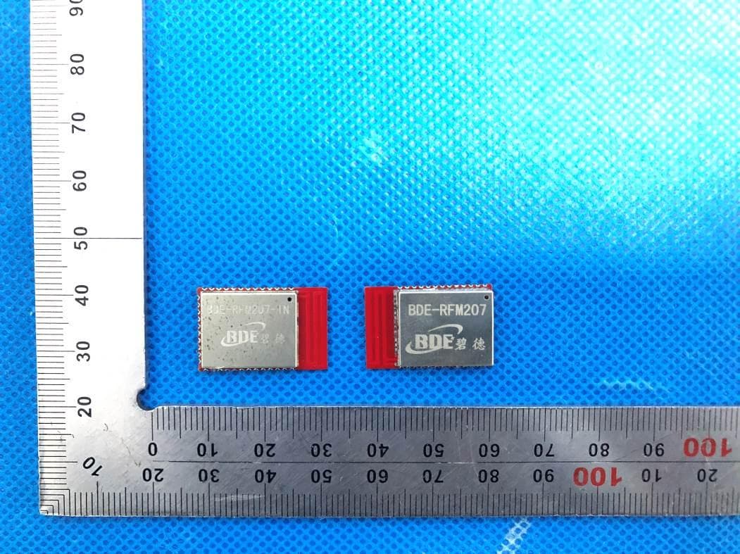
2ABRU-RFM207
May 13, 2021Multiprotocol 2.4G Wireless Module - Industrial Grade
Equipment Class
DTS - Digital Transmission System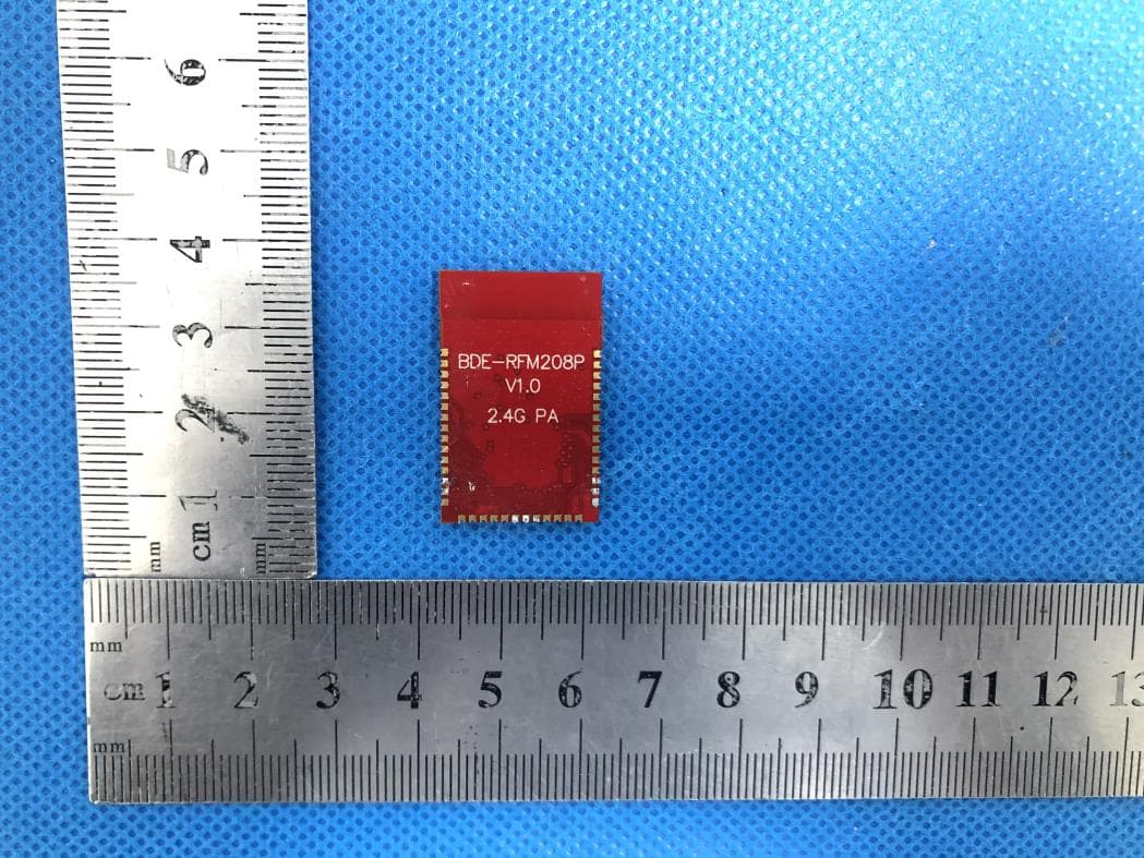
2ABRU-RFM208P24
May 12, 2021Multi-Band Wireless Module with PA
Equipment Class
DTS - Digital Transmission System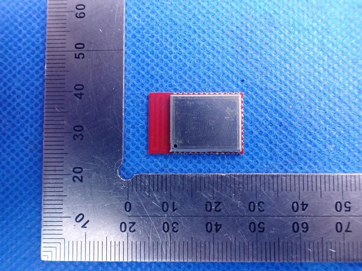
2ABRU-RFM207B
Apr 27, 2021Multiprotocol 2.4G Wireless Module - Industrial Grade
Equipment Class
DTS - Digital Transmission System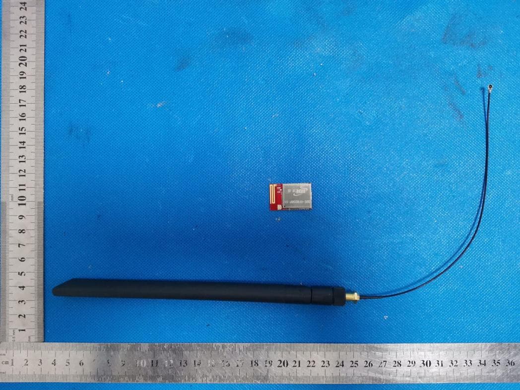
2ABRU-RFM208PS1
Apr 24, 2021Multi-Band Wireless Module with PA
Equipment Class
DTS - Digital Transmission System