2ACUJR4274K-Band Doppler Sensing Device (Movement Sensor)
Nisshinbo Micro Devices Inc.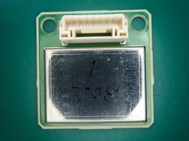
Click to zoom
Application Details
- Equipment Class
- DXX - Part 15 Low Power Communication Device Transmitter
- Date of Grant
- Feb 17, 2022
- Application Purpose
- Original Equipment
- Date of Application
- Feb 16, 2022
- Equipment Note
- K-Band Doppler Sensing Device (Movement Sensor)
- Frequency Range
- 24057.00000000 - 24244.00000000
- Company
- Nisshinbo Micro Devices Inc.
- Country
- Japan
Documents & Files
Document Text
Text extracted from the exhibit documents filed with the FCC. Open a document above to read the original.
Users Manual
Date January 24,2022 Specifications / User Manual 24GHz Sensor Module Model No. NJR4274 Copyright © Nisshinbo Micro Devices Inc. Microwave Business Headquarters -Notice of Proprietary Information- This document and contents are proprietary to Nisshinbo Micro Devices Inc. This publication and contents may not be reproduced or distributed for any other purpose without the written permission of Nisshinbo Micro Devices Inc. Specifications listed in this document are subject to change at any time, without notice. Nisshinbo Micro Devices Inc. Microwave Business Headquarters Title: Specifications of NJR4274 for Radio Certification Reference No.: PDS-R4274 Rev.: 00-06E Sheet: 1 / 14 For Radio Certification NJR4274 *Above specifications are subject to change without notice. Reference No.: PDS-R4274 Rev.: 00-06E Sheet: 2 Scope NJR4274 K-band (24GHz) Doppler Module has been designed for motion sensing applications. Main Structure Integrated antenna structure, the patch antenna is integrated on the module PCB. All of electric parts except interface connector are covered with metal cap. Operation Overview 5 V input operation, LDO integrated. Implemented an internal MCU for RF frequency tuning of RF-IC and intermittent-operation. Internal MCU controls ON/OFF of Output voltage from LDO which connect to the input voltage terminal of RF IC. This module is 2-frequencies CW (FSK) type sensor that can simultaneously measure the distance and velocity of the moving target. It operates duty cycle of intermittent-operation has 2-operation- mode (Normal operation mode / Low power operation mode). 2-operation-mode are different duty cycle. (refer Fig.2) RF frequency is output during ON time. Internal MCU supplies the tuning voltage to RFIC and the RF frequency is controlled by tuning voltage. Since the RF frequency is switched every intermittent-operation cycle, the tuning voltage is switched every cycle. Switched RF frequency is 2-frequencies, and difference of those 2-frequencies is 15 MHz +/- 3 MHz. Fig.1 Functional Block Diagram NJR4274 *Above specifications are subject to change without notice. Reference No.: PDS-R4274 Rev.: 00-06E Sheet: 3 Electrical Specifications ITEM MIN. TYP. MAX. UNITS REMARKS 1.1. Power Supply (1) Operating Voltage 4.75 5 5.25 V (2) Operating Current Normal Operation Mode ― ― 50 mA Low Power Mode ― ― 6 mA 1.2. RF Parameter (1) RF Frequency (Transmission) for US, Canada, Taiwan and Korea 24.05 ― 24.25 GHz Refer Chart 1. (2) Transmission Operation Mode 2-Frequencies CW(FSK) (3) Frequency Difference of FSK ― 15 ― MHz (4) Output Power ― 1.8 ― dBm (5) E.I.R.P. ― ― 10 (10) mW (dBm) (7) Spurious Emission ― ― 2,500 uW/m (8) Antenna. Antenna Gain ― 6.5 6.7 dBi -3dB beam width / Horizontal ― 45 ― deg. -3dB beam width / Vertical ― 40 ― deg. NJR4274 *Above specifications are subject to change without notice. Reference No.: PDS-R4274 Rev.: 00-06E Sheet: 4 Chart 1. Frequency Channel List NJR4274 *Above specifications are subject to change without notice. Reference No.: PDS-R4274 Rev.: 00-06E Sheet: 5 Normal Operation Mode Notes: In normal mode, the modules transmit alternately at frequencies F1 and F2. A period of F1 and F2 has each 500us. Both transmit ON-time is 47us, OFF-times is 453us. F2 is started to transmit delayed 250us after F1 transmit. Low Power Operation Mode Notes: In Low Power Operation mode, the modules transmit alternately at frequencies F1 and F2. A period of F1 and F2 has each 10ms nominal, range 9 to 11ms. Both transmit ON-time is 47us, F2 is started to transmit delayed 250us after F1 transmit. Fig.2 Frequency Time Chart NJR4274 *Above specifications are subject to change without notice. Reference No.: PDS-R4274 Rev.: 00-06E Sheet: 6 1. Environmental Specifications ITEM SPECIFICATION Operation Temperature -10 to +41 °C Storage Temperature -30 to +70 °C Humidity 0 to 64 % @+41 °C NJR4274 *Above specifications are subject to change without notice. Reference No.: PDS-R4274 Rev.: 00-06E Sheet: 7 2. Drawing 2.1. Outline 2.2. Interface (1) Connector: BM07B-GHS-TBT / J. S. T. MFG. CO., LTD. (2) Pin Assignment # NAME I/O DESCRIPTION 1 Vcc I +5 V Input 2 TxD O Serial Communication Tx Port 3 RxD I Serial Communication Rx Port 4 GND ― GND 5 TxD O Serial Communication Internal AD value is output 6 N/A I Do not connect, Internal Usage 7 N/A I Do not connect, Internal Usage NJR4274 *Above specifications are subject to change without notice. Reference No.: PDS-R4274 Rev.: 00-06E Sheet: 8 2.3. Label Drawing NJR4274 *Above specifications are subject to change without notice. Reference No.: PDS-R4274 Rev.: 00-06E Sheet: 9 1. Nissinbo Micro Devices strives to produce reliable and high quality microwave components. Nissinbo Micro Devices's microwave components are intended for specific applications and require proper maintenance and handling. To enhance the performance and service of Nissinbo Micro Devices's microwave components, the devices, machinery or equipment into which they are integrated should undergo preventative maintenance and inspection at regularly scheduled intervals. Failure to properly maintain equipment and machinery incorporating these products can result in catastrophic system failures. 2. To ensure the highest levels of reliability, Nissinbo Micro Devices products must always be properly handled. The introduction of external contaminants (e.g. dust, oil or cosmetics) can result in failures of microwave components. 3. Nissinbo Micro Devices offers a variety of microwave components intended for particular applications. It is important that you select the proper component for your intended application. You may contact Nissinbo Micro Devices 's sales office or sales representatives, if you are uncertain about the products listed in the catalog and the specification sheets. 4. Special care is required in designing devices, machinery or equipment, which demand high levels of reliability. This is particularly important when designing critical components or syst…
Text truncated - open the document above for the full version.
External Photos
Label NJR4274 External Photo Diagrammatic perspective view Front Side view: Patch Antenna Back Side view: Metal Shielding Cover
ID Label/Location Info
Material: PET Adhesive compound: PA-T1 (acrylic ester) Life time: over 10years NJR4274 Label Label Design Label Location There is no specification of the label sticking direction NJR4274 001- A18838 R-R-NJR- NJR4274 CCAN21Y11260T3
Internal Photos
NJR4274 Internal Photo Without Metal Shielding Cover
RF Exposure Info
FCC ID: 2ACUJR4274 Prüfbericht - Produkte Test Report - Products RF Exposure Statement: JP2125FA 003 Seite 1 von 2 Page 1 of 2 Client: Nisshinbo Micro Devices Inc. (*) 1-1, Fukuoka 2-Chome, Fujimino-City, Saitama, 356-8510 Japan Test item: K-Band Doppler Sensor Module (Movement Sensor) Identification: NJR4274 FCC Requirement According to FCC §2.1093 (d)(1), Portable Devices that transmit at frequencies above 6 GHz must comply with the following applicable limit for maximum permissible exposure (MPE) specified in FCC §1.1310 (e)(1), Table 1: Equipment Use Frequency Range [MHz] Power Density Limit Average Time [min] General Population / Uncontrolled Exposure 1,500 – 100,000 1.0 [mW/cm 2 ] <30 Note: This evaluation was conducted at 2cm test separation distance (variable r in the statement). It was specified by the customer. Measurement Result The maximum measured E-field strength and corresponded estimated EIRP from the transmitter are given in the following table: Freq. [GHz] Wave Length [cm] Measured E-Field Strength E Meas. Distance R [m] Calculated EIRP Test Distance r [cm] Calculated Power Density S [mW/cm 2 ] [dBuV/m] [V/m] [mW] [dBm] 24.17122870 1.2411 80.47 0.0106 3.0 0.033708 -14.723 2.0 0.000671 Note: The EIRP in mW is calculated in conjunction with the following formula: EIRP = (E × R) 2 /30 = (0.0106 × 3.0) 2 / 30 = 0.000033708 [W] = 0.033708 [mW] TÜV Rheinland Japan Ltd. – Global Technology Assessment Center 4-25-2 Kita-Yamata, Tsuzuki-ku, Yokohama 224-0021, Japan FCC ID: 2ACUJR4274 Prüfbericht - Produkte Test Report - Products RF Exposure Statement: JP2125FA 003 Seite 2 von 2 Page 2 of 2 The power density S in mW/cm 2 is calculated in conjunction with the next formula: S = EIRP / (4 × π × r 2 ) = 0.033708 / (4 ×π × 2.0 2 ) = 0.000671 [mW/cm 2 ] Since the shortest wave length λ of transmitter is 1.2411cm, above mentioned calculations are considered in far field condition. Normal mode is the worst case configuration of this transmitter, therefore above mentioned condition is considered as the most severe estimation. For details, refer to the relevant sections that is submitted test report, JP216XYU 002. Conclusion This transmitter module is classified as Portable Devices by the client. SAR evaluation is not required since nominal frequency of the transmitter is higher than 6GHz, therefore, RF exposure evaluation (MPE) was conducted by the above-mentioned calculated method. As a result, calculated Power Density S is below FCC limit at the separation distance of 2cm. Note: This RF Exposure Evaluation (JP2125FA 003) replaces the original evaluation (JP2125FA 001). (*) Former New Japan Radio Co., Ltd. TÜV Rheinland Japan Ltd. – Global Technology Assessment Center 4-25-2 Kita-Yamata, Tsuzuki-ku, Yokohama 224-0021, Japan
Test Report
FCC ID: 2ACUJR4274 IC: 22589 -R4274 Prüfbericht - Produkte Test Report - Products TÜV Rheinland Japan Ltd. x Global Technology Assessment Center x 4-25-2 Kita-Yamata x Tsuzuki-ku x Yokohama 224-0021 x Japan Tel.: +81 45 914 3888 x Mail: [email protected] x Web: www.tuv.com Prüfbericht-Nr.: Test Report No.: JP216XYU 002 Auftrags-Nr.: Order No.: 150245576 Seite 1 von 55 Page 1 of 55 Kunden-Referenz-Nr.: Client Reference No.: N/A Auftragsdatum: Order Date: 2021-07-30 Auftraggeber: Client: New Japan Radio 1-1, Fukuoka 2-Chome Fujimino City Saitama, 356-8510 Japan Prüfgegenstand: Test Item: K-Band Doppler Sensor Module (Movement Sensor) Bezeichnung / Typ-Nr.: Identification / Type No.: NJR4274 Serien-Nr.: Serial No.: Sample01 Auftrags-Inhalt: Order C ontent: Radio Testing Prüfgrundlage: Test Specification: FCC 47 CFR Part 15, Subpart C, Section 15.249 ANSI C63.10-2013 RSS-Gen (Issue 5): 2018+Amendment 1:2019 RSS-210 (Issue 10): 2019+Amendment 1:2020 ANSI C63.10-2013 Wareneingangsdatum: Date of Receipt: 2021-09-14 -/- Prüfmuster-Nr.: Test Sample No.: A003093437, A003095132 Prüfzeitraum: Testing Period: 2021-09-14 to 2021-12-20 Ort der Prüfung: Place of Testing: Yokohama EMC Laboratory Prüflaboratorium: Testing Laboratory: TÜV Rheinland Japan Ltd. Prüfergebnis*: Test Result*: Pass zusammengestellt von: compiled by : Datum: Date: 2021-12-23 Takeshi Nagata Stellung / Position: Inspector genehmigt von: authorized by : Ausstellungsdatum: Issue date: 2021-12-23 Pin Zhang Stellung / Position: Reviewer Sonstiges / Other: Zustand des Prüfgegenstandes bei Anlieferung: Condition of the Test Item at Delivery: Prüfmuster vollständig und unbeschädigt Test item complete and undamaged * Legende: P(ass) = entspricht o.g. Prüfgrundlage(n) F(ail) = entspricht nicht o.g. Prüfgrundlage(n) N/A = nicht anwendbar N/T = nicht getestet * Legend: P(ass) = passed a.m. test specification(s) F(ail) = failed a.m. test specification(s) N/A = not applicable N/T = not tested Dieser Prüfbericht bezieht sich nur auf das o.g. Prüfmuster und darf ohne Genehmigung der Prüfstelle nicht auszugsweise vervielfältigt werden. Dieser Bericht berechtigt nicht zur Verwendung eines Prüfzeichens. This test report relates to the a. m. test sample. Without permission of the test center this test report is not permitted to be duplicated in extracts. This test report does not entitle to carry any test mark. FCC ID: 2ACUJR4274 IC: 22589 -R4274 Prüfbericht - Produkte Test Report - Products Prüfbericht-Nr.: Test Report No.: JP216XYU 002 Seite 2 von 55 Page 2 of 55 REVISIONS Report No. Issue date Changes / Remarks JP216XYU 001 2021-11-18 Original document (Test report for Intentional radiator aspects) JP216XYU 002 2021-12-23 Additional testing for fundamental FCC ID: 2ACUJR4274 IC: 22589 -R4274 Prüfbericht - Produkte Test Report - Products Prüfbericht-Nr.: Test Report No.: JP216XYU 002 Seite 3 von 55 Page 3 of 55 Contents 1. GENERAL REMARKS ................................................................................................ 5 1.1 TEST SPECIFICATIONS ............................................................................................. 5 1.2 COMPLEMENTARY MATERIALS ................................................................................. 6 2. TEST SITES ............................................................................................................. 7 2.1 TEST FACILITIES ..................................................................................................... 7 2.2 LIST OF TEST AND MEASUREMENT INSTRUMENTS ...................................................... 7 2.3 MEASUREMENT UNCERTAINTY ................................................................................. 9 3. GENERAL PRODUCT INFORMATION ......................................................................... 10 3.1 PRODUCT FUNCTION AND INTENDED USE ................................................................ 10 3.2 RATINGS AND SYSTEM DETAILS ............................................................................. 10 3.3 NOISE GENERATING AND NOISE SUPPRESSING PARTS............................................. 11 3.4 SUBMITTED DOCUMENTS AND INFORMATION ........................................................... 11 4. TEST SETUP AND OPERATION MODES .................................................................... 12 4.1 TEST METHODOLOGY ............................................................................................ 12 4.2 OPERATION MODES............................................................................................... 12 4.3 PHYSICAL CONFIGURATION FOR TESTING ............................................................... 12 4.4 TEST SOFTWARE ................................................................................................... 14 4.5 SPECIAL ACCESSORIES AND AUXILIARY EQUIPMENT................................................ 14 4.6 COUNTERMEASURES TO ACHIEVE COMPLIANCE ....................................................... 15 5. TEST RESULTS R AD I O .................................................................................... 16 5.1 TECHNICAL REQUIREMENTS ................................................................................... 16 5.1.1 Supply Voltage Requirements .................................................................................................... 16 5.1.2 Antenna Requirements .............................................................................................................. 16 5.1.3 Restricted Bands of Operation ................................................................................................... 17 5.2 RADIATED MEASUREMENTS ................................................................................... 18 5.2.1 Duty Cycle .................................................................................................................................. 18 5.2.2 20dB Bandwidth ...................................................…
Text truncated - open the document above for the full version.
Test Setup Photos
FCC ID: 2ACUJR4274 IC: 22589 -R4274 Prüfbericht - Produkte Test Report - Products Prüfbericht-Nr.: Test Report No.: JP216XYU 002 Seite 48 von 55 Page 48 of 55 6. Photographs of the Test Setup Photograph 1: Set-up for AC Power Line Conducted Emission, Front View Photograph 2: Set-up for AC Power Line Conducted Emission, Rear View FCC ID: 2ACUJR4274 IC: 22589 -R4274 Prüfbericht - Produkte Test Report - Products Prüfbericht-Nr.: Test Report No.: JP216XYU 002 Seite 49 von 55 Page 49 of 55 Photograph 3: Set-up for Radiated Emission below 1GHz, Front View Photograph 4: Set-up for Radiated Emission below 1GHz, Rear View FCC ID: 2ACUJR4274 IC: 22589 -R4274 Prüfbericht - Produkte Test Report - Products Prüfbericht-Nr.: Test Report No.: JP216XYU 002 Seite 50 von 55 Page 50 of 55 Photograph 5: Set-up for Radiated Emission above 1GHz, Front View Photograph 6: Set-up for Radiated Emission above 1GHz, Rear View FCC ID: 2ACUJR4274 IC: 22589 -R4274 Prüfbericht - Produkte Test Report - Products Prüfbericht-Nr.: Test Report No.: JP216XYU 002 Seite 51 von 55 Page 51 of 55 Photograph 7: Set-up for Radiated Emission above 40GHz, Front View Photograph 8: Set-up for X-Axis of the EUT FCC ID: 2ACUJR4274 IC: 22589 -R4274 Prüfbericht - Produkte Test Report - Products Prüfbericht-Nr.: Test Report No.: JP216XYU 002 Seite 52 von 55 Page 52 of 55 Photograph 9: Set-up for Y-Axis of the EUT Photograph 10: Set-up for Z-Axis of the EUT FCC ID: 2ACUJR4274 IC: 22589 -R4274 Prüfbericht - Produkte Test Report - Products Prüfbericht-Nr.: Test Report No.: JP216XYU 002 Seite 53 von 55 Page 53 of 55 Photograph 11: EUT Antenna side Metal cap side Photograph 12: Evaluation Board
Contact Information
Applicant
Yuji Kita(Microwave QA Manager)
Technical Contact
TUV Rheinland Japan Ltd.Akira -/- Abe
[email protected]81459140538
Global Technology Assessment Center · Yokohama · Japan
Test Firm
TUV Rheinland Japan Ltd., Global Technology AssessMinoru Yamanaka
Technical Specifications
| # | Rule Parts | Frequency Range | Power Output |
|---|---|---|---|
| 1 | 15C | 24.06 GHz - 24.24 GHz | - |
Other Applications from Nisshinbo Micro Devices Inc.
2ACUJR4269
Aug 31, 2015K-Band Doppler Sensor Module (Movement Sensor)
Equipment Class
FDS - Part 15 Field Disturbance Sensor
2ACUJR4262
Jan 19, 2015K-Band Doppler Sensor Module (Movement Sensor)
Equipment Class
FDS - Part 15 Field Disturbance Sensor