2ADLXS1150SL00Wearable bio-sensing device
TDK Corporation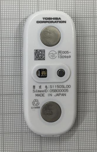
Click to zoom
Application Details
- Equipment Class
- DSS - Part 15 Spread Spectrum Transmitter
- Date of Grant
- Apr 16, 2015
- Application Purpose
- Original Equipment
- Date of Application
- Apr 15, 2015
- Equipment Note
- Wearable bio-sensing device
- Frequency Range
- 2402.00000000 - 2480.00000000
- Company
- TDK Corporation
- Country
- Japan
Documents & Files
Document Text
Text extracted from the exhibit documents filed with the FCC. Open a document above to read the original.
Users Manual
●To use the product correctly and safely, read and fully understand the instruction manual before attempting to use the product. ●After reading the instruction manual, store it in a safe place so that whoever will later use the product can reference it at any time. ●Procedures, screen shots and illustrations contained in the instruction manual may be modifi ed without prior notice. ■ Trademarks • Silmee TM is a registered trademark of TOSHIBA Corporation. • Android TM is a registered trademark of Google Inc. • Bluetooth ® word mark and logo are owned by Bluetooth SIG, Inc. and licensed for use by TOSHIBA Corporation. • Other product and system names described in this document may be used as registered trademarks or trademarks by the respective owners. Safety Precautions Be sure to observe the following precautions: This section lists important precautions which users of this product (and anyone else) should observe in order to avoid injury to human body and damage to property, and to ensure safe and correct use of the product. Please be sure that you understand the meanings of the labels and graphic symbols described below before you move on to the detailed descriptions of the precautions, and comply with the precautions stated. ■ Explanation of labels Label Description Indicates a potentially hazardous situation that may lead to serious injury or death if the precaution is not followed. Indicates a potentially hazardous situation that may lead to minor or moderate injury if the precaution is not followed. Indicates a situation that could lead to property damage if the precaution is not followed. ■ Explanation of graphic symbols Graphic symbol Description Prohibited indicates prohibited actions. Specifi c actions to be prohibited are indicated within or near the graphic symbol using an appropriate picture or text. Instructions indicates actions which must be undertaken for safety purposes. Specifi c actions to be undertaken are indicated within or near the graphic symbol using an appropriate picture or text. To prevent injury Proper operation and storage To prevent damage Instructions Stop using this product immediately if the dedicated cradle becomes hot during charging. This may damage the product or cause it to catch fi re. Prohibited Do not disassemble, repair or modify the product. Such an attempt may cause a failure or damage to the product. For repairing the product or replacing the battery, contact TOSHIBA by referring to “Contact Information” on the back cover. Do not drop, step on or otherwise apply a strong shock to the product. Such an attempt may cause the product to fail or malfunction. Such damage to equipment may also reduce its waterproofness. Do not intentionally splash water on the product, sink it in water, or get in the water wearing it. Such an attempt may cause a failure of the product. Although the Silmee Bar type Lite is waterproof against splashes of water occurring in daily life (such as sweat or splashes occurring when you are washing your face) as well as splashes caused by rain, it cannot be used in any situation where it may be severely splashed, such as washing the product, bathing or taking a shower wearing it. Furthermore, accessories are not waterproof. Do not charge any product other than Silmee Bar type Lite in the dedicated cradle. Such an attempt may cause a failure of the cradle or the device being charged. The dedicated cradle is intended for use only with Silmee Bar type Lite. Do not use the dedicated cradle or cradle USB cable if damaged. Such an attempt may cause a failure of the cradle or the device being charged. Notes on use Prohibited Do not use test results for purpose of diagnosis or treatment Silmee Bar type Lite is not a medical device under Japan’s Act on Ensuring Quality, Effi cacy and Safety of Pharmaceuticals and Medical Devices (hereafter referred to as “medical device regulations of Japan”). As such, it is not intended for use in verifi cation experiments or evaluation. Do not carry out diagnosis or treatment based on measurements made with this product. ■ Operating precautions • This product is not a medical device under the medical device regulations of Japan, and is not intended for use in carrying out diagnosis or treatment. Do not make any determination on the state of your health, or another person health, based on measurements made with this product. TOSHIBA Corporation bears absolutely no responsibility for damage to or impact on the state of health of users of this product if measured results are used to carry out diagnosis or treatment. • If you become concerned about the state of your health due to using this product, consult a physician immediately to receive any necessary diagnosis and treatment based on results from existing medical equipment. • This product is not intended for use in verifi cation experiments or evaluation. If you have any questions or concerns regarding the use of this product, please contact TOSHIBA Corporation. • The warranty period of this product is six months. Problems occurring within the warranty period will be handled by providing a replacement product rather than by providing repair. TOSHIBA Corporation’s responsibilities regarding this product are limited to those listed in this Instruction Manual. • If the person being tested has any severe arrhythmia or circulatory disease causing erratic pulses or frequently experiences extrasystole or atrial fi brillation, the product may fail to correctly measure a heart beat or pulse interval. • If pulses are weak, too frequent, or too infrequent, the product may fail to correctly measure a pulse interval. • If the cardiac electrical signal is too weak, or if the heart rate is too high or too low, the product may fail to correctly measure the heart rate. • If the person being tested has any precapillary circulation disorder due to diabetes or other diseases, the product may fail to correctly measure a pulse interval. • If the ambient temperature is …
Text truncated - open the document above for the full version.
Cover Letter(s)
SCS-F18: Project and Product Certification Representative Authorization Letter Page 2 of 2 Rev 5.0 Mar. 27, 2015 To: SIEMIC, INC. 775 Montague Expressway, Milpitas, CA 95035 USA Dear Sir/Madam, Re: Product Certification Representative Authorization Letter We, TOSHIBA CORPORATION hereby authorize SIEMIC, Inc. to act as a Certification Body for certifying for the following project(s): Model name: S1150SL00, S1151SL00 FCC ID: 2ADLXS1150SL00 Product Descript ion: Wearable bio-sensing device Sincerely, Satoru Hashimoto/ Specialist Digital Health Business Development Dept., Toshiba Corporation, Healthcare Company 1 -1, Shibaura 1-Chome, Minato-ku, Tokyo 105-8001, Japan TEL No: +81-3-3457-2986
Cover Letter(s)
Date: Mar. 27, 2015 SIEMIC, INC. 775 Montague Expressway Milpitas, CA 95035 LETTER OF AUTHORIZATION To whom it may concern: We, the undersigned, hereby authorize e-OHTAMA, LTD. to act on our behalf in all manners relating to application for equipment authorization for FCC ID: 2ADLXS1150SL00- . including signing of all documents relating to these matters. Any and all acts carried out by e-OHTAMA, LTD.on our behalf shall have the same affect as acts of our own. This authorization is valid until further written notice from TOSHIBA CORPORATION. . Model number: S1150SL00/S1151SL00 Product Description: Wearable bio-sensing device e-OHTAMA, LTD. Contact name: Sakiko Sugiura Phone:(81)44-980-2050 E-mail: [email protected] Lab manager : Koji Imai Phone:(81)44-980-2091 E-mail: [email protected] Sincerely, Company name: Toshiba Corporation, Healthcare Company Contact name: Satoru Hashimoto Job title: Specialist
External Photos
Copyright 2014, Toshiba Corporation. 1 Silmee: External Photos Toshibaconfidential
ID Label/Location Info
Copyright 2014, Toshiba Corporation. 1 Silmee: FCC ID label and Location Toshibaconfidential Label location S1150SL00/S1151SL00 FCC ID: 2ADLXS1150SL00
Internal Photos
Copyright 2014, Toshiba Corporation. 1 Silmee: Internal Photos Toshibaconfidential Copyright 2014, Toshiba Corporation. 2 Silmee: Internal Photos Toshibaconfidential
RF Exposure Info
FCC ID:2ADLXS1150SL00 RF Exposure Report Approximate SAR Test Exclusion Power Thresholds at Selected Frequencies and Test Separation Distances are illustrated in the following Table. The 1-g and 10-g SAR test exclusion thresholds for 100 MHz to 6 GHz at test separation distances ≤ 50 mm are determined by: [(max. power of channel, including tune-up tolerance, mW)/(min. test separation distance, mm)] · [√f(GHz)] ≤ 3.0 for 1-g SAR and ≤ 7.5 for 10-g extremity SAR,where ・f(GHz) is the RF channel transmit frequency in GHz ・Power and distance are rounded to the nearest mW and mm before calculation ・The result is rounded to one decimal place for comparison The test exclusions are applicable only when the minimum test separation distance is ≤ 50 mm and for transmission frequencies between 100 MHz and 6 GHz. When the minimum test separation distance is < 5 mm, a distance of 5 mm is applied to determine SAR test exclusion. 1.Calculation Mode:BDR(DH5) Test Frequency (MHz) Cnducted Power (dBm) Turn-up Power of Tolerance (dB) Maximum Power of Turn up Tolerance (mW) Minimum Test separation Distance (mm) Calculation Value Threshold Value 2402.000 0.60 ±1.0 1.445 5 0.447 3.0 2441.000 0.84 ±1.0 1.528 5 0.477 3.0 2480.000 0.51 ±1.0 1.416 5 0.446 3.0 2.Result Therefore,EUT is not required the SAR Evaluation. e-OHTAMA, Ltd., Noborito Laboratory 294 Noborito, Tama-ku Kawasaki-shi, Kanagawa, 214-0014 Japan TEL: +81-44-819-8601
Test Report
Page Cover Page.......................................................................................................................................................1 Table of Contents..............................................................................................................................................2 1. Summary ................................ ................................................................................................................ 3 1.1 Terms and definitions .................................................................................................................... 3 1.2 Standard(s) and Result .................................................................................................................. 4 1.3 Test Methodology .......................................................................................................................... 4 2.Equipment Under Test (EUT) ................................................................................................................. 5 2.1 General Descriptions ..................................................................................................................... 5 2.2 Detailed Descriptions ..................................................................................................................... 5 2.3 Worst-Case Configuration and Mode ............................................................................................ 5 2.4 Operation Mode(s) of the EUT for EMC during the Test(s) ........................................................... 5 2.5 Peripheral Devices ........................................................................................................................ 5 2.6 Interconnecting Cables .................................................................................................................. 6 2.7 System Configuration .................................................................................................................... 6 2.8 Labeling Requirements .................................................................................................................. 7 2.9 Antenna Requirements .................................................................................................................. 7 2.10 Frequency Hopping System Requirements ................................................................................... 8 3.Test Data ................................ ................................................................................................................ 9 3.1 Test specification ........................................................................................................................... 9 3.2 20dB Bandwidth .......................................................................................................................... 10 3.3 Carrier Frequency Spe aration ..................................................................................................... 13 3.4 Number of Hopping Frequencies ................................................................................................. 16 3.5 Time of Occupancy (Dwell time) .................................................................................................. 18 3.6 Maximum Peak Output power ..................................................................................................... 21 3.7 Band Edge of Compliance of RF Conducted Emissions .............................................................. 24 3.8 Conducted Spurious Emission Measurement .............................................................................. 27 3.9 Line Conducted Measurement..................................................................................................... 30 3.10 Radiated emission ....................................................................................................................... 31 3.11 RF Exposure Requirements ........................................................................................................ 34 4. Test S etup Photographs ....................................................................................................................... 35 5.Test facility ................................ ........................................................................................................... 38 5.1 Test Instruments .......................................................................................................................... 38 5.2 Test equipment ............................................................................................................................ 38 Annex A (Miscellaneous Information) ........................................................................................................... 39 A.1 Test Locations ............................................................................................................................. 39 Annex B (Description of Test Method) .......................................................................................................... 40 B.1 Conducted Emissions (AC Main and Other Terminals) ............................................................... 40 B.2 Radiated Electric-Field Emissions (30 MHz to 1000MHz) ........................................................... 41 B.3 Radiated Electric-Field Emissions above 1000MHz .................................................................... 42 B.4 Radiated Magnetic-Field Emissions ............................................................................................ 43 e-OHTAMA, Ltd., Noborito Laboratory Test Report Number EOTEL108 294 Noborito, Tama-ku Kawasaki-shi, Kanagawa, 214-0014 Japan Form Rev. 1.00 TEL: +81-44-819-8601 P age 2 of 43 1. Summary 1.1 Terms and definitions AV Average DoC Declaration of Conformity EUT Equipment Under Test PK Peak QP Quasi-peak e-OHTAMA, Ltd., Noborito La…
Text truncated - open the document above for the full version.
Test Setup Photos
Test setup Photographs 1 Radiated Photo1 Test setup for radiated (abobe 1GHz) Pho to2 Test setup for radiated (9kHz-30MHz) e-OHTAMA, Ltd., Noborito Laboratory 294 Noborito, Tama-ku Kawasaki-shi, Kanagawa, 214-0014 Japan TEL: +81-44-819-8601 Silmee FCC ID:2ADLXS1150SL00 Photo3 Test setup for radiated (30-300MHz) Ph oto4 Test setup for radiated (300-1000MHz) e-OHTAMA, Ltd., Noborito Laboratory 294 Noborito, Tama-ku Kawasaki-shi, Kanagawa, 214-0014 Japan TEL: +81-44-819-8601 2 Conducted Pho to5 Test setup for conducted(RF Test) Pho to6 Test setup for conducted(AC Line) e-OHTAMA, Ltd., Noborito Laboratory 294 Noborito, Tama-ku Kawasaki-shi, Kanagawa, 214-0014 Japan TEL: +81-44-819-8601
Contact Information
Applicant
Michihiro Muramoto
Test Firm
Astronaut NOBORITO EMC SITE 2Tatsuo Koizumi
Technical Specifications
| # | Rule Parts | Frequency Range | Power Output |
|---|---|---|---|
| 1 | 15C | 2.40 GHz - 2.48 GHz | 1.21 mW |
Other Applications from TDK Corporation
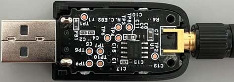
2ADLX-NC0110013M
Nov 13, 2023Network Controller
Equipment Class
JAD - Part 15 Class A Digital Device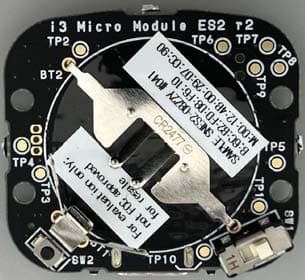
2ADLX-MM0110113M
Oct 29, 2023Sensor Module
Equipment Class
JAD - Part 15 Class A Digital Device