2AFCS-PGW10Low power device transmitter
SEQUANTA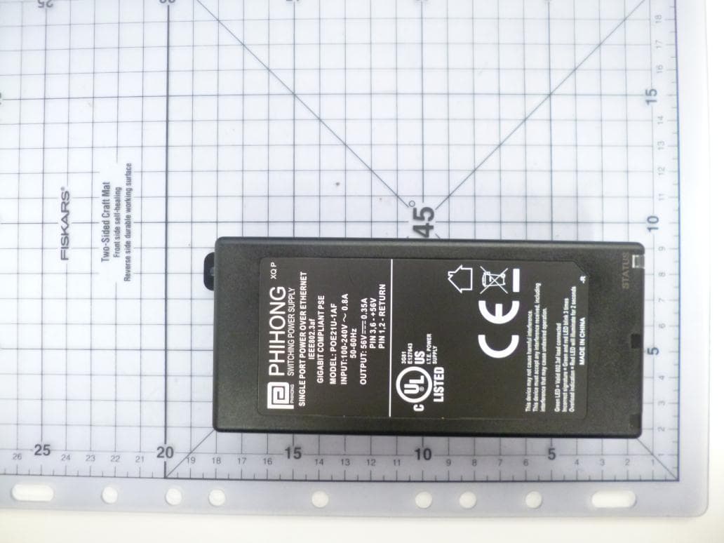
Click to zoom
Application Details
- Equipment Class
- DTS - Digital Transmission System
- Date of Grant
- Nov 10, 2015
- Application Purpose
- Original Equipment
- Date of Application
- Nov 10, 2015
- Equipment Note
- Low power device transmitter
- Frequency Range
- 2405.00000000 - 2475.00000000
- Company
- SEQUANTA
- Country
- France
Documents & Files
Document Text
Text extracted from the exhibit documents filed with the FCC. Open a document above to read the original.
Users Manual
HIKOB GATEWAY User Documentation Version 1.3-2466 This document may not be reproduced (even partially) or com- municated to 3rd parties without the written authorization of the company’s General Management. Copyright ©HIKOB. HIKOB GATEWAY Version 1.3-2466 October 2015·Page 2/ 15 Contents 1 Introduction3 1.1 Symbols and conventions used in this guide . . . . . . . . . . . . . . . . . . . . .3 1.2 Safety instructions . . . . . . . . . . . . . . . . . . . . . . . . . . . . . . . . . . .3 1.3 Compliance and conformity . . . . . . . . . . . . . . . . . . . . . . . . . . . . . .4 1.3.1Europe . . . . . . . . . . . . . . . . . . . . . . . . . . . . . . . . . . . .4 1.3.2Electromagnetic compatibility Japan . . . . . . . . . . . . . . . . . . . . .4 1.3.3USA . . . . . . . . . . . . . . . . . . . . . . . . . . . . . . . . . . . . . .4 1.3.4Canada . . . . . . . . . . . . . . . . . . . . . . . . . . . . . . . . . . . .5 1.4 WEEE . . . . . . . . . . . . . . . . . . . . . . . . . . . . . . . . . . . . . . . . . .5 1.5 Technical Support . . . . . . . . . . . . . . . . . . . . . . . . . . . . . . . . . . . .6 2 General description of the HIKOB GATEWAY7 2.1 HIKOB GATEWAY overview . . . . . . . . . . . . . . . . . . . . . . . . . . . . . .8 3 Data sheet9 4 Installation10 4.1 Overall methodology . . . . . . . . . . . . . . . . . . . . . . . . . . . . . . . . . . 10 4.2 Connection . . . . . . . . . . . . . . . . . . . . . . . . . . . . . . . . . . . . . . . 12 4.2.1PoE connection . . . . . . . . . . . . . . . . . . . . . . . . . . . . . . . . 12 4.2.2External antenna . . . . . . . . . . . . . . . . . . . . . . . . . . . . . . . 12 4.3 Outdoor deployment . . . . . . . . . . . . . . . . . . . . . . . . . . . . . . . . . . 13 4.3.1Ethernet cable set up for outdoor use . . . . . . . . . . . . . . . . . . . . 13 4.4 HIKOB GATEWAY Mounting procedure . . . . . . . . . . . . . . . . . . . . . . . . 14 HIKOB GATEWAY Version 1.3-2466 October 2015·Page 3/ 15 1 Introduction When using HIKOB GATEWAY, safety precautions must be taken to avoid injury and damages. Please read this guide before installing, using the product, or performing any maintenance operation. Failure to read, understand and follow herein instructions may result in personnal injury. In no event shall HIKOB be held liable for any damages arising out of or related to misunderstanding instructions detailed in this manual. 1.1 Symbols and conventions used in this guide Read entirely this guidebefore using the product HIKOB GATEWAY and keep it handy for reference. Caution– Indicates a potentially hazardous situation which, if instructions are not followed, may result in damage to the equipement. Electrical Hazard– Indicates a dangerous condition such that, if instruc- tions are not followed may result in electric shock and physical injury. – Carefully follow instructions and warnings given in this guide, as well as instructions indicated on the product. – Make sure you understand all instructions: refer to symbols definitions and conventions used in the documentation. – Should you have questions on using the product HIKOB GATEWAY once you have com- pletely read this guide, contact the HIKOB suppport or your vendor. 1.2 Safety instructions Do not disassemble or attempt to openthe product. It does not con- tain any serviceable parts inside. Only qualified staff is allowed to per- form maintenance operations on the HIKOB GATEWAY product. Opening a HIKOB GATEWAY will void the waranty. Do not overheat, do not dispose in fire, do not crush. Do not heat above 60°C, incinerate, or expose content to water: such improper use may lead to leakage, explosion or fire. Modifications or changes on the product is stricly prohibitedif it is not expressly approved by HIKOB. Modifications or changes performed on HIKOB GATEWAY will void the user’s authority to operate the equipment. HIKOB GATEWAY Version 1.3-2466 October 2015·Page 4/ 15 1.3 Compliance and conformity 1.3.1 Europe The HIKOB GATEWAY product is certified to be compliant with the R&TTE 1999/5/CE directive. Electromagnetic compatibility and radio spectrum The product HIKOB GATEWAY is certified to be compliant with the following standards: – ETSI EN 301 489-1 V1.9.2 (2011-09) et ETSI EN 301 489-17 V2.2.1 (2012-09) – ETSI EN 300 328 V1.8.1 et EN 62311 (2008) – ETSI EN 300 330-1 V1.7.1 (2010/02) et ETSI EN 300 330-2 V1.5.1 (2010/02) Electrical safety: The product HIKOB GATEWAY is certified to be compliant with the following normalized standards: – IEC 60950-1:2005 + A1:2010 + A2:2013 – EN 60950-1:2006 + A11:2009 + A1:2010 + A12:2011 + A2:2013 Models A and B of the HIKOB GATEWAY are certified to follow the EN CB 60 950-22 Am2 outdoor safety standard for electrical devices. With exception for Finland, Norway and Sweden, countries where environment temperature can be lower than operating and safety insurance temeratures for the HIKOB GATEWAY. You install the HIKOB GATEWAY indoors in those geographical areas. 1.3.2 Electromagnetic compatibility Japan The HIKOB GATEWAY product is certified to be compliant with Japan Radio Law - Article 2 paragraph 1 Item 19. 1.3.3 USA Information to userThis equipment has been tested and found to comply with the limits for a Class B digital device, pursuant to part 15 of the FCC Rules. These limits are designed to provide reasonable protection against harmful interference in a residential installation. This equipment generates, uses and can radiate radio frequency energy and, if not installed and used in accordance with the instruction, may cause harmful interference to radio communica- HIKOB GATEWAY Version 1.3-2466 October 2015·Page 5/ 15 tions. However, there is no guarantee that interference will not occur in a particular installation. If this equipment does cause harmful interference to radio or television reception which can be determined by turning the equipment off and on, the user is encouraged to try to correct interference by one or more of the following measures: – Reorient or rel…
Text truncated - open the document above for the full version.
Cover Letter(s)
Letter of Agency October 26, 2015 To: Federal Communications Commission 7435 Oakland Mills Road Columbia, MD 21046-1609 Curtis-Straus LLC TCB One Distribution Center Circle #1 Littleton, MA 01460 We, the undersigned HIKOB hereby authorize Anthony MERLIN, LCIE SUD EST, to act on our behalf in all matters relating to all processes required for FCC certification of our devices. Any and all acts carried out by the above agent on our behalf shall have the same effects as acts of our own. This authorization is valid until: December 1st, 2015 If you have any questions regarding this authorization, let us know please. Sincerely, Guillaume CHELIUS Signature
External Photos
Page 1/10 LCIE Laboratoire de Moirans Z.I. Centr’Alp 170, Rue de Chatagnon 38430 MOIRANS-FRANCE EXTERNAL PHOTOS OF EQUIPMENT FCCID: 2AFCS-PGW10 PGW1A and PGW1B Page 2/10 LCIE Laboratoire de Moirans Z.I. Centr’Alp 170, Rue de Chatagnon 38430 MOIRANS-FRANCE PGW1A and PGW1B Page 3/10 LCIE Laboratoire de Moirans Z.I. Centr’Alp 170, Rue de Chatagnon 38430 MOIRANS-FRANCE PGW1A and PGW1B Page 4/10 LCIE Laboratoire de Moirans Z.I. Centr’Alp 170, Rue de Chatagnon 38430 MOIRANS-FRANCE PGW1A and PGW1B Page 5/10 LCIE Laboratoire de Moirans Z.I. Centr’Alp 170, Rue de Chatagnon 38430 MOIRANS-FRANCE PGW1A and PGW1B Page 6/10 LCIE Laboratoire de Moirans Z.I. Centr’Alp 170, Rue de Chatagnon 38430 MOIRANS-FRANCE PGW1A and PGW1B Page 7/10 LCIE Laboratoire de Moirans Z.I. Centr’Alp 170, Rue de Chatagnon 38430 MOIRANS-FRANCE PGW1C (To show only difference with PGW1A and PGW1B) Page 8/10 LCIE Laboratoire de Moirans Z.I. Centr’Alp 170, Rue de Chatagnon 38430 MOIRANS-FRANCE Page 9/10 LCIE Laboratoire de Moirans Z.I. Centr’Alp 170, Rue de Chatagnon 38430 MOIRANS-FRANCE Page 10/10 LCIE Laboratoire de Moirans Z.I. Centr’Alp 170, Rue de Chatagnon 38430 MOIRANS-FRANCE
ID Label/Location Info
Page 1/4 LCIE Laboratoire de Moirans Z.I. Centr’Alp 170, Rue de Chatagnon 38430 MOIRANS-FRANCE PRODUCT LABELING FCCID: 2AFCS-PGW10 Page 2/4 LCIE Laboratoire de Moirans Z.I. Centr’Alp 170, Rue de Chatagnon 38430 MOIRANS-FRANCE Page 3/4 LCIE Laboratoire de Moirans Z.I. Centr’Alp 170, Rue de Chatagnon 38430 MOIRANS-FRANCE Page 4/4 LCIE Laboratoire de Moirans Z.I. Centr’Alp 170, Rue de Chatagnon 38430 MOIRANS-FRANCE
Internal Photos
Page 1/6 LCIE Laboratoire de Moirans Z.I. Centr’Alp 170, Rue de Chatagnon 38430 MOIRANS-FRANCE INTERNAL PHOTOS OF EQUIPMENT FCCID: 2AFCS-PGW10 PGW1C Page 2/6 LCIE Laboratoire de Moirans Z.I. Centr’Alp 170, Rue de Chatagnon 38430 MOIRANS-FRANCE PGW1A and PGW1B (Model “B” is without antenna only) Page 3/6 LCIE Laboratoire de Moirans Z.I. Centr’Alp 170, Rue de Chatagnon 38430 MOIRANS-FRANCE Page 4/6 LCIE Laboratoire de Moirans Z.I. Centr’Alp 170, Rue de Chatagnon 38430 MOIRANS-FRANCE Page 5/6 LCIE Laboratoire de Moirans Z.I. Centr’Alp 170, Rue de Chatagnon 38430 MOIRANS-FRANCE Page 6/6 LCIE Laboratoire de Moirans Z.I. Centr’Alp 170, Rue de Chatagnon 38430 MOIRANS-FRANCE
Operational Description
LCIE Laboratoire de Moirans Z.I. Centr’Alp 170, Rue de Chatagnon 38430 MOIRANS-FRANCE GENERAL INFORMATION FCCID: 2AFCS-PGW10 1.1. Product description LCIE Laboratoire de Moirans Z.I. Centr’Alp 170, Rue de Chatagnon 38430 MOIRANS-FRANCE LCIE Laboratoire de Moirans Z.I. Centr’Alp 170, Rue de Chatagnon 38430 MOIRANS-FRANCE 1.2. Tested System Details See test report 1.3. Test Methodology Both conducted and radiated testing were performed according to the procedures in ANSI C63.10 2013, FCC Part 15 Subpart C. Radiated testing was performed at an antenna to EUT distance of 10 meters. During testing, all equipment’s and cables were moved relative to each other in order to identify the worst case set-up. 1.4. Test facility Tests have been performed from May 5th to June 24th , 2015. This test facility has been fully described in a report and accepted by FCC as compliant with the radiated and AC line conducted test site criteria in ANSI C63.10 2013 (registration number 94821). This test facility has also been accredited by COFRAC (French accreditation authority for European Union test lab accreditation organization) according to NF EN ISO/IEC 17025, accreditation number 1-1633 as compliant with test site criteria and competence in 47 CFR Part 15/ANSI C63.4 and EN55022/CISPR22 norms for 89/336/EEC European EMC Directive application. All pertinent data for this test facility remains unchanged.
RF Exposure Info
LCIE Laboratoire de Moirans Z.I. Centr’Alp 170, Rue de Chatagnon 38430 MOIRANS-FRANCE FCCID: 2AFCS-PGW10 Prediction of MPE limit at a given distance Equation from page 18 of OET Bulletin 65, Edition 97-01 where:S = power density P = power input to the antenna G = power gain of the antenna in the direction of interest relative to an isotropic radiator R = distance to the center of radiation of the antenna Prediction Frequency MHz Conducted Output Power dBm Max Antenna Gain dBi Distance cm Power Density mW/cm2 Limit mW/cm2 2405 1.3 3200.00051.00 2440 1.2 3200.00051.00 2475 0.8 3200.00051.00 Conclusion: Therefore our device complies with FCC’s RF radiation exposure limits for general population without SAR evaluation with at least 20cm separation from all persons and must not be co-located or operating in conjunction with any other antenna or transmitter.
Test Report
This document shall not be reproduced, except in full, without the written approval of the LCIE. This document contains results related only to the item tested. It does not imply the conformity of the whole production to the item tested .Unless otherwise specified; the decision of conformity takes into account the uncertainty of measures. This document does not anticipate any certification decision. TEST REPORT N°: 832764-R2-E JDE : 135342 Subject Electromagnetic compatibility and Radio spectrum Matters (ERM) tests according to standards: FCC CFR 47 Part 15, Subpart B et C RSS-247 Ed 1.0 Issued to HIKOB 66 Boulevard Niels Bohr CS52132 69603 VILLEURBANNE CEDEX Product HIKOB GATEWAY Trade mark HIKOB Manufacturer HIKOB Model under test PGW1A / PGW1B / PGW1C Serial number BA:DB:0B:01:13/00:11:7B FCCID 2AFCS-PGW10 ICID 20474-PGW10 Test date From May 5 th to June 24 th , 2015 Test location Moirans IC Test site 6500A-1 & 6500A-3 Test performed by Jonathan PAUC / Jonathan SARTO Composition of document 40 pages Modification of the last version None Document issued on October 30th, 2015 Written by : Approved by : Jonathan PAUC Anthony MERLIN Tests operator Technical manager TEST REPORT N°832764-R2-E Page 2/40 SUMMARY 1. TEST PROGRAM ............................................................................................................................... 3 2. SYSTEM TEST CONFIGURATION ..................................................................................................... 4 3. CONDUCTED EMISSION DATA....................................................................................................... 10 4. RADIATED EMISSION DATA ........................................................................................................... 12 5. BANDWIDTH (15.247) ...................................................................................................................... 20 6. MAXIMUM PEAK OUTPUT POWER (15.247) .................................................................................. 23 7. POWER SPECTRAL DENSITY (15.247) .......................................................................................... 26 8. BAND EDGE MEASUREMENT (15.247) .......................................................................................... 28 9. OCCUPIED BANDWIDTH ................................................................................................................. 32 10. ANNEX 1 (GRAPHS) ........................................................................................................................ 34 11. UNCERTAINTIES CHART ................................................................................................................ 40 TEST REPORT N°832764-R2-E Page 3/40 1. TEST PROGRAM Standard: - FCC Part 15, Subpart C 15.247 - ANSI C63.4 (2014) / ANSI C63.10 (2013) - RSS-247 Issue 1.0 – May 2015 - RSS-Gen Issue 4 – Nov 2014 - 558074 D01 DTS Measurement Guidance v03r03 EMISSION TEST LIMITS RESULTS Limits for conducted disturbance at mains ports 150kHz-30MHz Frequency Quasi-peak value (dBμV) Average value (dBμV) PASS FAIL NA NP 150-500kHz 66 to 56 56 to 46 0.5-5MHz 56 46 5-30MHz 60 50 Radiated emissions 9kHz-30MHz CFR 47 §15.209 (a) CFR 47 §15.247 (d) RSS-247 §5.5 Measure at 300m 9kHz-490kHz : 67.6dBμV/m /F(kHz) Measure at 30m 490kHz-1.705MHz : 87.6dBμV/m /F(kHz) 1.705MHz-30MHz : 29.5 dBμV/m PASS FAIL NA NP Radiated emissions 30MHz-25GHz* CFR 47 §15.209 (a) CFR 47 §15.247 (d) RSS-247 §5.5 Highest frequency : 600MHz (Declaration of provider) Measure at 3m 30MHz-88MHz : 40 dBμV/m 88MHz-216MHz : 43.5 dBμV/m 216MHz-960MHz : 46.0 dBμV/m Above 960MHz : 54.0 dBμV/m PASS FAIL NA NP Bandwidth 6dB CFR 47 §15.247 (a) (2) RSS-247 §5.2.1 At least 500kHz PASS FAIL NA NP Power spectral Density CFR 47 §15.247 (e) RSS-247 §5.2.2 Limit: 8dBm/3kHz PASS FAIL NA NP Maximum Peak Output Power CFR 47 §15.247 (b) RSS-247 §5.4.4 Limit: 30dBm Conducted or Radiated measurement PASS FAIL NA NP Band Edge Measurement CFR 47 §15.209 (a) CFR 47 §15.247 (d) RSS-247 §5.5 Limit: -20dBc or Radiated emissions limits in restricted bands PASS FAIL NA NP Occupied bandwidth RSS-Gen §4.6.1 No limit PASS FAIL NA NP Receiver Spurious Emission** RSS-Gen §4.10 See RSS-Gen §4.10 PASS FAIL NA NP *§15.33: The highest internal source of a testing device is defined like more the highest frequency generated or used in the testing device or on which the testing device works or agrees. - If the highest frequency of the internal sources of the testing device is lower than 108 MHz, measurement must be only performed until 1GHz. - If the highest frequency of the internal sources of the testing device ranges between 108 MHz and 500 MHz, measurement must be only performed until 2GHz. - If the highest frequency of the internal sources of the testing device ranges between 500 MHz and 1 GHz, measurement must be only performed until 5GHz. If the highest frequency of the internal sources of the testing device is above 1 GHz, measurement must be only performed until 5 times the highest frequency or 40 GHz, while taking smallest of both. TEST REPORT N°832764-R2-E Page 4/40 2. SYSTEM TEST CONFIGURATION 2.1. JUSTIFICATION There are 3 models: PGW1A: 2.4GHz antenna internal and GPS, external used of equipment PGW1B: 2.4GHz antenna internal without GPS, external used of equipment PGW1C: 2.4GHz antenna external without GPS, internal used of equipment 2.2. HARDWARE IDENTIFICATION (EUT AND AUXILIARIES): Equipment under test (EUT): PGW1A / PGW1B / PGW1C Serial Number: BA:DB:0B:01:13/00:11:7B Equipment Under Test Power supply: During all the tests, EUT is supplied by V nom 240V/50Hz from PHIHONG For measurement with different voltage, it will be presented in test method. Name Type Rating Reference / Sn Comments Supply1 AC DC Battery Primary: 100-240V (50-60Hz) Secondary: 56Vdc (to Gateway PHIHONG Switching power supply POE21U…
Text truncated - open the document above for the full version.
Test Setup Photos
Page 1/5 LCIE Laboratoire de Moirans Z.I. Centr’Alp 170, Rue de Chatagnon 38430 MOIRANS-FRANCE CONDUCTED AND RADIATED MEASUREMENT PHOTO FCCID: 2AFCS-PGW10 1.1 Conducted emissions Page 2/5 LCIE Laboratoire de Moirans Z.I. Centr’Alp 170, Rue de Chatagnon 38430 MOIRANS-FRANCE 1.2 Radiated emissions XY Axis Z Axis Test setup in anechoic chamber Setup 15.247 & Subpart B (Configuration n°1) Page 3/5 LCIE Laboratoire de Moirans Z.I. Centr’Alp 170, Rue de Chatagnon 38430 MOIRANS-FRANCE XY Axis Z Axis Test setup in anechoic chamber Setup 15.247 (ZIGBEE)& Subpart B (Configuration n°2) Page 4/5 LCIE Laboratoire de Moirans Z.I. Centr’Alp 170, Rue de Chatagnon 38430 MOIRANS-FRANCE Above 1GHz setup Page 5/5 LCIE Laboratoire de Moirans Z.I. Centr’Alp 170, Rue de Chatagnon 38430 MOIRANS-FRANCE Test setup on OATS - §15.247 & §15.209 Configuration n°1 (Worst case)
Contact Information
Applicant
Thibault Martial
Test Firm
LCIE Etablissement Sud-EstAnthony Merlin
Technical Specifications
| # | Rule Parts | Frequency Range | Power Output |
|---|---|---|---|
| 1 | 15C | 2.40 GHz - 2.48 GHz | 1.35 mW |
Other Applications from SEQUANTA
2AFCS-PWC10
Dec 02, 2015Low power device transmitter
Equipment Class
DTS - Digital Transmission System
2AFCS-PAL20
Dec 02, 2015Low power device transmitter
Equipment Class
DTS - Digital Transmission System