2AFJR-DOWINBZ002DP LUMINOUS BUZZ SOCKET
DooGooD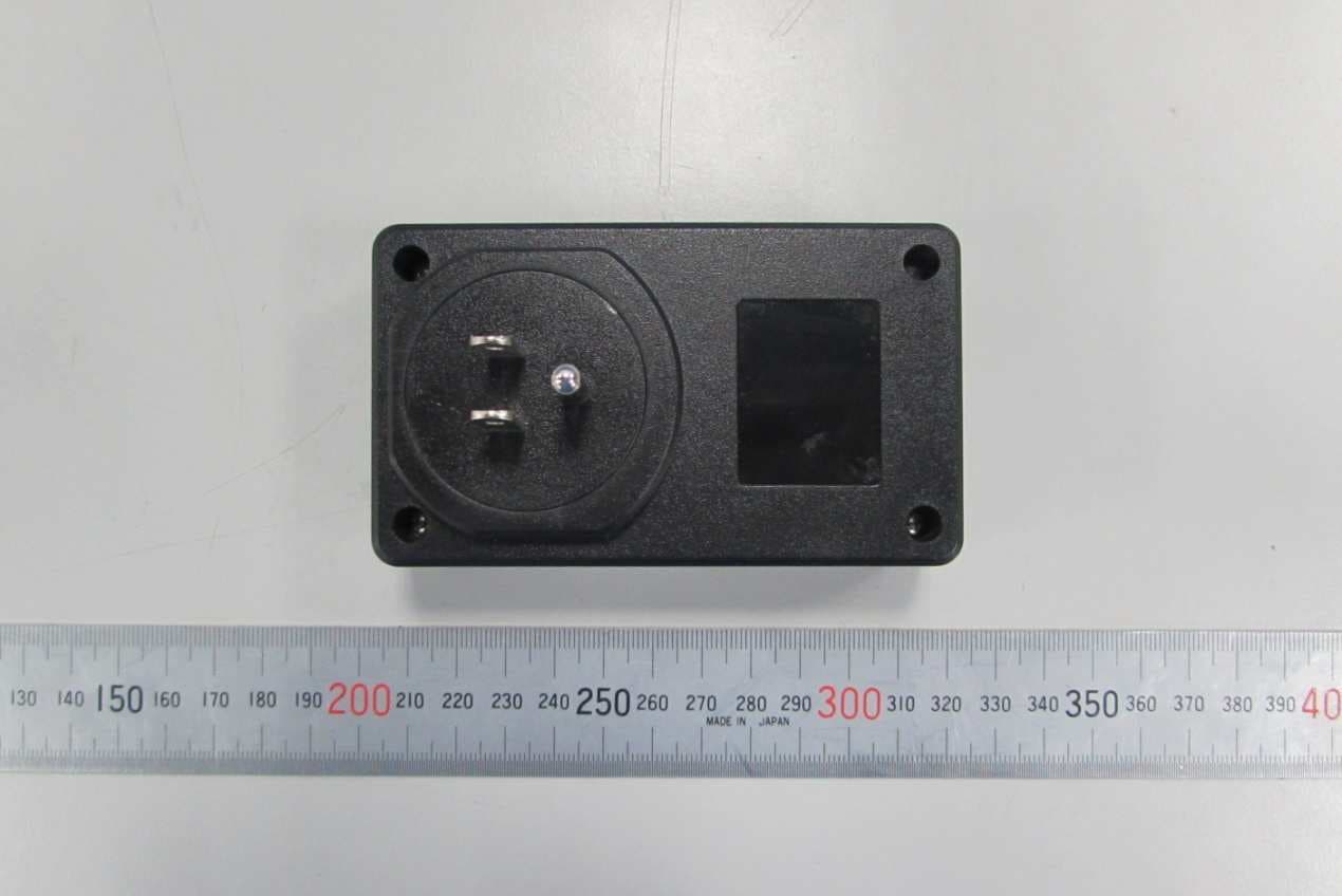
Click to zoom
Application Details
- Equipment Class
- CYY - Communications Receiver used w/Pt 15 Transmitter
- Date of Grant
- Sep 11, 2015
- Application Purpose
- Original Equipment
- Date of Application
- Sep 10, 2015
- Equipment Note
- DP LUMINOUS BUZZ SOCKET
- Frequency Range
- 433.92000000 - 433.92000000
- Company
- DooGooD
- Country
- France
Documents & Files
Document Text
Text extracted from the exhibit documents filed with the FCC. Open a document above to read the original.
Users Manual
DP LUMINOUS BUZZ (2034414) - Instruction for user 1 set: UK EU US LED charging indicator: Red: charging Green: fully charged Autonomy: 8 hours Char ging time: 6 hours Once you press on the shield, all items connected to the plugs lights up. WARNING: TECHNICAL DATA: - Not intended for use in play by children - Lithium battery - Please do not put in water - Life time: 500 charging - Do not store in a too hot or too humid place - CE agreement - Keep away from fire - Battery can’t be replaced RF radio distance: 30 meter Lighting Lighting Lighting LightingLightingLightingLightingLighting PUSH PUSH “GREEN/PINK/OFF” This device complies with Part 15 of the FCC Rules. Operation is subject to the following two conditions : (1) this device may not cause harmful interference. (2) this device must accept any interferencereceived, including interference that may cause undesired operation. Warning: Changes or modifications to this unit not expressly approved by the party responsible for compliance could void the user’s authority to operate the equipment. NOTE: This equipment has been tested and found to comply with the limits for a Class B digital device, pursuant to Part 15 of the FCC Rules. These limits are designed to provide reasonable protection against harmful interference in a residential installation. This equipment generates, uses and can radiate radio frequency energy and, if not installed and used in accordance with the instructions, may cause harmful interference to radio communications. However, there is no guarantee that interference will not occur in a particular installation. If this equipment does cause harmful interference to radio or television reception, which can be determined by turning the equipment off and on, the user is encouraged to try to correct the interference by one or more of the following measures: □ Reorient or relocate the receiving antenna. □ Increase the separation between the equipment and receiver. □ Connect the equipment into an outlet on a circuit different from that to which the receiver is connected. □ Consult the dealer or an experienced radio/TV technician for help.
Block Diagram
Block Diagram 模板 模板模板 模板 U3 218 Block Diagram U3 218 Block DiagramU3 218 Block Diagram U3 218 Block Diagram MCU SN 201 OSC:16MHZ POWRER LED INDICATOR U3 218R DC 5V AC:100-264V Oscillator=13.52127MHZ OUTPUT 433.92MHZ
Internal Photos
Internal view PCB view PCB View remove RF receiver module PCB Other side RF receiver module view
Operational Description
目 录 1.总体介绍.................................................................................... 1 2.产品特性: ............................................................................... 1 3.应用领域.................................................................................... 2 4.典型电路.................................................................................... 2 6. 引脚排布 ..................................................................................... 3 7.引脚描述.................................................................................... 3 8. 额定参数 ..................................................................................... 4 9. 工作参数 ..................................................................................... 4 10.功能描述 ................................................................................. 5 10.1 选择解调滤波器带宽 ...................................................................................................... 6 10.2 镜像抑制滤波器和带通滤波器 ...................................................................................... 6 10.3 自动增益控制(AGC)与C AGC 电容............................................................................ 6 10.4 参考振荡器与外部时钟 .................................................................................................. 7 10.5 SHUTDOWN功能 ........................................................................................................... 7 11. 典型应用 ................................................................................... 9 1 of 8 *This specification is subject to change without notification. 219R/218R 1.总体介绍 218R是法国OXO公司推出最新的单片300-450MHz无线ASK/OOK(ON-OFF Keyed) 接收芯片,主要应用于无线射频遥控领域。与上一代产品450R相比,218R不仅具有更高的 灵敏度(在433MHz应用环境下,灵敏度可以达到-109dBm),而且在芯片内部进一步集成 了镜像抑制功能,从而具有更强的抗干扰能力。这两点都使218R可以实现更远的接收距离。 同时,218R继承了450R “天线高频AM信号输入,数字信号输出”的特点,依然具有450R 同样的高集成度,高频信号接收功能全部集成于片内,以达到用最少的外围器件和最低的成 本获得最可靠的接收效果。同时,218R片内自动完成所有的RF及IF调谐,这样在开发和生 产中就省略了手工调节的工艺过程,自然也降低了成本,增强了产品的竞争力。 219R和218R均为16脚封装,219R为SSOP16, 218R为SOP16。 作为ASK/OOK 超外差接收器,SYN500R可以实现最大10Kbps的数据传输率,输入信 号的解调及滤波都集成在219R片内,用户可以在芯片外部选择四个带宽滤波器中的任何一 个,从而实现1.25KHz-10KHz的数据率。同时,用户还可以通过简单设置,来选择编码调 制格式和占空比。 2.产品特性: 完全的单片UHF接收器件 频率范围300—450 MHz 接收灵敏度-109dBm,1Kbps, 误码率10E-02 工作电压3V-5.5V 集成镜像抑制功能,数据率最大10Kbps 无需中频滤波器 低功耗: 6.0mA, 3.3V @ 433.92MHz 3.9mA, 3.3V @315MHz 2.5mA 2 of 8 *This specification is subject to change without notification. 219R/218R 0.9μA(关闭模式,shutdown mode) 250μA(315MHz,10: 1占空比) 带模拟RSSI输出 极佳的灵敏度和噪声抑制能力 标准的CMOS接口控制及解码数据输出 最经济的外围器件设计方案 3.应用领域 遥控键盘 远距离 RFID,RKE 遥控扇灯 遥控门 4.典型电路 433.92MHz 1K Baud Rate 3 of 8 *This specification is subject to change without notification. 219R/218R 315MHz 1K Baud Rate 6. 引脚排布 218R SOP16和219R SSOP16封装引脚图 7.引脚描述 引脚编号 引脚名 引脚功能 1 RO1 参考谐振器输入,连接Colpitts振荡器。或由外部参考信号驱动,最 大幅度1.5V峰峰值 2 GNDRF 负电源连接与天线RF输入 3 ANT 天线RF信号输入,内部AC耦合。建议使用带电感的匹配网络到RF 地,以增强ESD保护 4 GNDRF 负电源连接与天线RF输入 5 VDD 全芯片正电源输入 6 NC 未使用的引脚(浮空) 4 of 8 *This specification is subject to change without notification. 219R/218R 7 SEL0 逻辑控制输入,此引脚由内部上拉。与SEL1配合使用,控制解调低 通滤波器的带宽。 8 SHDN Shutdown逻辑控制输入,此引脚由内部上拉. 9 GND 全芯片负电源连接(除RF输入) 10 DO 解调数据输出 11 SEL1 逻辑控制输入,此引脚由内部上拉。与SEL0配合使用,控制解调低 通滤波器的带宽。 12 CTH 解调门限电压积分电容连接,获取调制波的平均值,用于内部数据 比较器的参考信号。使用外部电容连接CTH脚与地,建议使用1nF 以上电容,需根据数据率进行优化 13 CAGC AGC(Automatic Gain Control) 电容,推荐使用0.47uF或更大的电 容可以得到最好的效果。由该pin连接到地 14 RSSI 输出接收信号强度指示。由典型值为200 Ω阻抗的输出缓冲区输出 15 NC 未使用的引脚(接地) 16 RO2 参考谐振器输入,连接Colpitts振荡器。该引脚与地之间使用18pF 电容 8. 额定参数 电源电压(V DDRF , V DDBB ) +7V I/O端口电压 (V I/O ) V SS –0.3 to V DD +0.3 节点温度 (T J ) +150°C 储藏温度范围(T S ) –65°C to +150°C 焊接温度(焊接时间10秒) +260°C 9. 工作参数 射频频率范围 300MHz to 450MHz 电源电压 (VDD) +3.0V to +5.5V 最大输入RF功率 -20dBm 工作环境温度范围 (TA) –40°C to +85°C 防静电ESD灵敏度:符合1ESD级(2000V) 5 of 8 *This specification is subject to change without notification. 219R/218R 测试要求(手工模式,HBM),依据MIL-STD-883C标准,采用方法:Method 3015。 要求防静电储存,防静电操作 10.功能描述 如图所示:SYN500R分为四个功能块: UHF降频变换器 OOK解调器 参考时钟及控制 SHUTDOWN功能 用它组成一个完整的UHF接收器,只需要2个电容(C TH ,C AGC )和1个时钟器件(通 常为陶瓷振荡器),当然外部还需要1个电源滤波电容,3个输入控制脚(SEL0、SEL1、 SHDN)用来选择芯片的工作模式和带宽,芯片内部已有上拉电阻,不再需要外加上拉电阻。 6 of 8 *This specification is subject to change without notification. 219R/218R 10.1 选择解调滤波器带宽 SEL0、SEL1:选择解调滤波器带宽。用户应根据需要选择解调滤波器带宽: SEL0 SEL1 解调带宽 (@ 434MHz) 0 0 1625Hz 1 0 3250Hz 0 1 6500Hz 1 1 13000Hz-default 10.2 镜像抑制滤波器和带通滤波器 混频器的中频端口产生正交下变频中频信号,这些中频信号在通过镜像抑制滤波器以去 除镜像频率之前,先经过了低通滤波器,以去除较高的频率。之后中频信号通过一个三阶带 通滤波器,该滤波器中心频率1.2MHz,带宽是这330kHz @ 433.92MHz,带宽随RF工作频 率而变化,通过以下计算得出: BW IF = BW [email protected] MHz × Operating Freq(MHz) 433.92 以上滤波器全部集成于SYN500R之中。 10.3 自动增益控制(AGC)与C AGC 电容 自动增益控制(AGC)能增加输入动态范围。衰落与激励时间常数之比固定为10:1, 但激励时间常数能通过选择C AGC 的值来改变。 7 of 8 *This specification is subject to change without notification. 219R/218R 为了增大系统动态范围,在控制电平达到静态值时,应尽量减低AGC控制波纹(最好 低于10mv)。 10.4 参考振荡器与外部时钟 根据用户需要,可选择以下三种外部时钟: 陶瓷振荡器 晶体振荡器 外部时钟信号(如MCU输出时钟),幅度大约0.5V pp 用户应根据发射频率来确定时钟的值(详细如下): 上图中所有电容都已集成在SYN500R中,R01和R02的是外部引脚,用户只需要连接 参考振荡晶体。 参考振荡器晶体频率可以如下计算: F REF OSC = F RF /(32 + 1.1/12) 例如433.92 MHz, F REF OSC = 13.52127 MHz 10.5 SHUTDOWN功能 当SHDN脚输入高电平,芯片进入低功耗STANDBY模式,消耗电流小于1uA。 8 of 8 *This specification is subject to change without notification. 219R/218R 此脚内部被上拉,正常工作时必须下拉到地。 9 of 8 *This specification is subject to change without notification. 219R/218R 11. 典型应用 下图给出了433.92MHz频率下219R的典型应用
Operational Description
Circuit CircuitCircuit Circuit Description DescriptionDescription Description: :: : Part1: Power supply, transfer to DC12V and DC5V to the system power supply Part2:Receiving antenna, receiver the 433MHz and sent to the U3 Part3:Receiving module, disposing the signal, the type of receiver is super-heterodyne receiver Part4 : MCU control, receiver the signal from receiving mode and send the order to other part. Part5: LED indicator Part6:Control the load on the opening and closing of the load 13.52127MHz
Schematics
13.52127MHz
Test Report
Report No.: 150511029GZU-002 Issued: 2015-8-05 FCC ID: 2AFJR-DOWINBZ002 Page 1 of 17 TEST REPORT Applicant Name & Address : DooGooD 49 rue de Sèvres – 92100 BOULOGNE France Sample Description Product : DP LUMINOUS BUZZ SOCKET FCC ID 2AFJR-DOWINBZ002 Model No. : DW15U Electrical Rating : 125Vac/60Hz. Max power: 1875W. Date Received : 11 May 2015 Date Test Conducted : 11 May 2015 – 7 July 2015 Test standards : FCC Part 15: 2014 Subpart B Test Result : Pass Conclusion : The submitted samples complied with the above rules/standards. Remark : None. ***************************************End of Page*************************************** Prepared and Checked By: Approved By: _______________________ Signature Sky Zhu Helen Ma Engineer Team Leader Intertek Guangzhou Intertek Guangzhou 05 August 2015 Date This report is for the exclusive use of Intertek's Client and is provided pursuant to the agreement between Intertek and its Client. Intertek's responsibility and liability are limited to the terms and conditions of the agreement. Intertek assumes no liability to any party, other than to the Client in accordance with the agreement, for any loss, expense or damage occasioned by the use of this report. Only the Client is authorized to permit copying or distribution of this report and then only in its entirety. Any use of the Intertek name or one of its marks for the sale or advertisement of the tested material, product or service must first be approved in writing by Intertek. The observations and test results in this report are relevant only to the sample tested. This report by itself does not imply that the material, product, or service is or has ever been under an Intertek certification program. The test report only allows to be revised within three years from its original issued date unless further standard or the requirement was noticed. Intertek Testing Services Shenzhen Ltd. Guangzhou Branch Block E, No.7-2 Guang Dong Software Science Park, Caipin Road, Guangzhou Science City, GETDD Guangzhou, China Tel / Fax: 86-20-8213 9688/86-20-3205 7538 Report No.: 150511029GZU-002 Issued: 2015-8-05 FCC ID: 2AFJR-DOWINBZ002 Page 2 of 17 CONTENT TEST REPORT ....................................................................................................................................................................... 1 CONTENT ............................................................................................................................................................................... 2 1 TEST RESULTS SUMMARY ...................................................................................................................................... 3 2 TEST RESULTS CONCLUSION ................................................................................................................................ 4 3 LABORATORY MEASUREMENTS .......................................................................................................................... 5 4 TEST RESULTS ............................................................................................................................................................ 6 4.1 CONDUCTED DISTURBANCE VOLTAGE AT MAINS PORTS .............................................................................................. 6 4.1.1 Used Test Equipment ......................................................................................................................................... 6 4.1.2 Block Diagram of Test Setup ............................................................................................................................. 6 4.1.3 Test Setup and Procedure .................................................................................................................................. 6 4.1.4 Limit ................................................................................................................................................................... 7 4.1.5 Test Data and curve ........................................................................................................................................... 8 4.1.6 Measurement Uncertainty ................................................................................................................................. 9 4.2 RADIATED EMISSION (30 MHZ -1000 MHZ) ................................................................................................................ 9 4.2.1 Used Test Equipment ......................................................................................................................................... 9 4.2.2 Block Diagram of Test Setup ............................................................................................................................. 9 4.2.3 Test Setup and Procedure ................................................................................................................................ 10 4.2.4 Limit ................................................................................................................................................................. 10 4.2.5 Test Data.......................................................................................................................................................... 11 4.2.6 Test Curve ........................................................................................................................................................ 12 4.2.7 Measurement uncertainty ................................................................................................................................ 13 4.3 RADIATED EMISSION ABOVE 1 GHZ ........................................................................................................................... 13 4.3.1 Used Test Equipment ....................................................................................................................................... 13 4.3.2 Block Diagram…
Text truncated - open the document above for the full version.
Contact Information
Applicant
Fleur d'Avout
Technical Contact
Intertek Testing Services Shenzhen Ltd. GuangzhouSky Zhu
[email protected]86-20-82139691
Block E, No 7-2 Guang Dong Software Science Park · Guangzhou, Guangdong Provice · China
Test Firm
Intertek Testing Services Shenzhen Ltd.strong yao
[email protected]8628219940
Technical Specifications
| # | Rule Parts | Frequency Range | Power Output |
|---|---|---|---|
| 1 | 15B | 433.92 MHz - 433.92 MHz | - |
Other Applications from DooGooD

2AFJR-DOWINBZ001
Sep 11, 2015RF RADIO EMITTER FOR DP LUMINOUS BUZZ C1
Equipment Class
DSC - Part 15 Security/Remote Control Transmitter