2AFR8ED0991ED0991 UWB Module
InVue Security Products, Inc.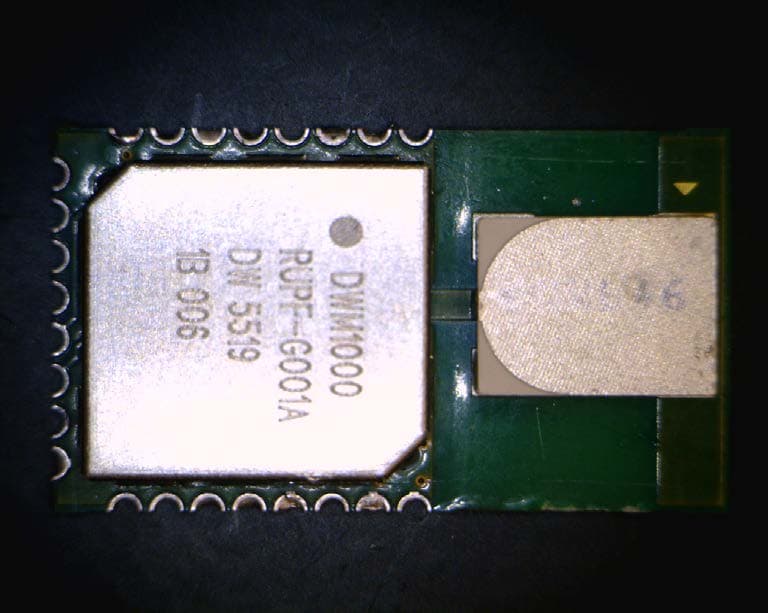
Click to zoom
Application Details
- Equipment Class
- UWB - Ultra Wideband Transmitter
- Date of Grant
- Nov 23, 2015
- Application Purpose
- Original Equipment
- Date of Application
- Oct 15, 2015
- Equipment Note
- ED0991 UWB Module
- Frequency Range
- 3659.15000000 - 4353.06000000
- Country
- United States
Documents & Files
Document Text
Text extracted from the exhibit documents filed with the FCC. Open a document above to read the original.
Users Manual
Model(s): ED0991 FCC ID: 2AFR8ED0991 ACS Project: 15-3027 Advanced Compliance Solutions Page 1 Certification Exhibit FCC ID: 2AFR8ED0991 FCC Rule Part: Part 15.517 ACS Project Number: 15-3027 Manufacturer: InVue Security Model: ED0991 Manual ED0991 Module, Users Manual Key Features The ED0991 is a modular transceiver to meet the requirements of 47 C.F.R. § 15.212 (i) The radio elements of the ED0991 have their own shielding. (ii) The ED0991 does not have modulation/data inputs. The modulation is generated internal and the modulation type is fixed as BPM w/ BPSK. The data rates are fixed and set to the module via an SPI interface to the host MCU. (iii) The modular transmitter has its own power supply regulator. An IEEE802.15.4-2011 UWB compliant wireless transceiver module based on DecaWave’s DW1000 IC. Fully coherent receiver for maximum range and accuracy. Designed to comply with FCC & ETSI UWB spectral masks Supply voltage 2.8V to 3.6V SPI Interface to host processor Key Benefits High immunity to multipath fading – allows reliable communications in high fading environments Low power consumption allows operation from batteries for long periods* Small physical size allows the implementation of cost-effective solutions in RTLS and WSN Integrated antenna allows simple product implementation – no RF design required Integration of DW1000 IC, antenna, power management and clock control simplifies design integration Very precise location of tagged objects delivers enterprise efficiency gains and cost reductions Long LOS and NLOS range reduces amount of infrastructure required to deploy systems Low power consumption reduces the need to replace batteries and lowers system lifetime costs Standards based solution (IEEE802.15.4-2011), eases proliferation Low cost allows cost-effective implementation of solutions The ED0991 module interfaces to an application microcontroller via SPI bus. Physical and MAC layer functionality are accessed via the SPI bus, through addressable registers as well as execution commands. Data received or to be transmitted are also accessed through the SPI bus and are implemented as a FIFO register (64 bytes each for TX and RX). To transmit, a frame of data is placed in the FIFO, this may include a destination address. A transmit command is given, which will transmit the data according to the initial setup of the registers. To receive data a receive command is given, which will listen for a transmission and when one occurs put the received frame in the FIFO. When neither transmit nor receive is required the device can enter either an Idle mode, from which it can quickly re-enter receive or transmit mode or it can enter a low power sleep mode, from which a crystal startup is also required prior to transmit or receive operation. A block diagram is given for the ED0991 module in Figure 1. Antenna The antenna couples energy between the air and the module. The ED0991 module has an integrated antenna that is near omni-directional. Note that the end radiation pattern depend not only on the antenna, but also the ground plane, enclosure and installation environment. Matching The matching provides the correct loading of the transmit amplifier to achieve the highest output power as well as the correct loading for the receive LNA to achieve the best sensitivity. Physical The physical layer provides conversions between data, symbol and RF signal. MAC The MAC layer is part of the Logical Link Layer and provides frame handling, addressing and medium access services. Microcontroller Interface The microcontroller interface exposes registers and commands for the physical and MAC layers to a microcontroller. Power Management Power management ensures a stable supply for the internal functions as well as providing means for a low power sleep mode, in which most of the transceiver is power off. Figure 1 Typical Flow After initial setup of registers for desired behavior, the normal operation flow diagram is shown in. In applications of infrequent data transmissions the transceiver would be in SLEEP mode to save power (<100nA). From there it would be woken up and enter WAKEUP mode. As part of the wake up process the crystal oscillator is started (~4ms) and the digital microcontroller interface is powered up. Before transmit or receive the frequency synthesizer needs to be started RSTn and having been powered off (or idle for a while) the control loop of the VCO/PLL needs to be calibrated INIT. A data frame is loaded into the transmit FIFO and the TX mode is entered. In the TX state the DW1000 actively transmits a frame containing the contents of the transmit buffer on the configured RF channel with the configured transmit parameters (PRF, data rate, preamble code etc.) Once the frame transmission is complete the DW1000 may enter one of three modes depending on the programmed configuration. After the frame transmission is complete the DW1000 will return to the IDLE state unless the ATXSLP bit is set (in Sub-Register 0x36:04 – PMSC_CTRL1) in which case the DW1000 will enter the SLEEP or DEEPSLEEP state automatically, (as long as no host interrupts are pending). When transmit is complete RX mode is entered to either hunting for preamble or (once it has detected preamble) actively receiving preamble searching for SFD, and subsequently receiving the PHR, decoding it and receiving the data part of the frame. In the RX state, the RF synthesizer and all RX blocks are active. After an event that ends the reception, (either a good frame RX, or some error or timeout event that aborts reception) the DW1000 will return to the IDLE state unless the ARXSLP bit is set (in Sub-Register 0x36:04 – PMSC_CTRL1) in which case the DW1000 will enter the SLEEP or DEEPSLEEP state automatically (as long as no host interrupts are pending). Contents Key Features ...................................................................................................................…
Text truncated - open the document above for the full version.
Cover Letter(s)
5015 B. U. Bowman Dr. Buford, GA 30518 September 22, 2015 ACS TCB 5015 B.U. Bowman Drive Buford, GA 30518 Re: FCC ID: 2AFR8ED0991 To Whom It May Concern: The following application is submitted on behalf of our client, InVue Security Products, for evaluation of their model ED0991 for certification under FCC Part 15 Subpart F for limited modular approval. The ED0991 module is a self contained RF circuit consisting of the UWB transceiver system and antenna in a chip like package 0.875 X 0.5 inches. The ED0991 was tested in full to the requirements of the aforementioned rules and was found to be in compliance. Sincerely, Sam Wismer Vice President, Technology Advanced Compliance Solutions, Inc.
External Photos
2320 Presidential Drive, Suite 101, Durham, NC 27703 USA Voice: 919-381-4235 Certification Exhibit FCC ID: 2AFR8ED0991 FCC Rule Part: Part 15.517 ACS Project Number: 15-3027 Manufacturer: InVue Security Model: ED0991 External Photos Model(s): ED0991 FCC ID: 2AFR8ED0991 ACS Project: 15-3027 Advanced Compliance Solutions Page 2 Figure 1: PCB - Front Figure 3: PCB - Back
ID Label/Location Info
Model(s): ED0991 FCC ID: 2AFR8ED0991 ACS Project: 15-3027 Advanced Compliance Solutions Page 1 Certification Exhibit FCC ID: 2AFR8ED0991 FCC Rule Part: Part 15.517 ACS Project Number: 15-3027 Manufacturer: InVue Security Model: ED0991 Label 2 0.50 0.35 0.25 0.15 0.10 ANGLES 150 < L 65 < L ≤ 150 20 < L ≤ 65 5 < L ≤ 20 L ≤ 5 TOLERANCE TOLERANCE TABLE (MM) UNLESS OTHERWISE SPECIFIED DIMENSION 2 6 4 5 1 3 8 7 9 2 2 Place label F1443018 as shown 2 Notes: Soldering must be performed within the guidelines of IPC-J-STD-001E or any revision that supersedes said standard.1. Soldered assemblies must be cleaned within the guidelines of IPC-CH-65B or any revision that supersedes said standard.2. Finished PCBA must comply with IPC-A-610E CLASS 2 requirements or any revision that supersedes said standard3. Wiring and cabling workmanship must comply with IPC/WHMA-A-620A CLASS 2 requirements or any revision that supersedes said standard.4. Assembly must comply with ROHS directives.5. F1443201 and F1443601 are connected by a header and soldered.6. F1443201 and F1443301/F1443311/F1443321 are connected by a header and soldered.7. F1443501 is connected to F1443201 by QTY-2 28AWG, 41 strand wires. Wire length should be sized appropriately for assembly in F1443102.8. C40021 and ED0330 are soldered to F1443201.9. C70226 is crimped to F1443140 according to the dimensions above and then soldered to F1443201.10. Add glue to all PCBA wire solder points to increase durability/reliability.11. 1 1 REVISIONS REVDESCRIPTIONRELEASEDCHECKEDDATE 0InitialKMBRPG9-DEC-2014 1Added E5 call out, updated notesKMB8/25/2015 2Added FCC labelKMB10/12/2015 ITEM NO.PART NUMBERDESCRIPTIONF1443200-01BF1443200-01WF1443200-02BF1443200-02WF1443200-03BF1443200-03W 1C40021Piezo111111 2ED0330BATTERY LI-PO 3.7V 180mAh111111 3F1443501Base Plunger PCBA111111 4F1443201Base Center PCBA111111 5F1443601Base Front PCBA111111 6F1443321Base Top PCBA - Red LED----11 6F1443301Base Top PCBA - Gold LED11---- 6F1443311Base Top PCBA - Blue LED--11-- 7F1443140-BUSB 2.0 Power Cable Assembly - Black1-1-1- 7F1443140-WUSB 2.0 Power Cable Assembly, White-1-1-1 8C70226 Ear clamp (Oetiker P/N 10100002 or appvd equiv) 111111 9F1443018UWB Module FCC Label111111 F1443201 DESIGNATOR F1443501 DESIGNATOR P8E1, 28AWG White P9E2, 28AWG Black F1443201 DESIGNATOR Battery Bat +Red Bat -Black F1443201 DESIGNATOR Piezo P5Red P6Black F1443201 DESIGNATOR USB-A Cable E1Red E2White E3Green E4Black E5Shield Wire DRAWING NO. F1443200 SHEET 1 OF 1 REV F1443200 2 ABCDEFGHIJKL 1 2 3 4 5 6 7 8 ACEGIKBDFHJL 7 1 4 6 8 2 5 3 F1443 KMB PROJECT NO.ENGINEER MASS (GRAMS) 17.12 Wireless AP InVue Security Products 15015 Lancaster Hwy Charlotte, NC 28277 Phone: 704-752-6513 e-FAX: 704-943-1528 TITLE MM DRAWING NO. UNITS THIS DRAWING IS PROPERTY OF INVUE SECURITY PRODUCTS, INC. AND IS LOANED UPON CONDITION THAT IT IS NOT TO BE REPRODUCED OR COPIED IN WHOLE OR IN PART, OR USED FOR FURNISHING INFORMATION TO OTHERS, OR FOR ANY OTHER PURPOSE DETRIMENTAL TO THE INTEREST OF INVUE SECURITY PRODUCTS, INC. AND WILL BE RETURNED UPON REQUEST PROPRIETARY AND CONFIDENTIAL SHEET 1 OF 1 Base PCBA Sub-Assembly 2 0.50 0.35 0.25 0.15 0.10 ANGLES 150 < L 65 < L ≤ 150 20 < L ≤ 65 5 < L ≤ 20 L ≤ 5 TOLERANCE TOLERANCE TABLE (MM) UNLESS OTHERWISE SPECIFIED DIMENSION 2 3 1 4 2 Place label F1443018 as shown Notes: Soldering must be performed within the guidelines of IPC-J-STD-001E or any revision that supersedes said standard.1. Soldered assemblies must be cleaned within the guidelines of IPC-CH-65B or any revision that supersedes said standard.2. Finished PCBA must comply with IPC-A-610E CLASS 2 requirements or any revision that supersedes said standard3. Wiring and cabling workmanship must comply with IPC/WHMA-A-620A CLASS 2 requirements or any revision that supersedes said standard.4. Assembly must comply with ROHS directives.5. ED0652 is soldered to F14434xx and then adhered to F14434xx within the pad printed outline using C70227.6. 1 1 2 REVISIONS REVDESCRIPTIONRELEASEDCHECKEDDATE 0InitialKMBRPG5-DEC-2014 1Updated BOMKMBRPG1/26/2015 2Added FCC LogoKMB10/12/2015 ITEM NO. PART NUMBER DESCRIPTIONF1443400-01F1443400-02F1443400-03F1443400-04 1F1443431Sensor PCBA - Lightning - Blue LED---1 1F1443401Sensor PCBA - Micro-USB - Yellow or Red LED1--- 1F1443411Sensor PCBA - Micro-USB - Blue LED-1-- 1F1443421Sensor PCBA - Lightning - Yellow or Red LED--1- 2ED0652Battery, Lipo, 3.7V, 65mAh1111 3C702273M 4032 Adhesive, 1/4" x 1/2"1111 4F1443018UWB Module FCC Label1111 F14434xx Designator Battery Wire Color B+Red B-Black DRAWING NO. F1443400 SHEET 1 OF 1 REV F1443400 2 ABCDEFGHIJKL 1 2 3 4 5 6 7 8 ACEGIKBDFHJL 7 1 4 6 8 2 5 3 F1443 KMB PROJECT NO.ENGINEER MASS (GRAMS) 21.81 Wireless AP InVue Security Products 15015 Lancaster Hwy Charlotte, NC 28277 Phone: 704-752-6513 e-FAX: 704-943-1528 TITLE MM DRAWING NO. UNITS THIS DRAWING IS PROPERTY OF INVUE SECURITY PRODUCTS, INC. AND IS LOANED UPON CONDITION THAT IT IS NOT TO BE REPRODUCED OR COPIED IN WHOLE OR IN PART, OR USED FOR FURNISHING INFORMATION TO OTHERS, OR FOR ANY OTHER PURPOSE DETRIMENTAL TO THE INTEREST OF INVUE SECURITY PRODUCTS, INC. AND WILL BE RETURNED UPON REQUEST PROPRIETARY AND CONFIDENTIAL SHEET 1 OF 1 Sensor PCBA ASM 2 0.50 0.35 0.25 0.15 0.10 ANGLES 150 < L 65 < L ≤ 150 20 < L ≤ 65 5 < L ≤ 20 L ≤ 5 TOLERANCE TOLERANCE TABLE (MM) UNLESS OTHERWISE SPECIFIED DIMENSION 4.00 10.00 Text as shown. Font: Helvetica LT, 4pt Adhesive side NOTES: Material: Polycarbonate1. Acrylic adhesive on one side only.2. REVISIONS REVDESCRIPTIONRELEASEDCHECKEDDATE 0InitialKMB12-Oct-2015 DRAWING NO. F1443018 SHEET 1 OF 1 REV F1443018 0 ABCDEFGHIJKL 1 2 3 4 5 6 7 8 ACEGIKBDFHJL 7 1 4 6 8 2 5 3 F1443 KMB PROJECT NO.ENGINEER MASS (GRAMS) 0.00 Wireless AP InVue Security Products 15015 Lancaster Hwy Charlotte, NC 28277 Phone: 704-752-6513 e-FAX: 704-943-1528 TITLE MM DRAWING NO. UNITS THIS DRAWING IS PROPERTY OF INVUE SECURITY PRODUCTS, INC. AND IS LOANED UPON CONDITION THAT IT IS NOT TO BE REPRODUCED…
Text truncated - open the document above for the full version.
Internal Photos
2320 Presidential Drive, Suite 101, Durham, NC 27703 USA Voice: 919-381-4235 Certification Exhibit FCC ID: 2AFR8ED0991 FCC Rule Part: Part 15.517 ACS Project Number: 15-3027 Manufacturer: InVue Security Model: ED0991 Internal Photos Model(s): ED0991 FCC ID: 2AFR8ED0991 ACS Project: 15-3027 Advanced Compliance Solutions Page 2 Figure 1: PCB with Shield - Front Figure 2: PCB without Shield - Front Model(s): ED0991 FCC ID: 2AFR8ED0991 ACS Project: 15-3027 Advanced Compliance Solutions Page 3 Figure 3: PCB - Back
Test Report
2320 Presidential Dr Suite 101, Durham NC 27703-8077, Ph: 919-381-4235 Certification Test Report FCC ID: 2AFR8ED0991 FCC Rule Part: Part 15.517 ACS Report Number: 15-3027.W03.1A Manufacturer: InVue Security Model: ED0991 Test Begin Date: July 7, 2015 Test End Date: July 28, 2015 Report Issue Date: October 14, 2015 FOR THE SCOPE OF ACCREDITATION UNDER LAB Code AT-1921 This report must not be used by the client to claim product certification, approval, or endorsement by ANAB, ANSI, or any agency of the Federal Government. Reviewed by: Mario de Aranzeta Lab Manager Durham (RTP) ACS Inc. This test report shall not be reproduced except in full. This report may be reproduced in part with prior written consent of ACS, Inc. The results contained in this report are representative of the sample(s) submitted for evaluation. This report contains 21 pages 2320 Presidential Drive Suite 101 Durham NC 27703-8077 USA, PH: 919-4381-4235 TABLE OF CONTENTS 1 GENERAL ............................................................................................................................................ 3 1.1 PURPOSE .......................................................................................................................................... 3 1.2 PRODUCT DESCRIPTION ...................................................................................................................... 3 1.3 TEST METHODOLOGY AND CONSIDERATIONS....................................................................................... 4 1.4 LOCATION ............................................................................................................................................. 4 1.5 LABORATORY ACCREDITATIONS/RECOGNITIONS/CERTIFICATIONS ...................................................... 4 1.6 RADIATED EMISSIONS TEST SITE DESCRIPTION .................................................................................... 5 1.6.1 Semi-Anechoic Chamber Test Site ................................................................................................ 5 1.7 CONDUCTED EMISSIONS TEST SITE DESCRIPTION ................................................................................ 6 2 APPLICABLE STANDARD REFERENCES .................................................................................... 6 3 LIST OF TEST EQUIPMENT ............................................................................................................ 7 4 SUPPORT EQUIPMENT .................................................................................................................... 8 5 EQUIPMENT UNDER TEST SETUP BLOCK DIAGRAM ........................................................... 9 6 SUMMARY OF TESTS ......................................................................................................................10 6.1 ANTENNA REQUIREMENT – FCC 15.203..............................................................................................10 6.2 POWER LINE CONDUCTED EMISSIONS – FCC 15.207...........................................................................10 6.2.1 Measurement Procedure ..............................................................................................................10 6.2.2 Measurement Results ...................................................................................................................10 6.3 10 DB BANDWIDTH – FCC 15.517(B) ..................................................................................................11 6.3.1 Measurement Procedure ..............................................................................................................11 6.3.2 Measurement Results ...................................................................................................................11 6.4 FUNDAMENTAL EMISSION PEAK POWER – FCC 15.517(E) ..................................................................12 6.4.1 Measurement Procedure ..............................................................................................................12 6.4.2 Measurement Results ...................................................................................................................12 6.5 POWER SPECTRAL DENSITY IN THE FUNDAMENTAL EMISSION – FCC 15.517(C). ...............................13 6.5.1 Measurement Procedure ..............................................................................................................13 6.5.2 Measurement Results ...................................................................................................................13 6.6 RADIATED EMISSIONS – FCC 15.517(C), 15.209 ................................................................................14 6.6.1 Emissions into Frequency Bands above 960 MHz .......................................................................14 6.6.1.1 MEASUREMENT PROCEDURE .........................................................................................................14 6.6.1.2 SAMPLE CALCULATION: ................................................................................................................14 6.6.1.3 MEASUREMENT RESULTS ..............................................................................................................14 6.6.2 Emissions into Frequency Bands below 960 MHz .......................................................................19 6.6.2.1 MEASUREMENT PROCEDURE .........................................................................................................19 6.6.2.2 MEASUREMENT RESULTS ..............................................................................................................19 6.6.3 Radiated Emissions in the GPS bands FCC 15.517(d) ................................................................20 6.6.3.1 MEASUREMENT PROCEDURE .........................................................................................................20 6.6.3.2 MEASUREMENT RESULTS: ..........................…
Text truncated - open the document above for the full version.
Test Setup Photos
2320 Presidential Drive, Suite 101, Durham, NC 27703 USA Voice: 919-381-4235 Certification Exhibit FCC ID: 2AFR8ED0991 FCC Rule Part: Part 15.517 ACS Project Number: 15-3027 Manufacturer: InVue Security Model: ED0991 Test Setup Photos Model(s): ED0991 FCC ID: 2AFR8ED0991 ACS Project: 15-3027 Advanced Compliance Solutions Page 2 Figure 1: Antenna Horizontal Figure 2: Antenna Vertical Model(s): ED0991 FCC ID: 2AFR8ED0991 ACS Project: 15-3027 Advanced Compliance Solutions Page 3 Figure 3: Flat Figure 4: Radiated Emissions – Above 1GHz Model(s): ED0991 FCC ID: 2AFR8ED0991 ACS Project: 15-3027 Advanced Compliance Solutions Page 4 Figure 5: Radiated Emissions – Below 1GHz Figure 6: Power Line Conducted – Front View Model(s): ED0991 FCC ID: 2AFR8ED0991 ACS Project: 15-3027 Advanced Compliance Solutions Page 5 Figure 7: Power Line Conducted – Side View
Contact Information
Applicant
Rob Spadafore(Compliance Engineer)
Test Firm
TUV SUD America, Inc.Sam Wismer
Technical Specifications
| # | Rule Parts | Frequency Range | Power Output |
|---|---|---|---|
| 1 | 15F | 3.66 GHz - 4.35 GHz | 1.00 mW |
Other Applications from InVue Security Products, Inc.
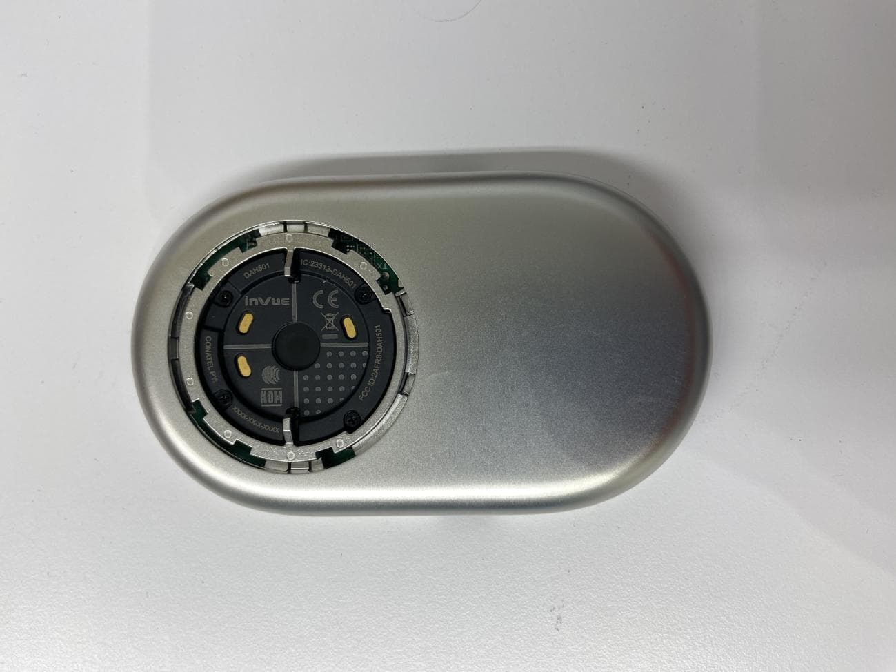
2AFR8-DAH501
Jul 16, 2026Retail Phone and Tablet Security Display Stand Charger
Equipment Class
DCD - Part 15 Low Power Transmitter Below 1705 kHz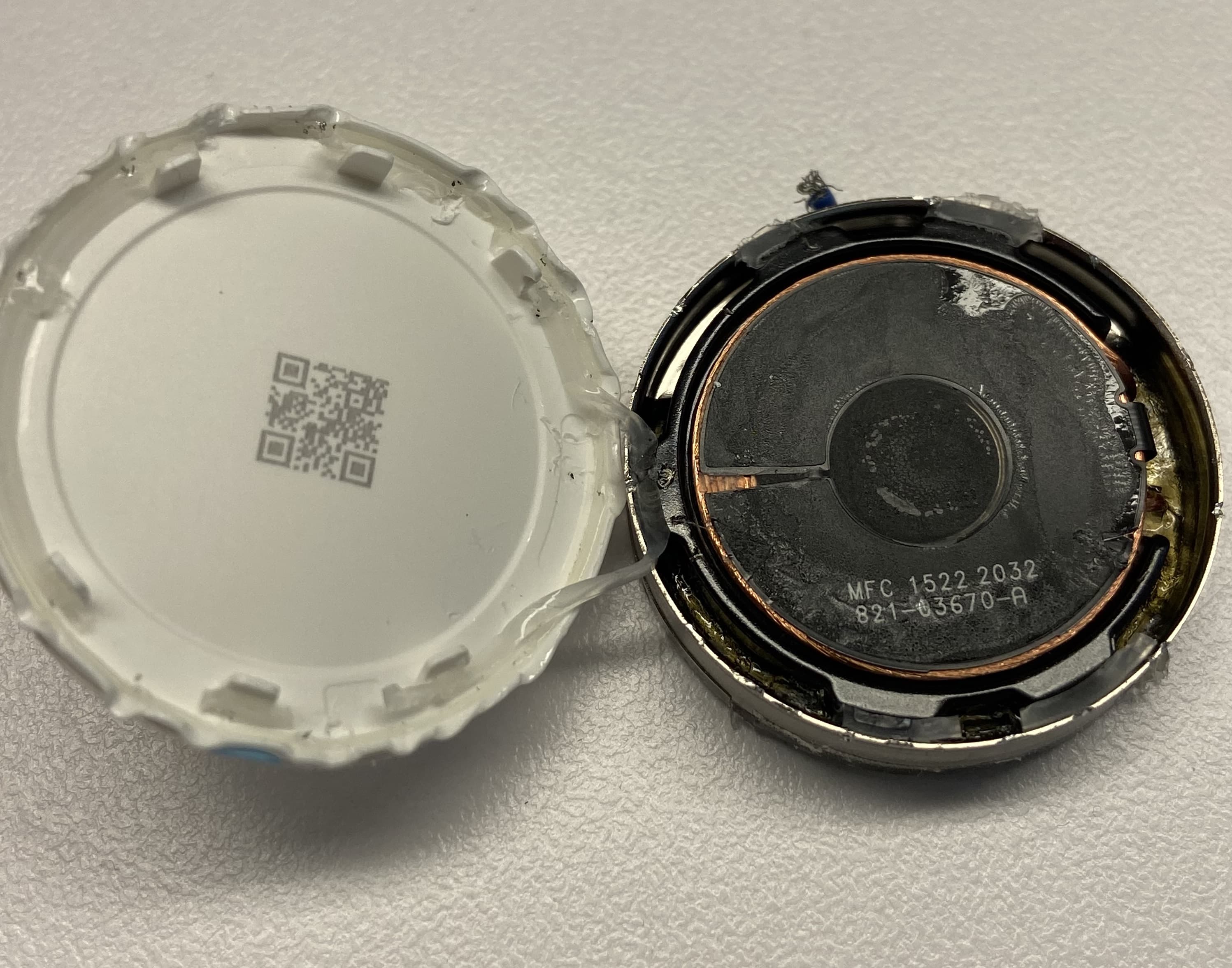
2AFR8-P05BRLT
Mar 31, 2024Watch Sensor Bracelet
Equipment Class
DXX - Part 15 Low Power Communication Device Transmitter