2AG94-F6988bluetooth module
Shenzhenshi Xinzhongxin Technology Co., Ltd.
Click to zoom
Application Details
- Equipment Class
- DSS - Part 15 Spread Spectrum Transmitter
- Date of Grant
- Apr 05, 2022
- Application Purpose
- Original Equipment
- Date of Application
- Apr 05, 2022
- Equipment Note
- bluetooth module
- Frequency Range
- 2402.00000000 - 2480.00000000
- Country
- China
Documents & Files
Document Text
Text extracted from the exhibit documents filed with the FCC. Open a document above to read the original.
Users Manual
SHENZHENSHI XINZHONGXIN TECHNOLOGY CO., LTD. ADDRESS:Block 3,Dong Huan Industrial Park,Sha Jing Town,Bao’an District,Shenzhen City,Guangdong, China TEL:0755-29179480/81 /82 FAX: 0755-84736169 W EB:WWW.C-CHIP.COM.CN F-6988 Specification Product name:Bluetooth module Product model:F-6988 Document No:XZX-SPEC-BT-RD-023 Document Version:V2.5 Availability Date:2018-06-25 File include(C-CHIP) fonfidential documents,without permission,can not be disclosed Edit Review Approve SHENZHENSHI XINZHONGXIN TECHNOLOGY CO., LTD. ADDRESS:Block 3,Dong Huan Industrial Park,Sha Jing Town,Bao’an District,Shenzhen City, Guangdong, China TEL:0755-29179480/81 /82 FAX: 0755-84736169 W EB:WWW.C-CHIP.COM.CN F-6988 变更履历 Version Change Information Page Date Editor V2.0 Initial issue / 2018-03-06 WuDeLong V2.1 GPIO_5 is in tune with GPIO_15 / 2018-03-20 WuDeLong V2.2 GPIO_10 is in tune with GPIO_14 GPIO_5 is in tune with GPIO_9 2018-04-08 WuDeLong V2.3 Increase: Module packaging material height dimensions. 2018-04-24 WuDeLong V2.4 The 40th pin of the module is changed from GND to agnd 2018-05-24 Xiesansh un V2.5 Bluetooth version upgraded from 4.2 to 5.0 2018-06-25 Liuxiong chao Content SHENZHENSHI XINZHONGXIN TECHNOLOGY CO., LTD. ADDRESS:Block 3,Dong Huan Industrial Park,Sha Jing Town,Bao’an District,Shenzhen City, Guangdong, China TEL:0755-29179480/81 /82 FAX: 0755-84736169 W EB:WWW.C-CHIP.COM.CN F-6988 一、Product overview: ............................................................................................................................................... 4 二、Application area: ................................................................................................................................................. 4 三、Features: .............................................................................................................................................................. 4 四、performance parameter: ..................................................................................................................................... 5 五、Module block diagram: ....................................................................................................................................... 6 六、The size of the module graph: ............................................................................................................................ 7 七、Module packaging material height dimensions: ................................................................................................... 8 八、Device pin out diagrm : ...................................................................................................................................... 9 九、Pin definition : .................................................................................................................................................... 9 十、Design notes: ..................................................................................................................................................... 11 十一、N o t e s: .......................................................................................................................................................... 11 十二、Recommended reflow temperature: ............................................................................................................ 12 十三、Application schematic diagram: ................................................................................................................... 12 SHENZHENSHI XINZHONGXIN TECHNOLOGY CO., LTD. ADDRESS:Block 3,Dong Huan Industrial Park,Sha Jing Town,Bao’an District,Shenzhen City, Guangdong, China TEL:0755-29179480/81 /82 FAX: 0755-84736169 W EB:WWW.C-CHIP.COM.CN F-6988 一、Product overview: F - 6 9 8 8 i s t h e B l u e t o o t h m o d u l e f o r i n t e l l i g e n t w i r e l e s s a u d i o t r a n s m i s s i o n p r o d u c t s d e s i g n e d b y o u r c o m p a n y . F- 6 9 8 8 a l s o i s t h e l o w c o s t s t e r e o a u d i o B l u e t o o t h s o l u t i o n w i t h h i g h p e r f o r m a n c e . T h e m a i n c h i p u s e s B E K E N B K 3 2 6 6 c h i p Q F N 4 0 p a c k a g i n g d e s i g n . W i t h o u t a n y d r i v e r, y o u c a n c o n n e c t t h e m o d u l e w i t h y o u r d e v i c e t o e n j o y t h e h i g h q u a l i t y m u s i c e a s i l y a n d s i m p l e d a t a t r a n s m i s s i o n f u n c t i o n s . I t s u p p o r t s i n t e l l i g e n t v o i c e p r o m p t i n g a n d r e p o r t i n g n u m b e r f u n c t i o n , i n t e g r a t e d T F c a r d p l a y b a c k f u n c t i o n a n d i n t e g r a t e d m o bi l e U S B- d i s k p l a y b a c k f u n c t i o n . I t a l s o s u p p o r t s i n t e r n a l L I N E- I N 二、Application area: F - 6 9 8 8 i s u s e d f o r B l u e t o o t h a u d i o t r a n s m i s s i o n a n d i t i s c o n v e n i e n c e t o c o n n e c t w i t h m o b i l e p h o n e , p e r s o n a l c o m p u t e r, P D A a n d o t h e r d i g i t a l p r o d u c t s w i t h B l u e t o o t h h a r d w a r e t o e n j o y t h e m u s i c w i r e l e s s l y.T h e m a j o r a p p l i c a t i o n a r e i n c l u d e d ※B l u e t o o t h s p e a ke r ※ B l u e t o o t h s t e r e o h e a d s e t ※Hands-free Phone ※B l u e t o o t h s p e a ke r w i t h d a t a t r a n s m i s s i o n ※Bluetooth data transmission application ※Support for mobile internet peripheral devices ※Bluetooth Smart Speaker 三、Features: Bluetooth Profiles ※ Bluetooth V4.2 specification support ※ 9 mA average current for A2DP ※ 0.8 uA deep sleep current SHENZHENSHI XINZHONGXIN TECHNOLOGY CO., LTD. ADDRESS:Block 3,Dong Huan Industrial Park,Sha Jing Town,Bao’an District,Shenzhen City, Guangdong, China TEL:0755-29179480/81 /82 FAX: 0755-84736169 W EB:WWW.C-CHIP.COM.CN F-6988 ※ Bluetooth 4.2 classic and low energy ※ A2DP v1.3, AVRCP v1.6, HFP v1.7, HID v1.1, AVCTP v1.4, AVDTP v1.3, and SPP v1.2 ※ True wireless stereo and two active link ※ Two wires UART downloa…
Text truncated - open the document above for the full version.
Cover Letter(s)
Shenzhenshi Xinzhongxin Technology Co., Ltd. Block A3, Dong Huan Industrial Zone, Nanpu Road, Shajin Street, Baoan District, Shenzhen, China Agent Authorization Company: Shenzhenshi Xinzhongxin Technology Co., Ltd. Address: Block A3, Dong Huan Industrial Zone, Nanpu Road, Shajin Street, Baoan District, Shenzhen, China Product Name: bluetooth module Model Number(s): F-6988 Product Description: bluetooth module We authorize MiCOM Labs Inc., 575 Boulder Court, Pleasanton, California 94566, USA, to act on our behalf on all matters concerning the certification of above named equipment. We declare that MiCOM Labs Inc. is allowed to forward all information related to the approval and certification of equipment to the regulatory agencies as required and to discuss any issues concerning the approval application. Any and all acts carried out by MiCOM Labs on our behalf shall have the same effect as acts of our own. Signature: Date: Mar.23, 2022 Name: Lin Lu Title: General Manager Company: Shenzhenshi Xinzhongxin Technology Co., Ltd.
Cover Letter(s)
Shenzhenshi Xinzhongxin Technology Co., Ltd. Block A3, Dong Huan Industrial Zone, Nanpu Road, Shajin Street, Baoan District, Shenzhen, China RE FCC ID: 2AG94-F6988 To the certification reviewer: We are hereby applying for [full] modular approval of the above-referenced FCC ID, based on compliance with [all] of the criteria as detailed below. Sincerely, [Lin Lu] [General Manager] Part 15 Unlicensed Single Modular Transmitter Approval Justification per 15.212 Requirement per 15.212 reference (i) The radio elements of the modular transmitter must have their own RF shielding. Shielding is provided by a metal cover over the circuitry. (ii) The modular transmitter must have buffered modulation/data inputs (if such inputs are provided. All modulation and data inputs are buffered by circuitry on the transmitter chip. (iii) The modular transmitter must have its own power supply regulation. Power supply regulation is provided by circuitry on the transmitter chip. (iv) The modular transmitter must comply with the antenna and transmission system requirements of §§ 15.203, 15.204(b) and 15.204(c). The antenna is fixed. (v) The modular transmitter must be tested in a stand-alone configuration, i.e., the module must not be inside another device during testing for compliance with Part 15 parameters. Testing was performed in a stand-alone configuration as shown in the test setup photos. (vi) The modular transmitter must be equipped with either a permanently affixed label or must be capable of electronically displaying its FCC identification number. If the FCC ID is not visible when the module is installed inside another device, then the outside of the device into which the module is installed must also display a label referring to the enclosed module. The modular was labeled with its own FCC ID. The outside of device in to which the module is installed will labeled Contains TX FCC ID: 2AG94-F6988, Please refer to User Manual. Shenzhenshi Xinzhongxin Technology Co., Ltd. Block A3, Dong Huan Industrial Zone, Nanpu Road, Shajin Street, Baoan District, Shenzhen, China (vii) The modular transmitter must comply with any specific rules or operating requirements that ordinarily apply to a complete transmitter and the manufacturer must provide adequate instructions along with the module to explain any such requirements. A copy of these instructions must be included in the application for equipment authorization. The modular is comply with all applicable FCC rules. Any modifications, not expressly approved by the manufacturer could void the authority to operate in these regions. (viii) The modular transmitter must comply with any applicable RF exposure requirements in its final configuration. This module operates under Part 15 .247 which is exempt from RF exposure evaluation owing to the very low operating power.
External Photos
Report No.: AGC02031220301AP02 Page 1 of 3 EXTERNAL PHOTOS TOP VIEW OF EUT BOTTOM VIEW OF EUT Report No.: AGC02031220301AP02 Page 2 of 3 FRONT VIEW OF EUT BACK VIEW OF EUT Report No.: AGC02031220301AP02 Page 3 of 3 LEFT VIEW OF EUT RIGHT VIEW OF EUT ****************************************End of Report****************************************
ID Label/Location Info
FCC ID Label Location 10mm*10mm FCC ID: 2AG94-F6988
Internal Photos
Report No.: AGC02031220301AP02 Page 1 of 2 INTERNAL PHOTOS OPEN VIEW OF EUT (FIGURE 1) INTERNAL VIEW OF EUT (FIGURE 1) Report No.: AGC02031220301AP02 Page 2 of 2 INTERNAL VIEW OF EUT (FIGURE 2) INTERNAL VIEW OF EUT (FIGURE 3) ****************************************End of Report**************************************** Antenna
RF Exposure Info
RF EXPOSURE EVALUATION 1. PRODUCT INFORMATION Product Description bluetooth module Model Name F-6988 FCC ID 2AG94-F6988 2. EVALUATION METHOD According to 447498 D01 General RF Exposure Guidance v06 The 1-g and 10-g SAR test exclusion thresholds for 100 MHz to 6 GHz at test separation distances ≤ 50 mm are determined by: [(max. power of channel, including tune-up tolerance, mW)/(min. test separation distance, mm)] ·[√f(GHz)] ≤ 3.0 for 1-g SAR and ≤ 7.5 for 10-g extremity SAR. Where f(GHz) is the RF channel transmit frequency in GHz Power and distance are rounded to the nearest mW and mm before calculation 3. CALCULATION P t =0.483dBm=1.12mW The value of the Maximum output power P t is referred to the test report of the CFR47 §15.247. The result for RF exposure evaluation SAR=(1.12mW /5mm) .[√2.48(GHz)]= 0.35<3.0 for 1-g SAR and ≤ 7.5 for 10-g extremity SAR. 4. CONCLUSION The SAR evaluation is not required.
Test Report
Page 1 of 69 FCC Test Report Report No.: AGC02031220301FE03 FCC ID : 2AG94-F6988 APPLICATION PURPOSE : Original Equipment PRODUCT DESIGNATION : bluetooth module BRAND NAME : c-chip MODEL NAME : F-6988 APPLICANT : Shenzhenshi Xinzhongxin Technology Co., Ltd. DATE OF ISSUE : Mar. 22, 2022 STANDARD(S) : FCC Part 15.247 REPORT VERSION : V1.0 Attestation of Global Compliance (Shenzhen) Co., Ltd Report No.: AGC02031220301FE03 Page 2 of 69 REPORT REVISE RECORD Report Version Revise Time Issued Date Valid Version Notes V1.0 / Mar. 22, 2022 Valid Initial Release Report No.: AGC02031220301FE03 Page 3 of 69 TABLE OF CONTENTS 1. VERIFICATION OF CONFORMITY .................................................................................................................. 5 2. GENERAL INFORMATION .............................................................................................................................. 6 2.1. PRODUCT DESCRIPTION ........................................................................................................................ 6 2.2. TABLE OF CARRIER FREQUENCYS ....................................................................................................... 6 2.3. RECEIVER INPUT BANDWIDTH .............................................................................................................. 7 2.4. EXAMPLE OF A HOPPING SEQUENCY IN DATA MODE ......................................................................... 7 2.5. EQUALLY AVERAGE USE OF FREQUENCIES AND BEHAVIOUR ......................................................... 7 2.6. RELATED SUBMITTAL(S) / GRANT (S) .................................................................................................... 8 2.7. TEST METHODOLOGY ............................................................................................................................. 8 2.8. SPECIAL ACCESSORIES ......................................................................................................................... 8 2.9. EQUIPMENT MODIFICATIONS ................................................................................................................. 8 2.10. ANTENNA REQUIREMENT..................................................................................................................... 8 3. MEASUREMENT UNCERTAINTY ................................................................................................................... 9 4. DESCRIPTION OF TEST MODES ................................................................................................................. 10 5. SYSTEM TEST CONFIGURATION ................................................................................................................ 11 5.1. CONFIGURATION OF EUT SYSTEM ...................................................................................................... 11 5.2. EQUIPMENT USED IN TESTED SYSTEM .............................................................................................. 11 5.3. SUMMARY OF TEST RESULTS .............................................................................................................. 11 6. TEST FACILITY .............................................................................................................................................. 12 7. PEAK OUTPUT POWER ................................................................................................................................ 13 7.1. MEASUREMENT PROCEDURE ............................................................................................................. 13 7.2. TEST SET-UP (BLOCK DIAGRAM OF CONFIGURATION) .................................................................... 13 7.3. LIMITS AND MEASUREMENT RESULT .................................................................................................. 14 8. 20DB BANDWIDTH ........................................................................................................................................ 19 8.1. MEASUREMENT PROCEDURE ............................................................................................................. 19 8.2. TEST SET-UP (BLOCK DIAGRAM OF CONFIGURATION) .................................................................... 19 8.3. LIMITS AND MEASUREMENT RESULTS ............................................................................................... 20 9. CONDUCTED SPURIOUS EMISSION........................................................................................................... 25 9.1. MEASUREMENT PROCEDURE ............................................................................................................. 25 Report No.: AGC02031220301FE03 Page 4 of 69 9.2. TEST SET-UP (BLOCK DIAGRAM OF CONFIGURATION) .................................................................... 25 9.3. MEASUREMENT EQUIPMENT USED .................................................................................................... 25 9.4. LIMITS AND MEASUREMENT RESULT .................................................................................................. 25 10. RADIATED EMISSION ................................................................................................................................. 46 10.1. MEASUREMENT PROCEDURE ........................................................................................................... 46 10.2. TEST SETUP ......................................................................................................................................... 48 10.3. LIMITS AND MEASUREMENT RESULT ............................................................................................... 49 10.4. TEST RESULT........................................................................................................................................ 49 11. NUMBER OF HOPPING FREQUENCY ..............................................................…
Text truncated - open the document above for the full version.
Test Report
Report No.: AGC02031220301FE03 Page 38 of 69 Test_Graph_EDR_ANT1_2480_3Mbps_Reference Level Test_Graph_EDR_ANT1_2480_3Mbps_Lower Band Emissions Report No.: AGC02031220301FE03 Page 39 of 69 Test_Graph_EDR_ANT1_2480_3Mbps_Higher Band Emissions Report No.: AGC02031220301FE03 Page 40 of 69 Test Graphs of Band Edge Emissions in Non-Restricted Frequency Bands Test_Graph_BR_ANT1_2402_1Mbps_Lower Band Edge Emissions Test_Graph_BR_ANT1_2480_1Mbps_Higher Band Edge Emissions Report No.: AGC02031220301FE03 Page 41 of 69 Test_Graph_BR_HOP_ANT1_NA_1Mbps_Lower Band Edge Emissions Test_Graph_BR_HOP_ANT1_NA_1Mbps_Higher Band Edge Emissions Report No.: AGC02031220301FE03 Page 42 of 69 Test_Graph_EDR_ANT1_2402_2Mbps_Lower Band Edge Emissions Test_Graph_EDR_ANT1_2480_2Mbps_Higher Band Edge Emissions Report No.: AGC02031220301FE03 Page 43 of 69 Test_Graph_EDR_HOP_ANT1_NA_2Mbps_Lower Band Edge Emissions Test_Graph_EDR_HOP_ANT1_NA_2Mbps_Higher Band Edge Emissions Report No.: AGC02031220301FE03 Page 44 of 69 Test_Graph_EDR_ANT1_2402_3Mbps_Lower Band Edge Emissions Test_Graph_EDR_ANT1_2480_3Mbps_Higher Band Edge Emissions Report No.: AGC02031220301FE03 Page 45 of 69 Test_Graph_EDR_HOP_ANT1_NA_3Mbps_Lower Band Edge Emissions Test_Graph_EDR_HOP_ANT1_NA_3Mbps_Higher Band Edge Emissions Report No.: AGC02031220301FE03 Page 46 of 69 10. RADIATED EMISSION 10.1. MEASUREMENT PROCEDURE 1. The EUT was placed on the top of the turntable 0.8 or 1.5 meter above ground. The phase center of the receiving antenna mounted on the top of a height-variable antenna tower was placed 3 meters far away from the turntable. 2. Power on the EUT and all the supporting units. The turntable was rotated by 360 degrees to determine the position of the highest radiation. 3. The height of the broadband receiving antenna was varied between one meter and four meters above ground to find the maximum emissions field strength of both horizontal and vertical polarization. 4. For each suspected emission, the antenna tower was scan (from 1 M to 4 M) and then the turntable was rotated (from 0 degree to 360 degrees) to find the maximum reading. 5. Set the test-receiver system to Peak or CISPR quasi-peak Detect Function with specified bandwidth under Maximum Hold Mode. 6. For emissions above 1GHz, use 1MHz RBW and 3MHz VBW for peak reading. Place the measurement antenna away from each area of the EUT determined to be a source of emissions at the specified measurement distance, while keeping the measurement antenna aimed at the source of emissions at each frequency of significant emissions, with polarization oriented for maximum response. The measurement antenna may have to be higher or lower than the EUT, depending on the radiation pattern of the emission and staying aimed at the emission source for receiving the maximum signal. The final measurement antenna elevation shall be that which maximizes the emissions. The measurement antenna elevation for maximum emissions shall be restricted to a range of heights of from 1 m to 4 m above the ground or reference ground plane. 7. When the radiated emissions limits are expressed in terms of the average value of the emissions, and pulsed operation is employed, the measurement field strength shall be determined by averaging over one complete pulse train, including blanking intervals, as long as the pulse train does not exceed 0.1 seconds. As an alternative (provided the transmitter operates for longer than 0.1 seconds) or in cases where the pulse train exceeds 0.1 seconds, the measured field strength shall be determined from the average absolute voltage during a 0.1 second interval during which the field strength is at its maximum values. 8.If the emissions level of the EUT in peak mode was 3 dB lower than the average limit specified, then testing will be stopped and peak values of EUT will be reported, otherwise, the emissions which do not have 3 dB margin will be repeated one by one using the quasi-peak method for below 1GHz. 9. For testing above 1GHz, the emissions level of the EUT in peak mode was lower than average limit (that means the emissions level in peak mode also complies with the limit in average mode), then testing will be stopped and peak values of EUT will be reported, otherwise, the emissions will be measured in average mode again and reported. 10. In case the emission is lower than 30MHz, loop antenna has to be used for measurement and the recorded data should be QP measured by receiver. High - Low scan is not required in this case. Report No.: AGC02031220301FE03 Page 47 of 69 The following table is the setting of spectrum analyzer and receiver. Spectrum Parameter Setting Start ~Stop Frequency 9KHz~150KHz/RB 200Hz for QP Start ~Stop Frequency 150KHz~30MHz/RB 9KHz for QP Start ~Stop Frequency 30MHz~1000MHz/RB 120KHz for QP Start ~Stop Frequency 1GHz~26.5GHz 1MHz/3MHz for Peak, 1MHz/3MHz for Average Receiver Parameter Setting Start ~Stop Frequency 9KHz~150KHz/RB 200Hz for QP Start ~Stop Frequency 150KHz~30MHz/RB 9KHz for QP Start ~Stop Frequency 30MHz~1000MHz/RB 120KHz for QP Report No.: AGC02031220301FE03 Page 48 of 69 10.2. TEST SETUP Radiated Emission Test-Setup Frequency Below 30MHz RADIATED EMISSION TEST SETUP 30MHz-1000MHz RADIATED EMISSION TEST SETUP ABOVE 1000MHz Report No.: AGC02031220301FE03 Page 49 of 69 10.3. LIMITS AND MEASUREMENT RESULT 15.209 Limit in the below table has to be followed Frequencies (MHz) Field Strength (microvolts/meter) Measurement Distance (meters) 0.009~0.490 2400/F(kHz) 300 0.490~1.705 24000/F(kHz) 30 1.705~30.0 30 30 30~88 100 3 88~216 150 3 216~960 200 3 Above 960 500 3 Note: All modes were tested for restricted band radiated emission, the test records reported below are the worst result compared to other modes. 10.4. TEST RESULT Radiated emission below 30MHz The amplitude of spurious emissions from 9kHz to 30MHz which are attenuated more than 20 dB below the permissible value need not be reported. Report No.: AGC02031220301FE03 Page 50 of 69 Radiated emission from…
Text truncated - open the document above for the full version.
Test Setup Photos
Report No.: AGC02031220301AP01 Page 1 of 2 TEST SETUP PHOTOS RADIATED EMISSION TEST SETUP BELOW 1GHz RADIATED EMISSION TEST SETUP ABOVE 1GHz Report No.: AGC02031220301AP01 Page 2 of 2 AC POWER LINE CONDUCTED TEST SETUP RF CONDUCTED TEST SETUP ****************************************End of Report*************************************
Contact Information
Applicant
Lin Lu
Technical Contact
Test Firm
Attestation of Global Compliance (Shenzhen) Co., LDoris Li
[email protected]+86-755-25234088
Technical Specifications
| # | Rule Parts | Frequency Range | Power Output |
|---|---|---|---|
| 1 | 15C | 2.40 GHz - 2.48 GHz | 1.10 mW |
Other Applications from Shenzhenshi Xinzhongxin Technology Co., Ltd.
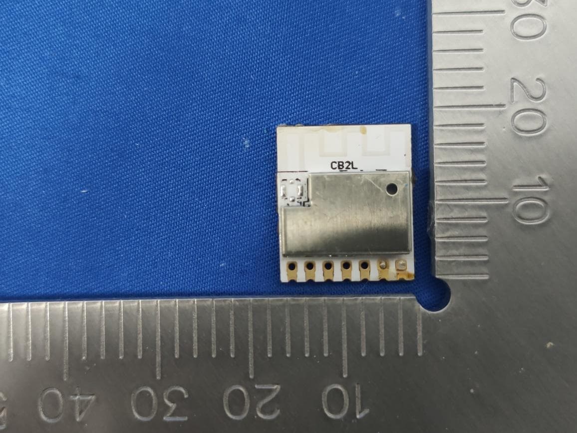
2AG94C-CB2L
Feb 23, 20222.4G Wifi & Bluetooth Module
Equipment Class
DTS - Digital Transmission System