2AHJ5-X3SEDesktop Terminal
EC Electronics, Limited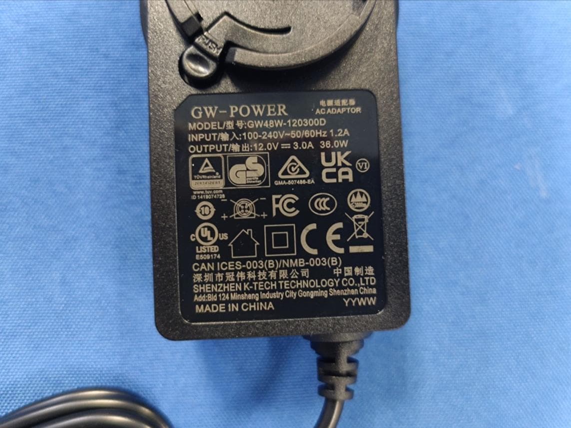
Click to zoom
Application Details
- Equipment Class
- DTS - Digital Transmission System
- Date of Grant
- Mar 09, 2026
- Application Purpose
- Original Equipment
- Equipment Note
- Desktop Terminal
- Frequency Range
- 2402.00000000 - 2480.00000000
- Company
- EC Electronics, Limited
- Country
- China
Documents & Files
Document Text
Text extracted from the exhibit documents filed with the FCC. Open a document above to read the original.
Users Manual
Safety and Usage Precautions Terms of Warranty Your hardware is covered for up to one year from the date of purchase. This limited warranty applies solely to you, the original purchaser, and is non-transferable to any subsequent owner, lessee, or recipient of the product. This warranty does not cover and we are not responsible for: Damages resulting from misuse, abuse, accidents, fire, theft, loss, or misplacement. Damage caused by power fluctuations, surges, or connections to improper voltage sources. Damage caused by viruses, malware, or malicious software. Damage resulting from reckless, willful, or intentional conduct. Damage due to servicing performed by unauthorized personnel. Damage caused by improper use inconsistent with product instructions or user manuals, including failure to perform necessary cleaning or preventive maintenance. Damage resulting from modifications to the product or its components without prior written approval. Normal wear and tear, including gradual image degradation, uneven screen aging, burn-in, or pixel failure within the product’s specified tolerances that do not significantly impair functionality. Software issues, including the operating system, pre-installed software, third-party applications, or reloaded software. Components or equipment not originally supplied with the product. Minor imperfections that meet design specifications. External appearance damage such as scratches, cracks, or other cosmetic issues that do not affect functionality. Missing, altered, or defaced serial numbers. Wireless data services provided by third-party providers. Damage caused during transportation or improper packaging when returning the product. Warranty Statement Do not use the device in environments containing combustible gases, vapors, or dusts. Non-professional users must not disassemble or repair the power adapter, as there is a risk of high-voltage electric shock. Avoid installation or operation during thunderstorms to prevent damage caused by lightning strikes. If overheating, smoke, or abnormal odors are detected, disconnect the power immediately. Do not operate the device in extreme environmental conditions such as very cold, hot, or humid environments. For cleaning, use a dry, soft cloth. If necessary, a surface cleaner spray can be applied after the device is powered off, ensuring no liquid enters the device. Avoid dropping or throwing the device. Handle with care and do not forcibly adjust the screen angle. Use the device in a clean, dust-free environment. Prevent the intrusion of small metal objects and insects into the device. Technical Data Android POS Terminal The pictures are for reference only; please prioritize practicality. User Manual Package Content Device Interfaces Introduction Please check the following parts before use: Host Computer Power Adapter 美团X3SE英文说明书(A4尺寸) 材质:A4纸,正反两面单黑打印 34 56 78 12 Startup Procedure Power Button Main Screen Designed for operator use. 1 2 2 3 3 Cable Management Bin All types of cables can be connected and routed through this bin. 1.Press the Power Button to power on the device. The display will activate. Upon initial boot, the startup interface will appear. Follow the on-screen prompts to proceed with operation. 2.The device supports two methods of internet connectivity: Wireless Connection: Select the desired wireless network from the available options on the welcome screen. Enter the network password when prompted to establish a connection. Wired Connection: Connect an Ethernet cable from the network source to the device’s network port to establish a wired connection. When the device is off, short press the button to turn it on. When the device is on: Long press for 4 seconds to initiate a soft power-off. Long press for 11 seconds to perform a hard power-off. Main Screen: 15.6’’,1366*768 G + G, 10 Point Touch Custom AOSP OS OS Storage Wi-Fi Bluetooth Display Parameter Touch Screen Speaker Overall Size Power Adapter Working Temperature Working Humidity Storage Temperature Storage Humidity 4GB RAM + 32GB ROM 2.4GHzIEEE 802.11 b/g/n Bluetooth 4.2 2W 380*340*180mm INPUT: 100-240V~ 50/60Hz OUTPUT: 12V 3A 10~90RH -20 C~60C -10 C~55C 20~80RH 1 Power Port Cashbox Port Electronic Scale Network Micro USB Debug Earphone TF Card Slot USB*2 USB*2 Power Button Main Screen Cable Management Bin Speaker SAA PLUGUL PLUGEU PLUGUK PLUG 90101-46900 FCC warning statements: This equipment has been tested and found to comply with the limits for a Class B digital device, pursuant to part 15 of the FCC Rules. These limits are designed to provide reasonable protection against harmful interference in a residential installation. This equipment generates, uses and can radiate radio frequency energy and, if not installed and used in accordance with the instructions, may cause harmful interference to radio communications. However, there is no guarantee that interference will not occur in a particular installation. If this equipment does cause harmful interference to radio or television reception, which can be determined by turning the equipment off and on, the user is encouraged to try to correct the interference by one or more of the following measures: • Reorient or relocate the receiving antenna. • Increase the separation between the equipment and receiver. • Connect the equipment into an outlet on a circuit different from that to which the receiver is connected. • Consult the dealer or an experienced radio/TV technician for help. Caution: Any changes or modifications to this device not explicitly approved by manufacturer could void your authority to operate this equipment. This device complies with part 15 of the FCC Rules. Operation is subject to the following two conditions: (1) This device may not cause harmful interference, and (2) this device must accept any interference received, including interference that may cause undesired operation. The device has been evaluated to meet general RF exposure requirement This equipment complies with FC…
Text truncated - open the document above for the full version.
Attestation Statements
EC Electronics, Limited Room 2A, 2/F., Mai Tak Industrial Building, 221 Wai Yip Street, Kwun Tong, Kowloon Hong Kong China Date: March 2, 2026 Federal Communications Commission Authorization and Evaluation Division 7435 Oakland Mills Road Columbia, MD 21046 FCC ID: 2AHJ5-X3SE FRN: 0025215401 US Agent – Attestation Statement / Part 2.911(d)(7) EC Electronics, Limited certifies, that as of March 2, 2026, we have designated FCC US Agent, LLC to accept service of process on our behalf for FCC ID: 2AHJ5-X3SE EC Electronics, Limited, accepts to maintain an agent of service of process in the United States for no less than one year after either the grantee has permanently terminated all marketing and importation of the applicable equipment within the U.S., or the conclusion of any Commission- related administrative or judicial proceeding involving the equipment, whichever is later. FCC US Agent, LLC, accepts as of the date of the filing of this application, the obligation of being the designated agent for the purpose of accepting service of process on behalf of EC Electronics, Limited for FCC ID: 2AHJ5-X3SE Designated Agent Information: Company Name: FCC US Agent, LLC FRN: 0033402884 Address: 3722 Illinois Avenue, Saint Charles, IL, 60174, USA Contact Person: Tim Payne Phone: 708-571-3148 Email: [email protected] Sincerely, Company: EC Electronics, Limited Designated Agent: FCC US Agent, LLC Company Representative: Eric Shiu Designated Agent Representative: Tim Payne Signature: Email: [email protected] Tel: (852) 3590 6397 Signature:
Attestation Statements
EC Electronics, Limited Covered Equipment Certification Attestation Letter 3/2/2026 Nemko North America, Inc. 303 River Road Ottawa K1V 1H2 Canada ATTN.: Reviewing Engineer FCC ID: 2AHJ5-X3SE EC Electronics, Limited (“ the applicant”) certifies that the equipment for which authorization is sought is not “covered” equipment prohibited from receiving an equipment authorization pursuant to section 2.903 of the FCC rules. Note: If the equipment for which the applicant seeks authorization is produced by any of the entities identified on the current Covered List, the applicant should include an explanation on why the equipment is not “covered” equipment. EC Electronics, Limited (“ the applicant”) certifies that, as of the date of the filing of the application, the applicant is not identified on the Covered List as an entity producing “covered” equipment. EC Electronics, Limited (“the applicant”) certifies that the equipment for which authorization is sought does not include cybersecurity or anti-virus software produced or provided by Kaspersky Lab, Inc. or any of its successors and assignees, including equipment with integrated Kaspersky Lab, Inc. (or any of its successors and assignees) cybersecurity or anti-virus software pursuant to DA-24-886 and KDB 986446 D01 Covered Equipment Guidance section B(2a). Signed: Printed name: Eric Shiu Title: Manager Company Name: EC Electronics, Limited Date: 3/2/2026
Cover Letter(s)
EC Electronics, Limited March 2, 2026 Equipment Autorisation Division Federal Communications Commission 7435 Oakland Mills Road Columbia, MD 21046 FCC ID: 2AHJ5-X3SE Product Name: Desktop Terminal Request for Confidentiality Pursuant to Sections 0.457 and 0.459 of the commissions rules, we hereby request that the following documents be held confidential: Schematics Long-term confidential Block diagram Long-term confidential Operation description Long-term confidential These materials contain trade secrets and proprietary information and are not customarily released to the public. The public disclosure of this information might be harmful to the company and provide unjustified benefits to our competitors. Signature: Name Eric Shiu Company Name EC Electronics, Limited Address Room 2A, 2/F., Mai Tak Industrial Building, 221 Wai Yip Street, Kwun Tong, Kowloon, Hong Kong, China Tel (852) 3590 6397 Fax (852) 3590 6397 Email [email protected]
Cover Letter(s)
EC Electronics, Limited Differences Description We EC Electronics, Limited state: Product name: Desktop Terminal Model: :X3SE, EC-MT-X3, MT-X3, X3 After verification there is no difference except for the name of the model. All models of PCB design, software, electric circuit, radio frequency characteristics, appearance are consistent. 2026-3-2 Name Eric Shiu Position Manager Company Name EC Electronics, Limited Address Room 2A, 2/F., Mai Tak Industrial Building, 221 Wai Yip Street, Kwun Tong, Kowloon, Hong Kong, China Tel (852) 3590 6397 Fax (852) 3590 6397 Email [email protected] (Signature)
External Photos
FCCID: 2AHJ5-X3SE FCCID: 2AHJ5-X3SE FCCID: 2AHJ5-X3SE FCCID: 2AHJ5-X3SE FCCID: 2AHJ5-X3SE
ID Label/Location Info
4.5cm 2.5cm Label Location FCC ID: 2AHJ5-X3SE EC Electronics, Limited Product name: Desktop Terminal Model No.: X3SE This device complies with Part 15 of the FCC Rules. Operation is subject to the following two conditions: (1) this device may not cause harmful interference, and (2) this device must accept any interference received, including interference that may cause undesired operation.
Internal Photos
FCCID: 2AHJ5-X3SE FCCID: 2AHJ5-X3SE FCCID: 2AHJ5-X3SE FCCID: 2AHJ5-X3SE FCCID: 2AHJ5-X3SE FCCID: 2AHJ5-X3SE FCCID: 2AHJ5-X3SE FCCID: 2AHJ5-X3SE FCCID: 2AHJ5-X3SE FCCID: 2AHJ5-X3SE FCCID: 2AHJ5-X3SE FCCID: 2AHJ5-X3SE ANT
RF Exposure Info
FCC ID: 2AHJ5-X3SE Prediction of MPE at a given distance 1. Limits The criteria listed in the following table shall be used to evaluate the environment impact of human exposure to radio frequency (RF) radiation as specified in 1.1307(b) 2. Test Procedure Equation from page 18 of OET Bulletin 65, Edition 97-01 Where: S = power density P = power input to the antenna G = numeric gain of the antenna in the direction of interest relative to an isotropic radiator R = distance to the centre of radiation of the antenna FCC ID: 2AHJ5-X3SE 3. Result Worse case is as below: Mode Frequency (MHz) Prediction distance (cm) RF output power MPE (mW/cm 2 ) Limit (mW/cm 2 ) MPE Test Exclusion dBm mW EDR 2402-2480 20 7.182 5.2264 0.00151 1 Yes BLE 2402-2480 20 4.965 3.1369 0.00090 1 Yes 2.4GWIFI 2412-2462 20 14.566 28.6154 0.00825 1 Yes Maximum Simultaneous transmission MPE Ratios for EDR+2.4GWIFI: Max MPE ratio EDR /Limit Max MPE ratio WIFI /Limit ∑MPE ratios Limit Result 0.00151 0.00825 0.00976 1 PASS EDR&BLE&2.4GWIFI Antenna Gain: 1.61dBi, 1.45(numeric) Meet MPE requirements, RF Exposure evaluation is not required.
Test Report
ALPHA's reports is using a digital certificate that is trusted on Adobe's official server. If there is no digital certificate or the digital certificate shows damaged in your report. Please do not accept the report. E-mail: [email protected] Tel: 400-8300-895 Website: http://www.a-lab.cn FCC TEST REPORT FCC ID: 2AHJ5-X3SE On Behalf of EC Electronics, Limited Desktop Terminal Model No.: X3SE, EC-MT-X3, MT-X3, X3 Prepared for : EC Electronics, Limited Address : Room 2A, 2/F., Mai Tak Industrial Building, 221 Wai Yip Street, Kwun Tong, Kowloon, Hong Kong, China Prepared By : Shenzhen Alpha Product Testing Co., Ltd. Address : Building i, No.2, Lixin Road, Fuyong Street, Bao'an District, 518103, Shenzhen, Guangdong, China Report Number : A2512080-C04-R02 Date of Receipt : December 10, 2025 Date of Test : December 10, 2025 – January 26, 2026 Date of Report : January 28, 2026 Version Number : V0 Result Pass Page 2 of 51 Report No.: A2512080-C04-R02 TABLE OF CONTENTS Description Page 1. Summary of Standards And Results ------------------------------------------------------------ 6 1.1. Description of Standards and Results ----------------------------------------------------- 6 2. General Information ---------------------------------------------------------------------------------- 7 2.1. Description of Device (EUT) ----------------------------------------------------------------- 7 2.2. Accessories of Device (EUT) ---------------------------------------------------------------- 8 2.3. Tested Supporting System Details---------------------------------------------------------- 8 2.4. Block Diagram of Test -------------------------------------------------------------------------- 8 2.5. Test Mode Description ------------------------------------------------------------------------- 9 2.6. Test Conditions ---------------------------------------------------------------------------------- 9 2.7. Test Facility --------------------------------------------------------------------------------------- 9 2.8. Measurement Uncertainty ------------------------------------------------------------------ 10 2.9. Test Equipment List--------------------------------------------------------------------------- 11 3. Spurious Emission ---------------------------------------------------------------------------------- 14 3.1. Test Limits --------------------------------------------------------------------------------------- 14 3.2. Test Procedure --------------------------------------------------------------------------------- 16 3.3. Test Setup --------------------------------------------------------------------------------------- 17 3.4. Test Results------------------------------------------------------------------------------------- 19 4. RF CONDUCTED SPURIOUS EMISSIONS -------------------------------------------------- 23 4.1. Block diagram of test setup ---------------------------------------------------------------- 23 4.2. Limits --------------------------------------------------------------------------------------------- 23 4.3. Test procedure --------------------------------------------------------------------------------- 23 4.4. Test result --------------------------------------------------------------------------------------- 23 5. Power line Conducted Emission --------------------------------------------------------------- 27 5.1. Test Limits --------------------------------------------------------------------------------------- 27 5.2. Test Procedure --------------------------------------------------------------------------------- 27 5.3. Test Setup --------------------------------------------------------------------------------------- 27 5.4. Test Results------------------------------------------------------------------------------------- 27 6. Duty Cycle --------------------------------------------------------------------------------------------- 30 6.1. Block diagram of test setup ---------------------------------------------------------------- 30 6.2. Test Procedure --------------------------------------------------------------------------------- 30 6.3. Test Results------------------------------------------------------------------------------------- 30 7. Conducted Maximum Output Power ---------------------------------------------------------- 33 7.1. Test limits ---------------------------------------------------------------------------------------- 33 7.2. Test Procedure --------------------------------------------------------------------------------- 33 7.3. Test Setup --------------------------------------------------------------------------------------- 33 7.4. Test Results------------------------------------------------------------------------------------- 33 8. Peak Power Spectral Density ------------------------------------------------------------------- 36 8.1. Test limits ---------------------------------------------------------------------------------------- 36 8.2. Test Procedure --------------------------------------------------------------------------------- 36 8.3. Test Setup --------------------------------------------------------------------------------------- 36 8.4. Test Results------------------------------------------------------------------------------------- 36 9. Bandwidth ---------------------------------------------------------------------------------------------- 39 9.1. Test limits ---------------------------------------------------------------------------------------- 39 9.2. Test Procedure --------------------------------------------------------------------------------- 39 9.3. Test Setup --------------------------------------------------------------------------------------- 39 9.4. Test Results------------------------------------------------------------------------------------- 39 Page 3 of 51 Report No.: A2512080-C04-R02 10. Band Edge (Conducted) -------------------------------------------------------------------------- 43 10.1. Test limits ----------------------------------…
Text truncated - open the document above for the full version.
Test Report
ALPHA's reports is using a digital certificate that is trusted on Adobe's official server. If there is no digital certificate or the digital certificate shows damaged in your report. Please do not accept the report. E-mail: [email protected] Tel: 400-8300-895 Website: http://www.a-lab.cn FCC TEST REPORT FCC ID: 2AHJ5-X3SE On Behalf of EC Electronics, Limited Desktop Terminal Model No.: X3SE, EC-MT-X3, MT-X3, X3 Prepared for : EC Electronics, Limited Address : Room 2A, 2/F., Mai Tak Industrial Building, 221 Wai Yip Street, Kwun Tong, Kowloon, Hong Kong, China Prepared By : Shenzhen Alpha Product Testing Co., Ltd. Address : Building i, No.2, Lixin Road, Fuyong Street, Bao'an District, 518103, Shenzhen, Guangdong, China Report Number : A2512080-C04-R03 Date of Receipt : December 10, 2025 Date of Test : December 10, 2025 – January 26, 2026 Date of Report : January 28, 2026 Version Number : V0 Result Pass Page 2 of 94 Report No.: A2512080-C04-R03 TABLE OF CONTENTS Description Page 1. Summary of Standards And Results -------------------------------------------------------------- 6 1.1. Description of Standards and Results ------------------------------------------------------- 6 2. General Information ------------------------------------------------------------------------------------ 7 2.1. Description of Device (EUT) ------------------------------------------------------------------- 7 2.2. Accessories of Device (EUT) ------------------------------------------------------------------ 8 2.3. Tested Supporting System Details------------------------------------------------------------ 8 2.4. Block Diagram of Test ---------------------------------------------------------------------------- 8 2.5. Test Mode Description --------------------------------------------------------------------------- 9 2.6. Test Conditions ---------------------------------------------------------------------------------- 10 2.7. Test Facility --------------------------------------------------------------------------------------- 10 2.8. Measurement Uncertainty -------------------------------------------------------------------- 11 2.9. Test Equipment List----------------------------------------------------------------------------- 12 3. Spurious Emission ------------------------------------------------------------------------------------ 15 3.1. Test Limits ----------------------------------------------------------------------------------------- 15 3.2. Test Procedure ----------------------------------------------------------------------------------- 18 3.3. Test Setup ----------------------------------------------------------------------------------------- 18 3.4. Test Results--------------------------------------------------------------------------------------- 19 4. RF CONDUCTED SPURIOUS EMISSIONS ---------------------------------------------------- 26 4.1. Block diagram of test setup ------------------------------------------------------------------ 26 4.2. Limits ----------------------------------------------------------------------------------------------- 26 4.3. Test procedure ----------------------------------------------------------------------------------- 26 4.4. Test result ----------------------------------------------------------------------------------------- 26 5. Power line Conducted Emission ----------------------------------------------------------------- 39 5.1. Test Limits ----------------------------------------------------------------------------------------- 39 5.2. Test Procedure ----------------------------------------------------------------------------------- 39 5.3. Test Setup ----------------------------------------------------------------------------------------- 39 5.4. Test Results--------------------------------------------------------------------------------------- 39 6. Duty Cycle ----------------------------------------------------------------------------------------------- 42 6.1. Block diagram of test setup ------------------------------------------------------------------ 42 6.2. Test Procedure ----------------------------------------------------------------------------------- 42 6.3. Test Results--------------------------------------------------------------------------------------- 42 7. Conducted Maximum Output Power ------------------------------------------------------------ 49 7.1. Test limits ------------------------------------------------------------------------------------------ 49 7.2. Test Procedure ----------------------------------------------------------------------------------- 49 7.3. Test Setup ----------------------------------------------------------------------------------------- 49 7.4. Test Results--------------------------------------------------------------------------------------- 50 8. Peak Power Spectral Density --------------------------------------------------------------------- 57 8.1. Test limits ------------------------------------------------------------------------------------------ 57 8.2. Test Procedure ----------------------------------------------------------------------------------- 57 8.3. Test Setup ----------------------------------------------------------------------------------------- 57 8.4. Test Results--------------------------------------------------------------------------------------- 58 9. Bandwidth ------------------------------------------------------------------------------------------------ 65 9.1. Test limits ------------------------------------------------------------------------------------------ 65 Page 3 of 94 Report No.: A2512080-C04-R03 9.2. Test Procedure ----------------------------------------------------------------------------------- 65 9.3. Test Setup ----------------------------------------------------------------------------------------- 65 9.4. Test Results--------------------------------------------------------------------------------------- 65 10. Band Edge (Conducted) ----------------------------------------…
Text truncated - open the document above for the full version.
Test Report
Page 71 of 94 Report No.: A2512080-C04-R03 -6dB Bandwidth NVNT n40 2452MHz Ant1 Page 72 of 94 Report No.: A2512080-C04-R03 Occupied Channel Bandwidth Condition Mode Frequency (MHz) Antenna 99% OBW (MHz) NVNT b 2412 Ant1 14.775 NVNT b 2437 Ant1 14.805 NVNT b 2462 Ant1 14.805 NVNT g 2412 Ant1 16.573 NVNT g 2437 Ant1 16.663 NVNT g 2462 Ant1 16.603 NVNT n20 2412 Ant1 17.742 NVNT n20 2437 Ant1 17.712 NVNT n20 2462 Ant1 17.712 NVNT n40 2422 Ant1 35.904 NVNT n40 2437 Ant1 35.964 NVNT n40 2452 Ant1 35.904 OBW NVNT b 2412MHz Ant1 OBW NVNT b 2437MHz Ant1 Page 73 of 94 Report No.: A2512080-C04-R03 OBW NVNT b 2462MHz Ant1 OBW NVNT g 2412MHz Ant1 Page 74 of 94 Report No.: A2512080-C04-R03 OBW NVNT g 2437MHz Ant1 OBW NVNT g 2462MHz Ant1 Page 75 of 94 Report No.: A2512080-C04-R03 OBW NVNT n20 2412MHz Ant1 OBW NVNT n20 2437MHz Ant1 Page 76 of 94 Report No.: A2512080-C04-R03 OBW NVNT n20 2462MHz Ant1 OBW NVNT n40 2422MHz Ant1 Page 77 of 94 Report No.: A2512080-C04-R03 OBW NVNT n40 2437MHz Ant1 OBW NVNT n40 2452MHz Ant1 Page 78 of 94 Report No.: A2512080-C04-R03 Page 79 of 94 Report No.: A2512080-C04-R03 10. BAND EDGE (CONDUCTED) 10.1.Test limits In any 100 kHz bandwidth outside the frequency band in which the spread spectrum or digitally modulated intentional radiator is operating, the radio frequency power that is produced by the intentional radiator shall be at least 20 dB below that in the 100 kHz bandwidth within the band that contains the highest level of the desired power, based on either an RF conducted or a radiated measurement, provided the transmitter demonstrates compliance with the peak conducted power limits. If the transmitter complies with the conducted power limits based on the use of RMS averaging over a time interval, as permitted under paragraph (b)(3) of this section, the attenuation required under this paragraph shall be 30 dB instead of 20 dB. Attenuation below the general limits specified in § 15.209(a) is not required. In addition, radiated emissions which fall in the restricted bands, as defined in § 15.205(a), must also comply with the radiated emission limits specified in § 15.209(a) (see § 15.205(c)). 10.2.Block diagram of test setup 10.3.Test Procedure Details see the ANSI C63.10-2020 + Cor. 1-2023 + C63.10a-2024 + Errata to C63.10a-2024 10.3.1. Place the EUT on the table and set it in transmitting mode. 10.3.2. Remove the antenna from the EUT and then connect a low loss RF cable from the antenna port to the spectrum analyzer. 10.3.3. Set center frequency of spectrum analyzer = operating frequency. 10.3.4. The resolution bandwidth is set to 100 kHz. The video bandwidth is set to 300 kHz. The detector is set to Peak. The trace mode is max hold. 10.3.5. Repeat above procedures until all frequency measured were complete. 10.4.Test Results PASS. Detailed information please see the following page. Page 80 of 94 Report No.: A2512080-C04-R03 Band Edge NVNT b 2412MHz Ant1 Ref Band Edge NVNT b 2412MHz Ant1 Emission Band Edge NVNT b 2462MHz Ant1 Ref Page 81 of 94 Report No.: A2512080-C04-R03 Band Edge NVNT b 2462MHz Ant1 Emission Band Edge NVNT g 2412MHz Ant1 Ref Page 82 of 94 Report No.: A2512080-C04-R03 Band Edge NVNT g 2412MHz Ant1 Emission Band Edge NVNT g 2462MHz Ant1 Ref Page 83 of 94 Report No.: A2512080-C04-R03 Band Edge NVNT g 2462MHz Ant1 Emission Band Edge NVNT n20 2412MHz Ant1 Ref Page 84 of 94 Report No.: A2512080-C04-R03 Band Edge NVNT n20 2412MHz Ant1 Emission Band Edge NVNT n20 2462MHz Ant1 Ref Page 85 of 94 Report No.: A2512080-C04-R03 Band Edge NVNT n20 2462MHz Ant1 Emission Band Edge NVNT n40 2422MHz Ant1 Ref Page 86 of 94 Report No.: A2512080-C04-R03 Band Edge NVNT n40 2422MHz Ant1 Emission Band Edge NVNT n40 2452MHz Ant1 Ref Page 87 of 94 Report No.: A2512080-C04-R03 Band Edge NVNT n40 2452MHz Ant1 Emission Page 88 of 94 Report No.: A2512080-C04-R03 11. BAND EDGE(RADIATED) 11.1.Test limits Please refer RSS-GEN & FCC PART 15: 15.247 In any 100 kHz bandwidth outside the frequency band in which the spread spectrum or digitally modulated device is operating, the RF power that is produced shall be at least 20 dB below that in the 100 kHz bandwidth within the band that contains the highest level of the desired power, based on either an RF conducted or a radiated measurement, provided that the transmitter demonstrates compliance with the peak conducted power limits. If the transmitter complies with the conducted power limits based on the use of root-mean-square averaging over a time interval, as permitted under section 5.4(d), the attenuation required shall be30 dB instead of 20 dB. Attenuation below the general field strength limits specified in RSS-Gen is not required. In addition, radiated emissions which fall in the restricted bands, as defined in Section 15.205(a), must also comply with the radiated emission limits specified in Section 15.209(a) (see Section 15.205(c)). 11.2.Block diagram of test setup Page 89 of 94 Report No.: A2512080-C04-R03 11.3.Test Procedure Details see the ANSI C63.10-2020 + Cor. 1-2023 + C63.10a-2024 + Errata to C63.10a-2024 11.3.1 Put the EUT on a 1.5m high table, power on the EUT. Emissions were scanned and measured rotating the EUT to 360 degrees, Find the maximum Emission 11.3.2 Check the spurious emissions out of band. 11.3.3 RBW 1MHz , VBW 3MHz , peak detector for peak value , RBW 1MHz , VBW 3MHz , RMS detector for AV value. All restriction band and non- restriction band have been tested, only worse case is reported. 11.4.Test Results PASS. Detailed information please see the following page. Page 90 of 94 Report No.: A2512080-C04-R03 Test Mode: IEEE 802.11b-Low Test Mode: IEEE 802.11…
Text truncated - open the document above for the full version.
Contact Information
Applicant
Eric Shiu
[email protected]Fax: (852) 3590 6497
Technical Contact
FCC US Agent, LLCTim Payne
3722 Illinois Avenue, Saint Charles, IL · Saint charles, Illinois, 60174 · United States
Test Firm
Shenzhen Alpha Product Testing Co., LTD.Real Yak
Technical Specifications
| # | Rule Parts | Frequency Range | Power Output |
|---|---|---|---|
| 1 | 15C | 2.40 GHz - 2.48 GHz | 3.14 mW |
| 2 | 15C | 2.41 GHz - 2.46 GHz | 28.62 mW |
Other Applications from EC Electronics, Limited
2AHJ5-S5SPRO
Mar 18, 20262AHJ5-S5SPRO
Equipment Class
NII - Unlicensed National Information Infrastructure TX