2AMPF-MX2311NEO
MatchX GmbH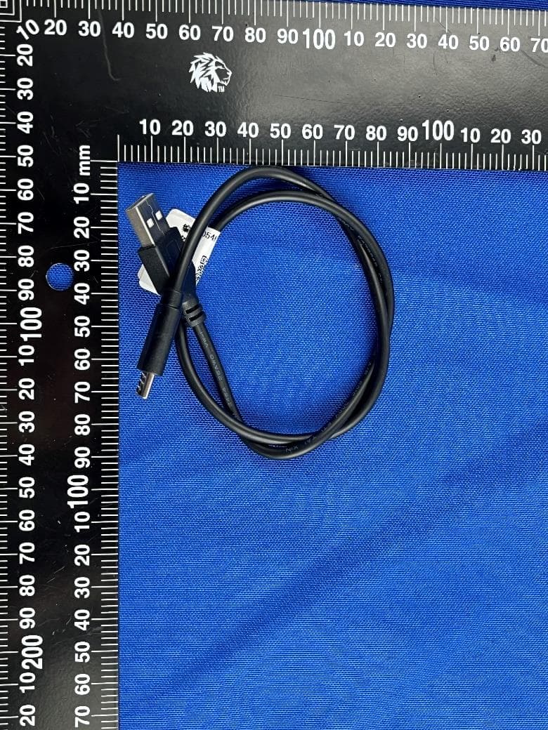
Click to zoom
Application Details
- Equipment Class
- DTS - Digital Transmission System
- Date of Grant
- Apr 04, 2023
- Application Purpose
- Original Equipment
- Date of Application
- Apr 04, 2023
- Equipment Note
- NEO
- Frequency Range
- 2412.00000000 - 2462.00000000
- Company
- MatchX GmbH
- Country
- Germany
Documents & Files
Document Text
Text extracted from the exhibit documents filed with the FCC. Open a document above to read the original.
Users Manual
2.4GHz LoRa Gateway NEO User Guide Copyright © 2023 MatchX Inc./MatchX GmbH WWW.MATCHX.IO No part of the specifications may be reproduced in any form or by any means or used to make any derivative such as translation, transformation, or adaptation without permission from MatchX Inc./MatchX GmbH All rights reserved. Release 1.0, February 2023 Contents 1Introduction. . . . . . . . . . . . . . . . . . . . . . . . . . . . . . . . . . . . . . . . . . . . . . . . . . . . 5 1.1Product overview5 1.2Features List5 1.2.1 WiFi . . . . . . . . . . . . . . . . . . . . . . . . . . . . . . . . . . . . . . . . . . . . . . . . . . . . . . . . . . . . . 5 1.2.2 LoRa . . . . . . . . . . . . . . . . . . . . . . . . . . . . . . . . . . . . . . . . . . . . . . . . . . . . . . . . . . . . 6 1.2.3 Processor subsystem . . . . . . . . . . . . . . . . . . . . . . . . . . . . . . . . . . . . . . . . . . . . . . . 6 1.3Connectors and Interfaces7 1.3.1 Led status . . . . . . . . . . . . . . . . . . . . . . . . . . . . . . . . . . . . . . . . . . . . . . . . . . . . . . . . 7 1.3.2 Console access . . . . . . . . . . . . . . . . . . . . . . . . . . . . . . . . . . . . . . . . . . . . . . . . . . . 7 2Quick Installation Guide. . . . . . . . . . . . . . . . . . . . . . . . . . . . . . . . . . . . . . . . 8 2.1Software requirements8 2.2Hardware requirements8 2.3Power connection9 2.4Accessing the Gateway and Internet connection9 2.4.1 Ethernet connection . . . . . . . . . . . . . . . . . . . . . . . . . . . . . . . . . . . . . . . . . . . . . . . 9 2.4.2 WiFi connection . . . . . . . . . . . . . . . . . . . . . . . . . . . . . . . . . . . . . . . . . . . . . . . . . . 10 3Product specification. . . . . . . . . . . . . . . . . . . . . . . . . . . . . . . . . . . . . . . . . . 11 3.1Hardware Specification11 3.2WiFi specification12 3.3LoRa Radio specification12 4Package content. . . . . . . . . . . . . . . . . . . . . . . . . . . . . . . . . . . . . . . . . . . . . . 13 5Revision History. . . . . . . . . . . . . . . . . . . . . . . . . . . . . . . . . . . . . . . . . . . . . . . . 14 6Important Notice. . . . . . . . . . . . . . . . . . . . . . . . . . . . . . . . . . . . . . . . . . . . . . 15 6.1Legal notice15 6.2CE regulatory conformance - applies to MX231115 6.3FCC regulatory conformance - applies to MX231116 6.4IC regulatory conformance - applies to MX231116 1. Introduction 1.1 Product overview The MX2311 is an indoor ultra-low power gateway, equipped with the SX1280 chip to provide connectivity between low-power devices and the Supernode. It operates on the 2.4GHz frequency band and utilizes LoRa modulation for long-range, low-power wireless communication, making it well-suited for indoor use. With multiple physical layers and modulations, the MX2311 is optimized for long-range communication at high data rates and has a coverage of up to 4 km. As a gateway, it is capable of data transfer, processing, and authentication, making it a versatile solution for indoor IoT networks. 1.2 Features List • LoRa 2.4GHz. • WiFi with full function of 802.11b/g/n over 2.4GHz. • Two Built-in PCB Antennas for LoRa and WiFi communication. • 10/100 Mbps Ethernet connection. • Internal Flash memory. • USB-C interface for power and debug. • Internal storage 4GB eMMC Flash • Secure element for authentication. • Auto diagnostic functions. • Average Low power consumption less than 1W. • IP52 indoor enclosure. • Temperature ranges from -10 ◦ C to 60 ◦ C. 1.2.1 WiFi The MX2311 Gateway is equipped with built-in WiFi connectivity according to the 2.4GHz 802.11b/g/n specification. It has a built-in antenna, so no additional installation is required. The 6Chapter 1. Introduction WiFi connection can be used to provide internet access to the Gateway or to access the Web UI configuration page to manage the Gateway. If WiFi is not needed, it can be disabled to save power. 1.2.2 LoRa It provides long range communication in the 2.4GHz band with the linearity to withstand heavy interference. The transceiver’s high sensitivity and high efficiency power amplifier allows it to de- modulate more data packets, reducing data collisions and allowing for more dense sensor deployment in applications such as smart farming, home automation, and asset tracking. This enables a higher degree of connectivity and control, making it possible to monitor and manage a larger number of devices or assets in a given area. Additionally, the support for different modulation schemes and programmable bit rate allows for flexibility and adaptability in different use cases and environments. 1.2.3 Processor subsystem The MX2311 Gateway is based on the MT7688AN SoC, which is a system-on-chip developed by MediaTek. This SoC is designed for Internet of Things (IoT) applications and features a 580 MHz CPU equipped with 128MB of DDR2 and 32MB Internal flash. Figure 1.1: Connectors and Interfaces of the Gateway. 1.3 Connectors and Interfaces7 1.3 Connectors and Interfaces The following interfaces are available, (see Figure 1.1): 1. User button - Is used to reset the Gateway to the factory settings. 2. Ethernet Connector. 3.USB-C Connector - The main function is to power the Gateway and can be used for accessing the console terminal. 4. NEO LED - It is an indicator for the Gateway activity. 5.Indicator RGB LED - It is used as a description of the possible status that can be found in the Table 1.1. 1.3.1 Led status The Gateway uses an RGB LED to indicate a various status and its condition. Description of the LED status can be found in Table 1.1. 1.3.2 Console access By default the console terminal of the Gateway can be accessed through the USB-C connector. Internally CH340C UART-USB converter is used, if the drivers for this device are not automatically installed on the PC operating system they can be downloaded from WCH Website. The PC should detect the Gateway as a Virtual COM port. Any terminal software capable of communicating through COM ports can be used e.g. PuTTY or RealTerm. The default…
Text truncated - open the document above for the full version.
Attestation Statements
MatchX GmbH Federal Communications Commission Authorization and Evaluation Division 7435 Oakland Mills Road Columbia, MD 21046 USA Date: 3-21-2023 Ref: Attestation Statements Part 2.911(d)(5)(ii) Filing FCC ID: 2AMPF-MX2311 MatchX GmbH certifies that, as of the date of the filing of the application, the applicant is not identified on the Covered List as an entity producing “covered” equipment. Sincerely, Xin Hu Rev 1/26/2023
Attestation Statements
MatchX GmbH Federal Communications Commission Authorization and Evaluation Division 7435 Oakland Mills Road Columbia, MD 21046 USA Date: 3-21-2023 Ref: Attestation Statements Part 2.911(d)(5)(i) Filing FCC ID: 2AMPF-MX2311 MatchX GmbH certifies that the equipment for which authorization is sought is not “covered” equipment prohibited from receiving an equipment authorization pursuant to section 2.903 of the FCC rules. Sincerely, Xin Hu Rev 1/26/2023
Attestation Statements
MatchX GmbH Tempelhofer Ufer 17 Berlin, 10963 Germany Date: March 29, 2023 Federal Communications Commission Authorization and Evaluation Division 7435 Oakland Mills Road Columbia, MD 21046 FCC ID: 2AMPF-MX2311 US Agent – Attestation Statement / Part 2.911(d)(7) MatchX GmbH certifies, that as of March 29, 2023, we have designated FCC US Agent, LLC to accept service of process on our behalf for FCC ID: 2AMPF-MX2311. MatchX GmbH, accepts to maintain an agent of service of process in the United States for no less than one year after either the grantee has permanently terminated all marketing and importation of the applicable equipment within the U.S., or the conclusion of any Commission- related administrative or judicial proceeding involving the equipment, whichever is later. FCC US Agent, LLC, accepts as of the date of the filing of this application, the obligation of being the designated agent for the purpose of accepting service of process on behalf of MatchX GmbH for FCC ID: 2AMPF-MX2311. Designated Agent Information: Company Name: FCC US Agent, LLC Address: 3722 Illinois Avenue, Saint Charles, IL, 60174, USA FRN: 0033402884 Contact Person: Tim Payne Phone: 708-571-3148 Email: [email protected] Sincerely, Company: MatchX GmbHDesignated Agent: FCC US Agent, LLC Company Representative: Xin HuDesignated Agent Representative: Tim Payne Signature: Signature:
Cover Letter(s)
MatchX GmbH Agent Authorization Company: MatchX GmbH Address: Tempelhofer Ufer 17, 10963 Berlin, Germany Product Name: Neo Model Number(s): MX2311 Product Description: NEO We authorize MiCOM Labs Inc., 575 Boulder Court, Pleasanton, California 94566, USA, to act on our behalf on all matters concerning the certification of above named equipment. We declare that MiCOM Labs Inc. is allowed to forward all information related to the approval and certification of equipment to the regulatory agencies as required and to discuss any issues concerning the approval application. Any and all acts carried out by MiCOM Labs on our behalf shall have the same effect as acts of our own. Signature: Date: 2023-04-03 Name: Xin Hu Title: Manager Company: MatchX GmbH
Cover Letter(s)
Date: 21 March 2023 MatchX GmbH To:Federal Communications Commission, Authorization & Evaluation Division, 7435 Oakland Mills Road, Columbia, MD 21046 To Whom It May Concern: The MatchX GmbH, the undersigned, hereby authorizes Mr. Wu Xuewen from Shenzhen BALUN Technology Co., Ltd., to act on the behalf of the MatchX GmbH solely in matters relating to the application for an FCC equipment authorization for FCC ID:2AMPF-MX2311 including the signing of documents in connection with this Application. Necessary acts carried out by Shenzhen BALUN Technology Co., Ltd. in connection with the Application shall have the same effect as acts of the MatchX GmbH. The MatchX GmbH also hereby certify that no party to this application is subject to a denial of benefits, including FCC benefits, pursuant to Section 5301 of the Anti-Drug Abuse Act of 1988, 21 U.S.C. Section 862. Yours Sincerely, _______ Xin Hu
Cover Letter(s)
Date: 21 March 2023 MatchX GmbH To: Federal Communications Commission, Authorization & Evaluation Division, 7435 Oakland Mills Road, Columbia, MD 21046 Re: MatchX GmbH FCC ID: 2AMPF-MX2311 FCC Certification Confidentiality Request Gentlemen: This letter is to comply with 47 CFR 0.457 and 0.459 pertaining to confidentiality material. MatchX GmbH requests that the following documents regarding this submission for FCC ID: 2AMPF-MX2311 be kept confidential: Exhibit TypeFile Name Block DiagramBlock Diagram.pdf SchematicsSchematics.pdf Operational DescriptionOperational Description.pdf And below exhibit kept short-term confidential (180 days): External photosExternal photos.pdf Test setup photostest photo.pdf Internal photosInternal photos.pdf User manualUser manual.pdf Those documents contain detailed system and equipment description and related information about the product which MatchX GmbH considers to be confidential proprietary, a custom design and, otherwise, not releasable to the general public. Since this design is a basis form which future technological products will evolve, MatchX GmbH considers this information would be of benefit to its competitors, and that the disclosure of the information in these documents would give competitors an unfair advantage in the market. Yours Sincerely, Xin Hu
External Photos
Report No.: BL-SZ2320945-AW 1 / 4 EUT EXTERNAL PHOTOS FRONT VIEW OF EUT REAR VIEW OF EUT .3 Report No.: BL-SZ2320945-AW 2 / 4 LEFT VIEW OF EUT CLOSE-UP Report No.: BL-SZ2320945-AW 3 / 4 RIGHT VIEW OF EUT TOP VIEW OF EUT Report No.: BL-SZ2320945-AW 4 / 4 BOTTOM VIEW OF EUT Accessory-Type-C Cable --BLANK BELOW--
ID Label/Location Info
Label: Location:
Internal Photos
Report No.: BL-SZ2320945-AI 1 / 3 1 EUT INTERNAL PHOTOS EUT UNCOVER VIEW 1 EUT UNCOVER VIEW 2 Report No.: BL-SZ2320945-AI 2 / 3 MAIN BOARD TOP VIEW (WITH SHIELDING) MAIN BOARD TOP VIEW (WITHOUT SHIELDING) PCB Antenna RF Chip Report No.: BL-SZ2320945-AI 3 / 3 MAIN BOARD REAR VIEW --BLANK BELOW--
Test Report
Application Report 2.4-GHz Inverted F Antenna ABSTRACT This document describes a printed-circuit board (PCB) antenna design that can be used with all 2.4-GHz transceivers and transmitters from Texas Instruments ™ . The maximum gain when used on the reference board is measured to be +3.3 dBi, and the overall size requirements for this antenna are 25.7 × 7.5 mm (not including ground plane). Table of Contents 1 Description of the antenna Design........................................................................................................................................2 2 Measurement Results.............................................................................................................................................................3 2.1 Radiation Pattern...............................................................................................................................................................3 2.2 Reflection.........................................................................................................................................................................10 2.3 Bandwidth.........................................................................................................................................................................11 3 Summary................................................................................................................................................................................11 4 References.............................................................................................................................................................................11 5 Revision History...................................................................................................................................................................12 Trademarks Texas Instruments ™ is a trademark of Texas Instruments. All trademarks are the property of their respective owners. www.ti.comTable of Contents SWRU120D – APRIL 2007 – REVISED JANUARY 2019 Submit Document Feedback 2.4-GHz Inverted F Antenna1 Copyright © 2021 Texas Instruments Incorporated 1 Description of the antenna Design It is important to make an exact copy of the antenna dimensions to obtain optimum performance. The easiest approach to implement the antenna in a PCB CAD tool is to import the antenna layout from a gerber file or a DXF file. Such files are included in CC2430DB reference design [1]. The gerber file is called Inverted_F_Antenna.spl and the DXF file is called Inverted_F_Antenna.dxf. If the antenna is implemented on a PCB that is wider than the antenna, avoid placing components or having a ground plane close to the end points of the antenna. If the CAD tool being used does not support importing gerber or DXF files, see Figure 1-1 and Table 1-1. The antenna impedance is tuned to 50 ohm on the reference board. The impedance will however be affected by different size and shape of the ground plane, objects in the antenna nearfield such as mechanical assemblies (housing, batteries, etc.), PCB thickness, PCB material and so on. It is therefore recommended to add a pi-network close to the antenna feedpoint for impedance matching. The results presented in this document are based on an antenna implemented on a PCB with a 1-mm thickness using standard FR-4 material. Figure 1-1. IFA Dimensions Table 1-1. IFA Dimensions H15.70 mmW20.46 mm H20.74 mmL125.58 mm H31.29 mmL216.40 mm H42.21 mmL32.18 mm H50.66 mmL44.80 mm H61.21 mmL51.00 mm H70.80 mmL61.00 mm H81.80 mmL73.20 mm H90.61 mmL80.45 mm W11.21 mm Description of the antenna Designwww.ti.com 22.4-GHz Inverted F AntennaSWRU120D – APRIL 2007 – REVISED JANUARY 2019 Submit Document Feedback Copyright © 2021 Texas Instruments Incorporated 2 Measurement Results All of the results presented in this section are based on measurements performed with the CC2430DB [1] evaluation board. 2.1 Radiation Pattern Figure 2-1 shows how to relate all of the radiation patterns to the orientation of the antenna. The radiation patterns were measured with the CC2430 device programmed to 0-dBm output power. Figure 2-1. Relating Antenna to Radiation Patterns www.ti.comMeasurement Results SWRU120D – APRIL 2007 – REVISED JANUARY 2019 Submit Document Feedback 2.4-GHz Inverted F Antenna3 Copyright © 2021 Texas Instruments Incorporated Figure 2-2 shows the XY plane vertical polarization. Figure 2-2. XY Plane–Vertical Polarization Measurement Resultswww.ti.com 42.4-GHz Inverted F AntennaSWRU120D – APRIL 2007 – REVISED JANUARY 2019 Submit Document Feedback Copyright © 2021 Texas Instruments Incorporated Figure 2-3 shows the XY plane horizontal polarization. Figure 2-3. XY Plane–Horizontal Polarization www.ti.comMeasurement Results SWRU120D – APRIL 2007 – REVISED JANUARY 2019 Submit Document Feedback 2.4-GHz Inverted F Antenna5 Copyright © 2021 Texas Instruments Incorporated Figure 2-4 shows the XZ plane vertical polarization. Figure 2-4. XZ Plane–Vertical Polarization Measurement Resultswww.ti.com 62.4-GHz Inverted F AntennaSWRU120D – APRIL 2007 – REVISED JANUARY 2019 Submit Document Feedback Copyright © 2021 Texas Instruments Incorporated Figure 2-5 shows the XZ plane horizontal polarization. Figure 2-5. XZ Plane–Horizontal Polarization www.ti.comMeasurement Results SWRU120D – APRIL 2007 – REVISED JANUARY 2019 Submit Document Feedback 2.4-GHz Inverted F Antenna7 Copyright © 2021 Texas Instruments Incorporated Figure 2-6 shows the YZ plane vertical polarization. Figure 2-6. YZ Plane–Vertical Polarization Measurement Resultswww.ti.com 82.4-GHz Inverted F AntennaSWRU120D – APRIL 2007 – REVISED JANUARY 2019 Submit Document Feedback Copyright © 2021 Texas Instruments Incorporated Figure 2-7 shows the YZ plane horizontal polarization. Figure 2-7. YZ Plane–Horizontal Polarization www.ti.comMeasurement Results SWRU120D – APRIL 2007 – REVISED JANUARY 2019 Submit Document Feedback 2.4-GHz Inverted F Antenna9 Copyright © 202…
Text truncated - open the document above for the full version.
Test Report
Design Note DN024 SWRA227E Page 1 of 16 Monopole PCB Antenna with Single or Dual Band Option By Richard Wallace Keywords Single Band Mode (868 MHz, 915 MHz or 920 MHz) Dual Band Mode (868 MHz & 2440 MHz) PCB Antenna Monopole Antenna Excellent Efficiency Recommended Antenna Design for 868 MHz, 915 MHz & 920 MHz OTA Measurements 1 Introduction This document describes a PCB antenna that can be configured in two different modes of operation: the antenna can be tuned for a single frequency for operation in the 868 MHz (Europe), 915 MHz (USA) and 920 MHz (Japan) ISM bands; or the antenna can be configured as a dual band antenna which can operate at 868 MHz and 2440 MHz. This antenna can be used with all transceivers and transmitters from Texas Instruments which operates in these frequency bands. Overall size requirements for this antenna are 38 x 25 mm. Thus this is a medium size, low cost antenna solution. Figure 1 shows a picture the board being used to develop and characterize this antenna. This antenna design is one of the several antenna reference designs available on www.ti.com/lpw and is included in the Comprehensive Antenna Selection Guide [6] and the Antenna Selection Quick Guide [7]. Figure 1. CC-Antenna-DK, Board #6 PCB Monopole Antenna Design Note DN024 SWRA227E Page 2 of 16 Table of Contents KEYWORDS 1 1 INTRODUCTION 1 2 ABBREVIATIONS 2 3 DESCRIPTION OF THE PCB ANTENNA 3 3.1 IMPLEMENTATION OF THE MEANDERING MONOPOLE ANTENNA 3 4 RESULTS 5 4.1 RADIATION PATTERN 5 4.2 SINGLE BAND OPTION DESIGN FOR 868 / 915 / 920 MHZ 6 4.2.1 Antenna Match 6 4.2.1.1 Smith Chart – No Antenna Match Components 6 4.2.1.2 Theoretical Smith Chart Match 7 4.2.2 Bandwidth 8 4.3 DUAL BAND OPTION DESIGN FOR 868 & 2440 MHZ 9 4.3.1 Antenna Match 9 4.3.1.1 Smith Chart – No Antenna Match Components 9 4.3.2 Bandwidth 12 4.4 OTA MEASUREMENT SUMMARY 13 5 CONCLUSION 14 6 REFERENCES 15 7 DOCUMENT HISTORY 16 2 Abbreviations AUT Antenna Under Test BOM Bill Of Materials BW Bandwidth CF Correction Factor CITA Cellular Telecommunications Industry Association DK Development Kit EB Evaluation Board EIRP Effective Isotropic Radiated Power EM Evaluation Module ISM Industrial, Scientific, Medical NC Not Connected NHPRP Near Horizon Partial Radiated Power NHPRP45 Near Horizon Partial Radiated Power within 45 degrees angle OTA Over The Air PCB Printed Circuit Board RF Radio Frequency SWR Standing Wave Ratio TRP Total Radiated Power Design Note DN024 SWRA227E Page 3 of 16 3 Description of the PCB Antenna The antenna described in this document is a meandering monopole. The impedance of this antenna depends on the mode used. Referring to Figure 2, if the length of L4 is kept as shown then this is beneficial for the Dual Band Mode. If L4 is shortened to the silkscreen marking, then this is beneficial for the Single Band Mode. It is recommended to use a pi-matching network at the feed point of the antenna as shown in Figure 2 since the geometry of the ground plane affects the impedance of the antenna. The pi- network can be used to compensate for detuning caused by plastic encapsulation and other objects in close vicinity of the antenna. For further information on impedance matching and impedance measurements, see AN058 [6]. The antenna layout is positioned on the top and bottom layer of the board; this enables a lower resistive loss and gives a slightly wider bandwidth compared to a single sided layout solution. With a single sided layout; the area underneath the antenna can not be used for any other routing so it is more useful to utilize this area to optimize the antenna’s performance. 3.1 Implementation of the Meandering Monopole Antenna To obtain optimum performance it is important to make an exact copy of the antenna dimensions. The antenna was implemented on a 1.6 mm thick FR4 substrate. Since there is no ground plane beneath the antenna the PCB thickness is not critical, but if a different thickness is being used it will be necessary to change the matching network to obtain optimum performance. One approach to implement the antenna in a PCB CAD tool is to import the antenna layout from a Gerber file. Such a file is included in the CC-Antenna-DK Reference Design [8]. The CC-Antenna-DK contains 16 different board designs [1] and the gerbers from board 6 can be copied for this antenna design. If the antenna is implemented on a PCB that is wider than the antenna it is important to avoid placing components or having a ground plane close to each side of the antenna. If the CAD tool being used does not support import of Gerber files, Figure 2 and Table 1 can be used. Design Note DN024 SWRA227E Page 4 of 16 Figure 2. Antenna Dimensions L1 9.0 mm Y 43.0 mm L2 18.0 mm X1 63.0 mm L3 3.0 mm X2 25.0 mm L4 38.0 mm W 2.0 mm L5 1.0 mm Table 1. Antenna Dimensions Optimum length for the last antenna segment is dependent on the geometry of the ground plane. The antenna can also be used for 915 & 920 MHz. For larger ground planes L4 would have to be further reduced or the antenna match re-calculated. Design Note DN024 SWRA227E Page 5 of 16 4 Results The CTIA measurement summary results are presented in this section. Note that the performance will be affected by the size and shape of the ground plane. 4.1 Radiation Pattern Figure 3 and Figure 4 shows how to relate the radiation patterns in this section to the orientation of the antenna. A link to the full measurement report is included in the measurement summary. For reference purposes; measurements have also been performed on the standard whip SMA antennas that are supplied with the EM boards [3], [4]. Note that the size of the ground plane will affect the radiation pattern. Thus implementing this antenna on a board with a different size and shape of the ground plane will most likely affect the radiation pattern. Figure 3. Coordinates for the Radiation Patterns when used as a stand alone board Figure 4. Coordinates for the Radiation Patterns when used with the EM & EB Design Note DN02…
Text truncated - open the document above for the full version.
Test Report
Report No.: BL-SZ2320945-601 Tel: +86-755-66850100 E-mail: [email protected] Page No. 1 / 67 Web: www.titcgroup.com Template No.: TRP-FCC&ISED .247 (2022-01-12) Add: Block B, 1/F, Baisha Science and Technology Park, Shahe Xi Road, Nanshan District, Shenzhen, Guangdong Province, P. R. China TEST REPORT Applicant: MatchX GmbH Address: Tempelhofer Ufer 17, 10963 Berlin, Germany Equipment Type: NEO Model Name: MX2311 Brand Name: MatchX FCC ID: 2AMPF-MX2311 ISED Number: 22886-MX2311 Test Standard: 47 CFR Part 15 Subpart C RSS-Gen Issue 5 RSS-247 Issue 2 (refer section 3.1) Sample Arrival Date: Feb. 20, 2023 Test Date: Feb. 28, 2023 - Mar. 20, 2023 Date of Issue: Mar. 29, 2023 ISSUED BY: Shenzhen BALUN Technology Co., Ltd. Tested by: Julie Zhu Checked by: Ye Hongji Approved by: Liao Jianming (Technical Director) _______________ _______________ _______________ Report No.: BL-SZ2320945-601 Tel: +86-755-66850100 E-mail: [email protected] Page No. 2 / 67 Web: www.titcgroup.com Template No.: TRP-FCC&ISED .247 (2022-01-12) Add: Block B, 1/F, Baisha Science and Technology Park, Shahe Xi Road, Nanshan District, Shenzhen, Guangdong Province, P. R. China Revision History Version Issue Date Revisions Rev. 01 Mar. 29, 2023 Initial Issue TABLE OF CONTENTS 1 GENERAL INFORMATION ........................................................................................................ 4 1.1 Test Laboratory ............................................................................................................ 4 1.2 Test Location ................................................................................................................ 4 2 PRODUCT INFORMATION ....................................................................................................... 5 2.1 Applicant Information .................................................................................................... 5 2.2 Manufacturer Information .............................................................................................. 5 2.3 Factory Information ....................................................................................................... 5 2.4 General Description for Equipment under Test (EUT) ................................................... 5 2.5 Technical Information ................................................................................................... 6 3 SUMMARY OF TEST RESULTS ............................................................................................... 7 3.1 Test Standards ............................................................................................................. 7 3.2 Verdict .......................................................................................................................... 7 4 GENERAL TEST CONFIGURATIONS ...................................................................................... 8 4.1 Test Environments ........................................................................................................ 8 4.2 Test Equipment List ...................................................................................................... 8 4.3 Test Software List ......................................................................................................... 9 4.4 Measurement Uncertainty ............................................................................................. 9 4.5 Description of Test Setup ............................................................................................. 9 4.6 Measurement Results Explanation Example ............................................................... 12 5 TEST ITEMS ........................................................................................................................... 13 5.1 Antenna Requirements ............................................................................................... 13 5.2 Output Power and E.I.R.P .......................................................................................... 14 5.3 Occupied Bandwidth ................................................................................................... 16 5.4 Conducted Spurious Emission .................................................................................... 17 Report No.: BL-SZ2320945-601 Tel: +86-755-66850100 E-mail: [email protected] Page No. 3 / 67 Web: www.titcgroup.com Template No.: TRP-FCC&ISED .247 (2022-01-12) Add: Block B, 1/F, Baisha Science and Technology Park, Shahe Xi Road, Nanshan District, Shenzhen, Guangdong Province, P. R. China 5.5 Band Edge (Authorized-band band-edge) ................................................................... 19 5.6 Conducted Emission ................................................................................................... 21 5.7 Radiated Spurious Emission ....................................................................................... 22 5.8 Band Edge (Restricted-band band-edge) .................................................................... 27 5.9 Power Spectral density (PSD) .................................................................................... 28 ANNEX A TEST RESULT ........................................................................................................... 29 A.1 Output Power and E.I.R.P .......................................................................................... 29 A.2 Occupied Bandwidth ................................................................................................... 30 A.3 Conducted Spurious Emissions .................................................................................. 35 A.4 Band Edge (Authorized-band band-edge) ................................................................... 40 A.5 Conducted Emissions ................................................................................................. 43 A.6 Radiated Spurious Emission .........................................................…
Text truncated - open the document above for the full version.
Test Report
Report No.: BL-SZ2320945-602 Tel: +86-755-66850100 E-mail: [email protected] Page No. 1 / 80 Web: www.titcgroup.com Template No.: TRP-FCC&ISED 2…
Text truncated - open the document above for the full version.
Contact Information
Applicant
Xin Hu(Lead Hardware Engineer)
Technical Contact
Test Firm
Shenzhen BALUN Technology Co., Ltd.Hanson Lin
[email protected]86-755-66833830
Technical Specifications
| # | Rule Parts | Frequency Range | Power Output |
|---|---|---|---|
| 2 | 15C | 2.41 GHz - 2.46 GHz | 149.97 mW |
Other Applications from MatchX GmbH
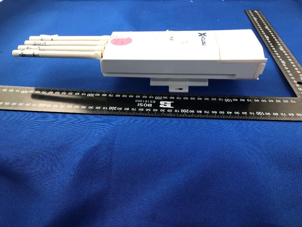
2AMPF-MX1902
Jan 05, 2021MX1902
Equipment Class
DSS - Part 15 Spread Spectrum Transmitter