2AMX5-SC230-V2CARVAAN
Saregama Inc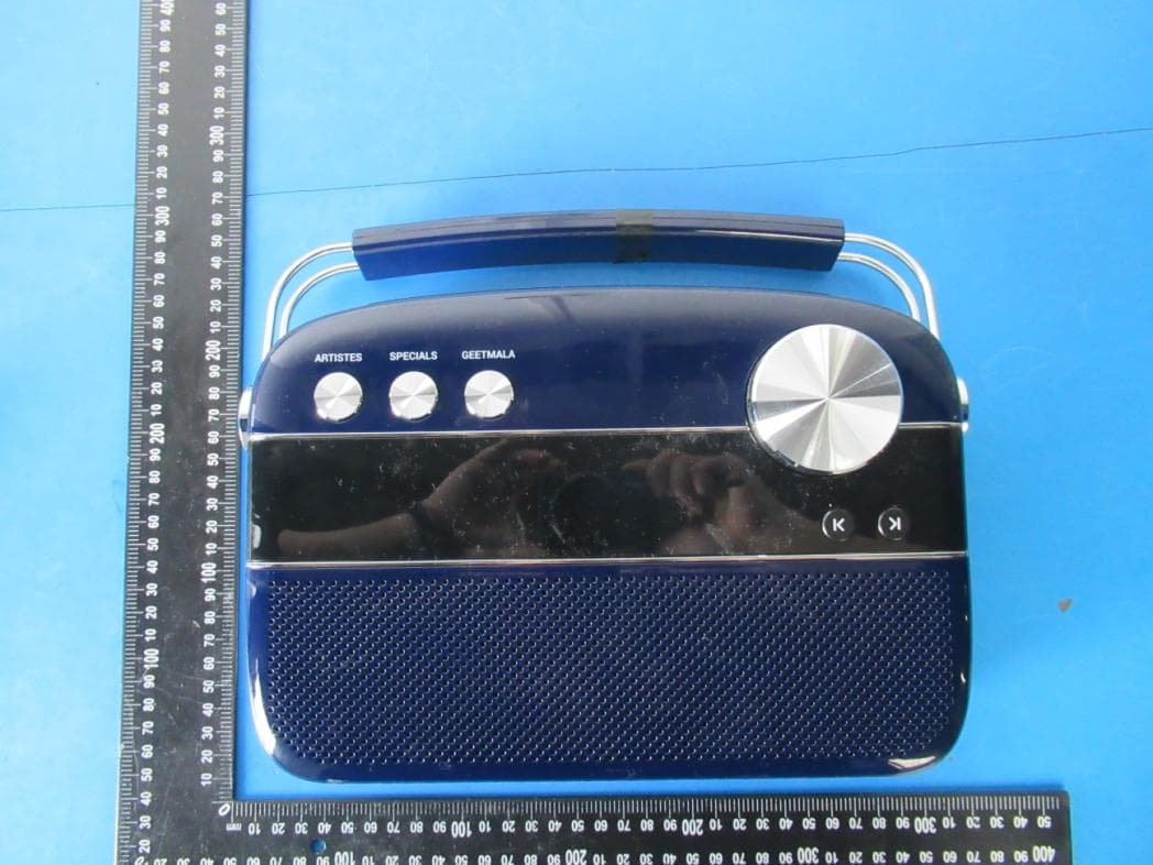
Click to zoom
Application Details
- Equipment Class
- DSS - Part 15 Spread Spectrum Transmitter
- Date of Grant
- Jul 02, 2022
- Application Purpose
- Original Equipment
- Date of Application
- Jul 02, 2022
- Equipment Note
- CARVAAN
- Frequency Range
- 2402.00000000 - 2480.00000000
- Company
- Saregama Inc
- Country
- United States
Documents & Files
Document Text
Text extracted from the exhibit documents filed with the FCC. Open a document above to read the original.
Users Manual
This equipment has been tested and found to comply with the limits for a Class B digital device, pursuant to part 15 of the FCC Rules. These limits are designed to provide reasonable protection against harmful interference in a residential installation. This equipment generates, uses and can radiate radio frequency energy and, if not installed and used in accordance with the instructions, may cause harmful interference to radio communications. However, there is no guarantee that interference will not occur in a particular installation. If this equipment does cause harmful interference to radio or television reception, which can be determined by turning the equipment off and on, the user is encouraged to try to correct the interference by one or more of the following measures: Reorient or relocate the receiving antenna. Increase the separation between the equipment and receiver. Connect the equipment into an outlet on a circuit different from that to which the receiver is connected. Consult the dealer or an experienced radio/TV technician for help. Caution: Any changes or modifications to this device not explicitly approved by manufacturer could void your authority to operate this equipment. This device complies with part 15 of the FCC Rules. Operation is subject to the following two conditions: (1) This device may not cause harmful interference, and (2) this device must accept any interference received, including interference that may cause undesired operation. The device has been evaluated to meet general RF exposure requirement.
Cover Letter(s)
June 29, 2022 Nemko Canada Inc 303 River Road Ottawa, Ontario, Canada K1V 1H2 Attn: Director of Certification Authority to Act as Agent On our behalf, I appoint Shenzhen Alpha Product Testing Co., Ltd. Address: Building i, No.2, Lixin Road, Fuyong Street, Bao’an District, 518103, Shenzhen, Guangdong, China Person: Mark Zhu (Name and address,person). to act as our agent in the preparation of this application for equipment certification. I certify that submitted documents properly describe the device or system for which equipment certification is sought. I also certify that each unit manufactured, imported or marketed, as defined in the Federal Communications Commission’s regulations will have affixed to it a label identical to that submitted for approval with this application. For instances where our authorized agent signs the application for certification on our behalf, I acknowledge that all responsibility for complying with the terms and conditions for certification, as specified by Nemko Canada Inc, still resides with Saregama Inc Address: 200 Continental Drive, Suite 401,Newark, Delaware19713, United States ( applicant name and address). Signature: Name Divyaraj Singh Bisht Position Chief Manager Company Name Saregama Inc Address 200 Continental Drive, Suite 401,Newark, Delaware19713, United States Tel +91981914045 Fax +971 4 817 0201 Email [email protected]
Cover Letter(s)
June 29, 2022 Equipment Autorisation Division Federal Communications Commission 7435 Oakland Mills Road Columbia, MD 21046 FCC ID: 2AMX5-SC230-V2 Product Name: CARVAAN Request for Confidentiality Pursuant to Sections 0.457 and 0.459 of the commissions rules, we hereby request that the following documents be held confidential: Schematics Long-term confidential Block diagram Long-term confidential Operation description Long-term confidential These materials contain trade secrets and proprietary information and are not customarily released to the public. The public disclosure of this information might be harmful to the company and provide unjustified benefits to our competitors. Signature: Name Divyaraj Singh Bisht Position Chief Manager Company Name Saregama Inc Address 200 Continental Drive, Suite 401,Newark, Delaware19713, United States Tel +91981914045 Fax +971 4 817 0201 Email [email protected]
External Photos
FCC ID: 2AMX5-SC230-V2 FCC ID: 2AMX5-SC230-V2 FCC ID: 2AMX5-SC230-V2 FCC ID: 2AMX5-SC230-V2 FCC ID: 2AMX5-SC230-V2
ID Label/Location Info
4.5cm 2.5cm Label Location FCC ID: 2AMX5-SC230-V2 Saregama Inc Product name: CARVAAN Model No.: SC230 This device complies with Part 15 of the FCC Rules. Operation is subject to the following two conditions: (1) this device may not cause harmful interference, and (2) this device must accept any interference received, including interference that may cause undesired operation.
Internal Photos
FCC ID: 2AMX5-SC230-V2 FCC ID: 2AMX5-SC230-V2 FCC ID: 2AMX5-SC230-V2 FCC ID: 2AMX5-SC230-V2 FCC ID: 2AMX5-SC230-V2 FCC ID: 2AMX5-SC230-V2 FCC ID: 2AMX5-SC230-V2 FCC ID: 2AMX5-SC230-V2 FCC ID: 2AMX5-SC230-V2 FCC ID: 2AMX5-SC230-V2 FCC ID: 2AMX5-SC230-V2 FCC ID: 2AMX5-SC230-V2
RF Exposure Info
RF Exposure evaluation According to 447498 D04 Interim General RF Exposure Guidance v01 1-mW Test Exemption A single RF source is exempt RF device (from the requirement to show data demonstrating compliance to RF exposure limits, as previously mentioned) if the available maximum time-averaged power is no more than 1 mW, regardless of separation distance. This exemption applies to all operating configurations and exposure conditions, for the frequency range 100 kHz to 100 GHz, regardless of fixed, mobile, or portable device exposure conditions. This is a standalone exemption, and it cannot be applied in conjunction with any other test exemption. 1-mW Test Exemption for Multiple Sources The 1-mW exemption intended for single transmitters may be also applied to simultaneous transmission conditions, within the same host device, according one of the following criteria: a) When maximum available power each individual transmitting antenna within the same time averaging period is ≤ 1 mW, and the nearest parts of the antenna structures of the simultaneously operating transmitters are separated by at least 2 cm. b) When the aggregate maximum available power of all transmitting antennas is ≤ 1 mW in the same time-averaging period. This exemption may not be combined with any other exemption. SAR-Based Exemption This exemption is applicable to the frequency range between 300 MHz and 6 GHz, with test separation distances between 0.5 cm and 40 cm, and for all RF sources in fixed, mobile, and portable device exposure conditions. Accordingly, a RF source is considered an RF exempt device if its available maximum time-averaged (matched conducted) power or its effective radiated power (ERP), whichever is greater, are below a specified threshold. This exemption threshold was derived based on general population 1-g SAR requirements. This method shall only be used at separation distances from 0.5 cm to 40 cm and at frequencies from 0.3 GHz to 6 GHz (inclusive). Pth is given by follow Formulas “f” is in GHz, “d” is the separation distance (cm) Simultaneous Transmission with SAR-based Exemptions For these cases, a device with multiple RF sources transmitting simultaneously will be considered an RF exempt device if the condition of following Formula is satisfied. (1-mW Test Exemption) As this equipment: Pt = 10 (Pm/10) where: Pt = transmitter output power in milliwatts, Pm = measured transmitter output power in dBm, So Pt =10 (-1.053/10) mW =0.785 mW<1mW Then the SAR test is exempted.
Test Report
ALPHA's reports is using a digital certificate that is trusted on Adobe's official server. If there is no digital certificate or the digital certificate shows damaged in your report. Please do not accept the report. FCC TEST REPORT FCC ID: 2AMX5-SC230-V2 On Behalf of Saregama Inc CARVAAN Model No.: SC230 Prepared for : Saregama Inc Address : 200 Continental Drive, Suite 401,Newark, Delaware19713, United States Prepared By : Shenzhen Alpha Product Testing Co., Ltd. Address : Building i, No.2, Lixin Road, Fuyong Street, Bao’an District, 518103, Shenzhen, Guangdong, China Report Number : A2008280-C01-R02 Date of Receipt : June 21, 2022 Date of Test : June 21, 2022 – June 24, 2022 Date of Report : June 24, 2022 Version Number : V0 Page 2 of 82 Report No.: A2008280-C01-R02 TABLE OF CONTENTS Description Page 1. Summary Of Standards And Results............................................................................................ 6 1.1. Description of Standards and Results ..................................................................................... 6 2. General Information........................................................................................................................ 7 2.1. Description of Device (EUT) .................................................................................................... 7 2.2. Accessories of Device (EUT) .................................................................................................. 8 2.3. Tested Supporting System Details .......................................................................................... 8 2.4. Block Diagram of connection between EUT and simulators ................................................... 8 2.5. Test Mode Description ............................................................................................................. 8 2.6. Test Conditions ........................................................................................................................ 8 2.7. Test Facility .............................................................................................................................. 9 2.8. Measurement Uncertainty ....................................................................................................... 9 2.9. Test Equipment List ............................................................................................................... 10 3. Maximum Peak Output Power ..................................................................................................... 12 3.1. Limit ....................................................................................................................................... 12 3.2. Test Procedure ...................................................................................................................... 12 3.3. Test Setup .............................................................................................................................. 12 3.4. Test Result ............................................................................................................................. 12 4. Bandwidth ..................................................................................................................................... 13 4.1. Limit ....................................................................................................................................... 13 4.2. Test Procedure ...................................................................................................................... 13 4.3. Test Result ............................................................................................................................. 13 5. Carrier Frequency Separation ..................................................................................................... 23 5.1. Limit ....................................................................................................................................... 23 5.2. Test Procedure ...................................................................................................................... 23 5.3. Test Result ............................................................................................................................. 23 6. Number Of Hopping Channel ...................................................................................................... 25 6.1. Limit ....................................................................................................................................... 25 6.2. Test Procedure ...................................................................................................................... 25 6.3. Test Result ............................................................................................................................. 25 7. Dwell Time ..................................................................................................................................... 27 7.1. Test limit ................................................................................................................................. 27 7.2. Test Procedure ...................................................................................................................... 27 7.3. Test Result ............................................................................................................................. 27 8. Radiated Emissions...................................................................................................................... 37 8.1. Limit ....................................................................................................................................... 37 8.2. Block Diagram of Test setup .................................................................................................. 38 8.3. Test Procedure ......................................................................…
Text truncated - open the document above for the full version.
Test Report
Page 59 of 82 Report No.: A2008280-C01-R02 Band Edge(Hopping) NVNT 3-DH1 2402MHz Ant1 Hopping Emission Band Edge NVNT 3-DH1 2402MHz Ant1 No-Hopping Emission Page 60 of 82 Report No.: A2008280-C01-R02 Band Edge(Hopping) NVNT 3-DH1 2480MHz Ant1 Hopping Emission Band Edge NVNT 3-DH1 2480MHz Ant1 No-Hopping Emission Page 61 of 82 Report No.: A2008280-C01-R02 10. Power Line Conducted Emissions 10.1.Block Diagram of Test Setup 10.2.Limit Frequency Maximum RF Line Voltage Quasi-Peak Level dB(V) Average Level dB(V) 150kHz ~ 500kHz 66 ~ 56* 56 ~ 46* 500kHz ~ 5MHz 56 46 5MHz ~ 30MHz 60 50 Notes: 1. * Decreasing linearly with logarithm of frequency. 2. The lower limit shall apply at the transition frequencies. 10.3.Test Procedure (1) The EUT was placed on a non-metallic table, 80cm above the ground plane. (2) Setup the EUT and simulator as shown in 10.1 (3) The EUT Power connected to the power mains through a power adapter and a line impedance stabilization network (L.I.S.N1). The other peripheral devices power cord connected to the power mains through a line impedance stabilization network (L.I.S.N2), this provided a 50-ohm coupling impedance for the EUT (Please refer to the block diagram of the test setup and photographs). Both sides of power line were checked for maximum conducted interference. In order to find the maximum emission, the relative positions of equipments and all of the interface cables were changed according to ANSI C63.10 :2013on conducted Emission test. (4) The bandwidth of test receiver is set at 10KHz. (5) The frequency range from 150 KHz to 30MHz is checked. 10.4.Test Result PASS. (See below detailed test data) Note: If peak Result comply with AV limit, QP and AV Result is deemed to comply with AV limit EUT LISN LISN PC System 80cm Receiver :50 Terminator 0.8m Page 62 of 82 Report No.: A2008280-C01-R02 Pol Line Pol Neutral Remark: All modes have been tested, and only worst data of Charging was listed in this report. Page 63 of 82 Report No.: A2008280-C01-R02 11. Antenna Requirements 11.1.Limit For intentional device, according to FCC 47 CFR Section 15.203, an intentional radiator shall be designed to ensure that no antenna other than that furnished by the responsible party shall be used with the device. And according to FCC 47 CFR Section 15.247 (b), if transmitting antennas of directional gain greater than 6dBi are used, the power shall be reduced by the amount in dB that the directional gain of the antenna exceeds 6dBi. 11.2.Result The EUT antenna is internal antenna. It complies with the standard requirement. Page 64 of 82 Report No.: A2008280-C01-R02 12. Test Setup Photo 12.1.Photos of Radiated emission Page 65 of 82 Report No.: A2008280-C01-R02 12.2.Photos of Power Line Conducted Emission Test Page 66 of 82 Report No.: A2008280-C01-R02 13. Photos Of EUT Page 67 of 82 Report No.: A2008280-C01-R02 Page 68 of 82 Report No.: A2008280-C01-R02 Page 69 of 82 Report No.: A2008280-C01-R02 Page 70 of 82 Report No.: A2008280-C01-R02 Page 71 of 82 Report No.: A2008280-C01-R02 Page 72 of 82 Report No.: A2008280-C01-R02 Page 73 of 82 Report No.: A2008280-C01-R02 Page 74 of 82 Report No.: A2008280-C01-R02 Page 75 of 82 Report No.: A2008280-C01-R02 Page 76 of 82 Report No.: A2008280-C01-R02 Page 77 of 82 Report No.: A2008280-C01-R02 Page 78 of 82 Report No.: A2008280-C01-R02 Page 79 of 82 Report No.: A2008280-C01-R02 Page 80 of 82 Report No.: A2008280-C01-R02 Page 81 of 82 Report No.: A2008280-C01-R02 Page 82 of 82 Report No.: A2008280-C01-R02 ---------THE END OF REPORT-------
Test Setup Photos
FCC ID: 2AMX5-SC230-V2 Radiated Emission FCC ID: 2AMX5-SC230-V2 Conducted Emission
Contact Information
Applicant
Divyaraj Singh Bisht(Chief Manager)
Test Firm
Shenzhen Alpha Product Testing Co., LTD.Real Yak
[email protected]+86 755 29766001
Technical Specifications
| # | Rule Parts | Frequency Range | Power Output |
|---|---|---|---|
| 1 | 15C | 2.40 GHz - 2.48 GHz | 780.00 µW |
Other Applications from Saregama Inc
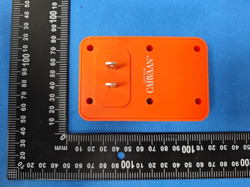
2AMX5-SCPP130
Aug 07, 2024CARVAAN Plug play
Equipment Class
DSS - Part 15 Spread Spectrum Transmitter
2AMX5-SSCKM130
Jan 04, 2024CARVAAN Mini
Equipment Class
DSS - Part 15 Spread Spectrum Transmitter
2AMX5-MSCKM130
Jan 01, 2024CARVAAN Mini
Equipment Class
DSS - Part 15 Spread Spectrum Transmitter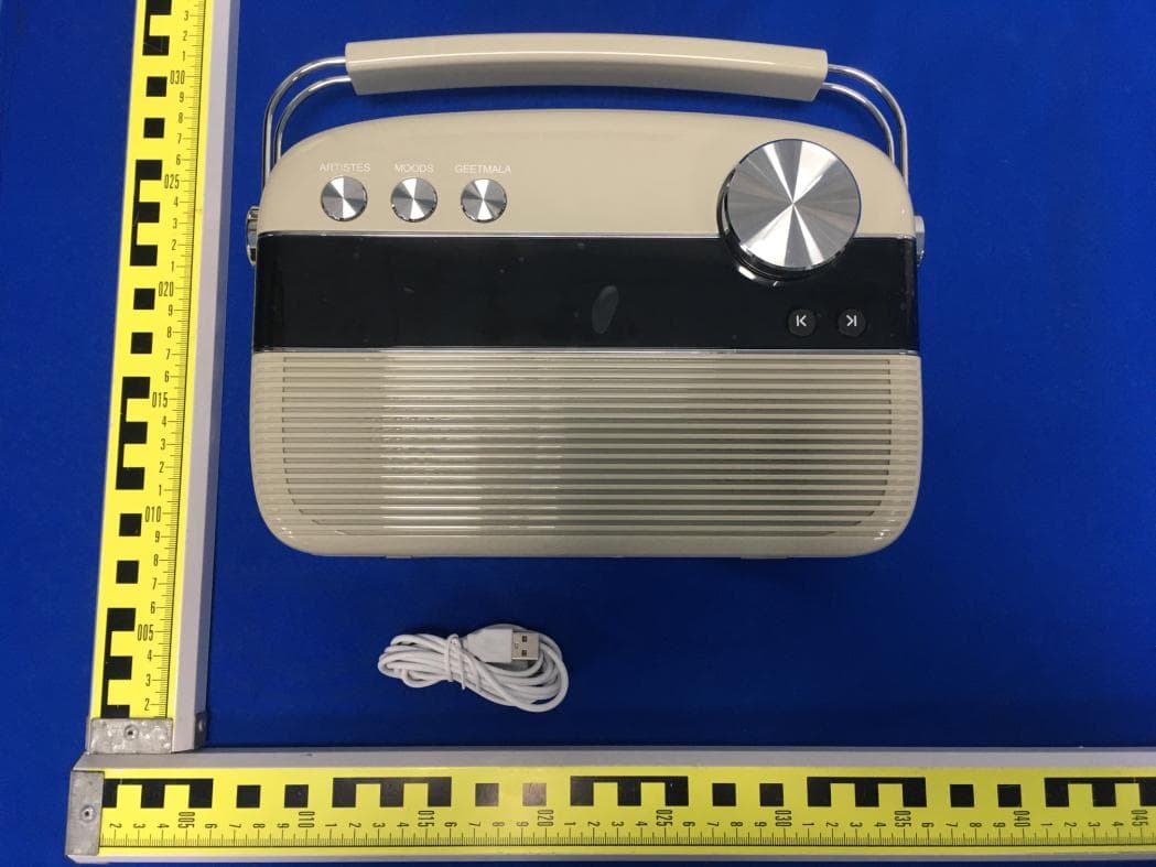
2AMX5-SC03-V2
Jul 02, 2022CARVAAN
Equipment Class
DSS - Part 15 Spread Spectrum Transmitter