2AOFNCBC003VIBRANT WIRELESS EARBUDS
iWorld Global Trading LLC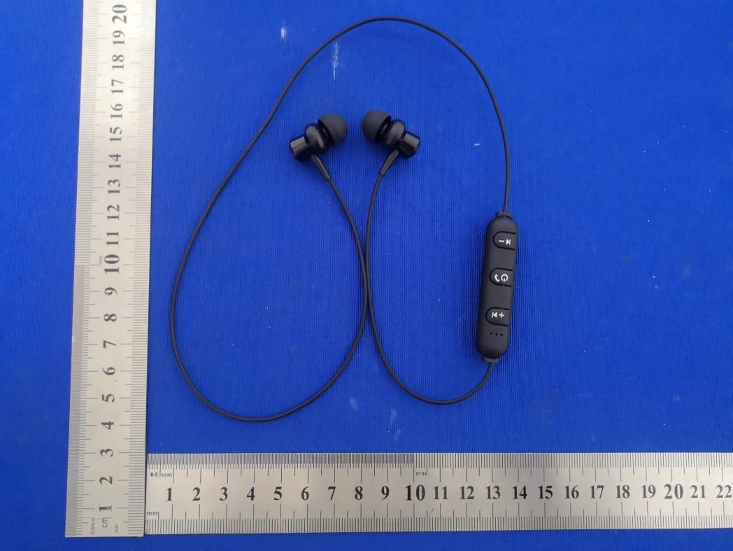
Click to zoom
Application Details
- Equipment Class
- DSS - Part 15 Spread Spectrum Transmitter
- Date of Grant
- Nov 24, 2020
- Application Purpose
- Original Equipment
- Date of Application
- Nov 24, 2020
- Equipment Note
- VIBRANT WIRELESS EARBUDS
- Frequency Range
- 2402.00000000 - 2480.00000000
- Company
- iWorld Global Trading LLC
- Country
- United States
Documents & Files
Document Text
Text extracted from the exhibit documents filed with the FCC. Open a document above to read the original.
Cover Letter(s)
(iWorld Global Trading LLC) Federal Communications Commission Authorization and Evaluation Division Confidentiality Request regarding application for certification of FCC ID: 2AOFNCBC003 Pursuant to Sections 0.457 and 0.459 of the Commission’s Rules, we hereby request confidential treatment of information accompanying this application as outlined below: Exhibit Type File Name Block Diagram, Schematics, Operational Description Block Diagram Schematics Operational Description The above materials contain trade secrets and proprietary information not customarily released to the public. The public disclosure of these materials may be harmful to the applicant and provide unjustified benefits to its competitors. The applicant understands that pursuant to Section 0.457 of the Rules, disclosure of this application and all accompanying documentation will not be made before the date of the Grant for this application. Sincerely, ( Yafit Shahar) Rev 11/20/07
Cover Letter(s)
(iWorld Global Trading LLC) Federal Communications Commission Authorization and Evaluation Division 1435 Oakland Mills Road Columbia, MD 21046 Date: SUBJECT: FCC Application for FCC ID: 2AOFNCBC003 To Whom It May Concern: We, the undersigned, hereby authorize Alan Mei at Shenzhen BCTC Testing Co., Ltd. on our behalf, to apply to the Federal Communications Commission on our equipment. Any and all acts carried out by Alan Mei of Shenzhen BCTC Testing Co., Ltd. on our behalf shall have the same effect as acts of our own. This is to advise that we are in full compliance with the Anti- Drug Abuse Act. We, the applicant, are not subject to a denial of federal benefits pursuant to Section 5301 of the Anti-Drug Act of 1988, 21 USC853a, and no party to the application is subject to a denial of federal benefits pursuant to that section. Regards, ( Yafit Shahar)
External Photos
Ex ternal Photos
ID Label/Location Info
Label & label location Model:WI8BT-1000-BK FCC ID:2AOFNCBC003
Internal Photos
Internal Photos Antenna
RF Exposure Info
RF EXPOSURE EVALUATION METHOD FCC ID: 2AOFNCBC003 SAR Test Exclusion Thresholds for 100 MHz – 6 GHz and ≤ 50 mm Approximate SAR Test Exclusion Power Thresholds at Selected Frequencies and Test Separation Distances are illustrated in the following Table. The 1-g and 10-g SAR test exclusion thresholds for 100 MHz to 6 GHz at test separation distances ≤ 50 mm are determined by: [(max. power of channel, including tune-up tolerance, mW)/(min. test separation distance, mm)] · [√f(GHz)] ≤ 3.0 for 1-g SAR and ≤ 7.5 for 10-g extremity SAR,where f(GHz) is the RF channel transmit frequency in GHz Power and distance are rounded to the nearest mW and mm before calculation The result is rounded to one decimal place for comparison The test exclusions are applicable only when the minimum test separation distance is ≤ 50 mm and for transmission frequencies between 100 MHz and 6 GHz. When the minimum test separation distance is < 5 mm, a distance of 5 mm is applied to determine SAR test exclusion. BT-EDR max possible output power (PK,conducted):-2±1dBm -0.58dBi logarithmic terms convert to numeric result is nearly 0.875 -1dbm=0.79mW Modulation Frequency (MHz) Output Power (dBm) Max Antenna Gain (dBi) GFSK 2402 -4.405 -0.58 GFSK 2441 -3.679 -0.58 GFSK 2480 -3.793 -0.58 Pi/4 DQPSK 2402 -3.193 -0.58 Pi/4 DQPSK 2441 -2.499 -0.58 Pi/4 DQPSK 2480 -2.564 -0.58 EDR: 2402MHz [(max. power of channel, including tune-up tolerance, mW)/(min. test separation distance,mm)] · [√f(GHz)]=0.79/5*√2.402 =0.24≤3.0 Threshold at which no SAR required is 10mw and ≤ 3.0 for 1-g SAR, Separation distance is 5mm. 2441 MHz [(max. power of channel, including tune-up tolerance, mW)/(min. test separation distance,mm)] · [√f(GHz)]= 0.79/5*√2.441 =0.25≤3.0 Threshold at which no SAR required is 10mw and ≤ 3.0 for 1-g SAR, Separation distance is 5mm. 2480MHz [(max. power of channel, including tune-up tolerance, mW)/(min. test separation distance,mm)] · [√f(GHz)]=0.79/5*√2.48=0.25≤3.0 Threshold at which no SAR required is 10mw and ≤ 3.0 for 1-g SAR, Separation distance is 5mm. Conclusion: No SAR is required.
Test Report
No.:BCTC/RF-EMC-005 Page: 1 of 60 Edition:A.2 TEST REPORT Shenzhen BCTC Testing Co., Ltd. Report No.: BCTC2011001191E Applicant: iWorld Global Trading LLC Product Name: VIBRANT WIRELESS EARBUDS Model/Type Ref.: WI8BT-1000-BK Tested Date: Nov. 16, 2020 to Nov. 20, 2020 Issued Date: Nov. 2 3, 2020 Report No.: BCTC2011001191E No.:BCTC/RF-EMC-005 Page: 2 of 60 Edition:A.2 FCC ID :2AOFNCBC003 The test report is effective only with both signature and specialized stamp.This result(s) shown in this report refer only to the sample(s) tested. Without written approval of Shenzhen BCTC Testing Co., Ltd, this report can’t be reproduced except in full.The tested sample(s) and the sample information are provided by the client. Product Name: VIBRANT WIRELESS EARBUDS Trademark: N/A Model/Type Ref.: WI8BT-1000-BK WI8BT-1000-RD Prepared For: iWorld Global Trading LLC Address: 65 West 36th Street 11th floor, NY 10018, United States Manufacturer: Dongguan meiyin technology co., ltd. Address: Building C, No. 1, Zhiquan hi-tech park road, Dongkeng town, Dongguan city, China Prepared By: Shenzhen BCTC Testing Co., Ltd. Address: 1-2F, East of B Building, Pengzhou Industrial, Fuyuan 1st Road, Qiaotou Community, Fuyong Street, Bao’an District, Shenzhen, China Sample Received Date: Nov. 16, 2020 Sample tested Date: Nov. 16, 2020 to Nov. 20, 2020 Issue Date: Nov. 23, 2020 Report No.: BCTC2011001191E Test Standards FCC Part15.247 ANSI C63.10-2013 Test Results PASS Remark: This is Bluetooth Classic radio test report. Tested by: Approved by: Cathy Zhong/ Project Handler Zero Zhou/Reviewer Report No.: BCTC2011001191E No.:BCTC/RF-EMC-005 Page: 3 of 60 Edition:A.2 TABLE OF CONTENT Test Report Declaration Page 1. VERSION ............................................................ 5 2. TEST SUMMARY ..................................................... 6 3. MEASUREMENT UNCERTAINTY ....................................... 7 4. PRODUCT INFORMATION AND TEST SETUP ........................... 8 4.1 Product Information ..................................................... 8 4.2 Test Setup Configuration ................................................ 8 4.3 Support Equipment ..................................................... 9 4.4 Channel List ........................................................... 9 4.5 Test Mode ............................................................ 10 4.6 table of parameters of text software setting ................................ 10 5. TEST FACILITY AND TEST INSTRUMENT USED ........................ 11 5.1 Test Facility ........................................................... 11 5.2 Test Instrument Used .................................................. 11 6. CONDUCTED EMISSIONS ............................................ 13 6.1 Block Diagram Of Test Setup ........................................... 13 6.2 Limit ................................................................. 13 6.3 Test procedure ........................................................ 13 6.4 EUT operating Conditions .............................................. 13 6.5 Test Result ........................................................... 14 7. RADIATED EMISSIONS .............................................. 16 7.1 Block Diagram Of Test Setup ........................................... 16 7.2 Limit ................................................................. 17 7.3 Test procedure ........................................................ 18 7.4 EUT operating Conditions .............................................. 19 7.5 Test Result ........................................................... 20 8. RADIATED BAND EMISSION MEASUREMENT AND RESTRICTED BANDS OF OPERATION .......................................................... 24 8.1 Block Diagram Of Test Setup ........................................... 24 8.2 Limit ................................................................. 24 8.3 Test procedure ........................................................ 25 8.4 EUT operating Conditions .............................................. 25 8.5 Test Result ........................................................... 26 9. CONDUCTED EMISSION ............................................. 27 9.1 Block Diagram Of Test Setup ........................................... 27 9.2 Limit ................................................................. 27 9.3 Test procedure ........................................................ 27 9.4 Test Result ........................................................... 28 10. 20 DB BANDWIDTH .................................................. 34 10.1 Block Diagram Of Test Setup .......................................... 34 10.2 Limit ................................................................ 34 10.3 Test procedure ....................................................... 34 10.4 Test Result .......................................................... 35 Report No.: BCTC2011001191E No.:BCTC/RF-EMC-005 Page: 4 of 60 Edition:A.2 11. MAXIMUM PEAK OUTPUT POWER .................................... 39 11.1 Block Diagram Of Test Setup .......................................... 39 11.2 Limit ................................................................ 39 11.3 Test procedure ....................................................... 39 11.4 Test Result .......................................................... 40 12. HOPPING CHANNEL SEPARATION ................................... 44 12.1 Block Diagram Of Test Setup .......................................... 44 12.2 Limit ................................................................ 44 12.3 Test procedure ....................................................... 44 12.4 Test Result .......................................................... 45 13. NUMBER OF HOPPING FREQUENCY .................................. 49 13.1 Block Diagram Of Test Setup .......................................... 49 13.2 Limit ..........................................................…
Text truncated - open the document above for the full version.
Test Report
Report No.: BCTC2011001191E No.:BCTC/RF-EMC-005 Page: 28 of 60 Edition:A.2 9. 4 Test Result Temperature: 26°C Relative Humidity: 54% Test Voltage : DC 3.7V Remark: N/A 30MHz – 25GHz GFSK Low Channel GFSK Middle Channel GFSK High Channel Report No.: BCTC2011001191E No.:BCTC/RF-EMC-005 Page: 29 of 60 Edition:A.2 Pi/4 DQPSK Low Channel Pi/4 DQPSK Middle Channel Pi/4 DQPSK High Channel Report No.: BCTC2011001191E No.:BCTC/RF-EMC-005 Page: 30 of 60 Edition:A.2 GFSK Transmitting Band edge-left side GFSK Hopping Band edge-left side Report No.: BCTC2011001191E No.:BCTC/RF-EMC-005 Page: 31 of 60 Edition:A.2 GFSK Transmitting Band edge-right side GFSK Hopping Band edge-right side Report No.: BCTC2011001191E No.:BCTC/RF-EMC-005 Page: 32 of 60 Edition:A.2 Pi/4 DQPSK Transmitting Band edge-left side Pi/4 DQPSK Hopping Band edge-left side Report No.: BCTC2011001191E No.:BCTC/RF-EMC-005 Page: 33 of 60 Edition:A.2 Pi/4 DQPSK Transmitting Band edge-right side Pi/4 DQPSK Hopping Band edge-right side Report No.: BCTC2011001191E No.:BCTC/RF-EMC-005 Page: 34 of 60 Edition:A.2 10. 20 DB BANDWIDTH 10.1 Block Diagram Of Test Setup 10.2 Limit N/A 10.3 Test procedure 1. Set RBW = 30kHz. 2. Set the video bandwidth (VBW) ≥ 3 x RBW. 3. Detector = Peak. 4. Trace mode = max hold. 5. Sweep = auto couple. 6. Allow the trace to stabilize. 7. Measure the maximum width of the emission that is constrained by the frequencies associated with the two outermost amplitude points (upper and lower frequencies) that are attenuated by 6 dB relative to the maximum level measured in the fundamental emission. . Report No.: BCTC2011001191E No.:BCTC/RF-EMC-005 Page: 35 of 60 Edition:A.2 10.4 Test Result Temperature: 26°C Relative Humidity: 54% Test Voltage : DC 3.7V Remark N/A Modulation Test Channel Bandwidth(MHz) GFSK Low 0.840 GFSK Middle 0.837 GFSK High 0.843 Pi/4 DQPSK Low 1.213 Pi/4 DQPSK Middle 1.216 Pi/4 DQPSK High 1.210 Report No.: BCTC2011001191E No.:BCTC/RF-EMC-005 Page: 36 of 60 Edition:A.2 Test plots GFSK Low Channel GFSK Middle Channel Report No.: BCTC2011001191E No.:BCTC/RF-EMC-005 Page: 37 of 60 Edition:A.2 GFSK High Channel Pi/4 DQPSK Low Channel Report No.: BCTC2011001191E No.:BCTC/RF-EMC-005 Page: 38 of 60 Edition:A.2 Pi/4 DQPSK Middle Channel Pi/4 DQPSK High Channel Report No.: BCTC2011001191E No.:BCTC/RF-EMC-005 Page: 39 of 60 Edition:A.2 11. MAXIMUM PEAK OUTPUT POWER 11.1 Block Diagram Of Test Setup 11.2 Limit FCC Part15 (15.247) , Subpart C Section Test Item Limit Frequency Range (MHz) Result 15.247(b)(1) Peak Output Power 0.125 watt or 21dBm 2400-2483.5 PASS 11.3 Test procedure 1. Remove the antenna from the EUT and then connect a low RF cable from the antenna port to the spectrum. 2. Set the spectrum analyzer: RBW = 3MHz. VBW = 3MHz. Sweep = auto; Detector Function = Peak. 3. Keep the EUT in transmitting at lowest, medium and highest channel individually. Record the max value. Report No.: BCTC2011001191E No.:BCTC/RF-EMC-005 Page: 40 of 60 Edition:A.2 11.4 Test Result Temperature: 26°C Relative Humidity: 54% Test Voltage : DC 3.7V Remark: N/A Modulation Test Channel Output Power (dBm) Limit (dBm) GFSK Low -4.405 21 GFSK Middle -3.679 21 GFSK High -3.793 21 Pi/4 DQPSK Low -3.193 21 Pi/4 DQPSK Middle -2.499 21 Pi/4 DQPSK High -2.564 21 Report No.: BCTC2011001191E No.:BCTC/RF-EMC-005 Page: 41 of 60 Edition:A.2 Test plots GFSK Low Channel GFSK Middle Channel Report No.: BCTC2011001191E No.:BCTC/RF-EMC-005 Page: 42 of 60 Edition:A.2 GFSK High Channel Pi/4 DQPSK Low Channel Report No.: BCTC2011001191E No.:BCTC/RF-EMC-005 Page: 43 of 60 Edition:A.2 Pi/4 DQPSK Middle Channel Pi/4 DQPSK High Channel Report No.: BCTC2011001191E No.:BCTC/RF-EMC-005 Page: 44 of 60 Edition:A.2 12. HOPPING CHANNEL SEPARATION 12.1 Block Diagram Of Test Setup 12.2 Limit Frequency hopping systems shall have hopping channel carrier frequencies separated by a minimum of 25 kHz or the 20 dB bandwidth of the hopping channel, whichever is greater. Alternatively, frequency hopping systems operating in the 2400-2483.5 MHz band may have hopping channel carrier frequencies that are separated by 25 kHz or two-thirds of the 20 dB bandwidth of the hopping channel, whichever is greater, provided the systems operate with an output power no greater than 0.125W. 12.3 Test procedure 1. Remove the antenna from the EUT and then connect a low RF cable from the antenna port to the spectrum. 2. Set the spectrum analyzer: RBW = 30kHz. VBW = 100kHz , Span = 2.0MHz. Sweep = auto; Detector Function = Peak. Trace = Max hold. 3. Allow the trace to stabilize. Use the marker-delta function to determine the separation between the peaks of the adjacent channels. The limit is specified in one of the subparagraphs of this Section Submit this plot. Report No.: BCTC2011001191E No.:BCTC/RF-EMC-005 Page: 45 of 60 Edition:A.2 12.4 Test Result Modulation Test Channel Separation (MHz) Limit(MHz) Result GFSK Low 0.998 0.560 PASS GFSK Middle 1.008 0.558 PASS GFSK High 1.010 0.562 PASS Pi/4 DQPSK Low 1.002 0.809 PASS Pi/4 DQPSK Middle 0.998 0.811 PASS Pi/4 DQPSK High 1.000 0.807 PASS Report No.: BCTC2011001191E No.:BCTC/RF-EMC-005 Page: 46 of 60 Edition:A.2 Test plots GFSK Low Channel GFSK Middle Channel Report No.: BCTC2011001191E No.:BCTC/RF-EMC-005 Page: 47 of 60 Edition:A.2 GFSK High Channel Pi/4 DQPSK Low Channel Report No.: BCTC2011001191E No.:BCTC/RF-EMC-005 Page: 48 of 60 Edition:A.2 Pi/4 DQPSK Middle Channel Pi/4 DQPSK High Channel Report No.: BCTC2011001191E No.:BCTC/RF-EMC-005 Page: 49 of 60 Edition:A.2 13. NUMBER OF HOPPING FREQUENCY 13.1 Block Diagram Of Test Setup 13.2 Limit Frequency hopping systems in the 2400-2483.5 MHz band shall use at least 15 channels. 13.3 Test procedure 1. Remove the antenna from the EUT and then connect a low RF cable from the antenna port to the spectrum. 2. Set the spectrum analyzer: RBW = 100kHz. VBW = 300kHz. Sweep = auto; Detector Function = Peak. Trace = Max hold. 3. Allow the trace to stabilize. It may prove necessary to break the span up to s…
Text truncated - open the document above for the full version.
Test Setup Photos
1. EUT TEST SETUP PHOTOGRAPHS Conducted emissions Radiated Measurement Photos
Contact Information
Applicant
Yafit Shahar
Test Firm
Shenzhen BCTC Testing Co., Ltd.Sally He
[email protected]15999690624
Technical Specifications
| # | Rule Parts | Frequency Range | Power Output |
|---|---|---|---|
| 1 | 15C | 2.40 GHz - 2.48 GHz | 1.00 mW |
Other Applications from iWorld Global Trading LLC
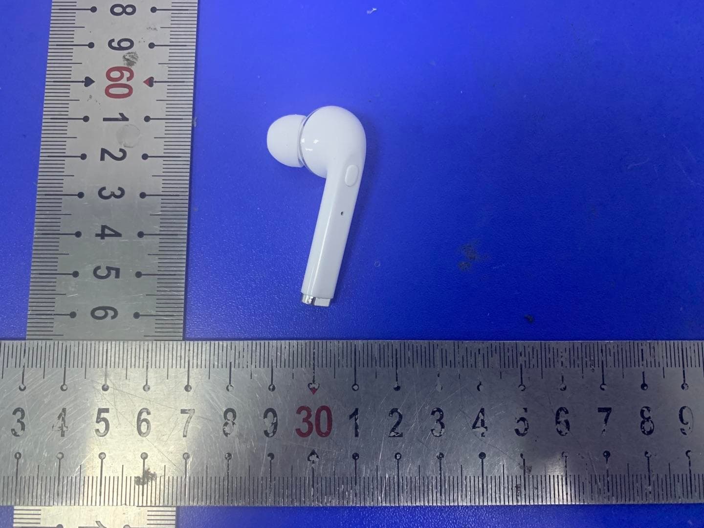
2AOFN-PATW-1005
Oct 13, 2020VAPOR TRUE WIRELESS EARBUDS
Equipment Class
DTS - Digital Transmission System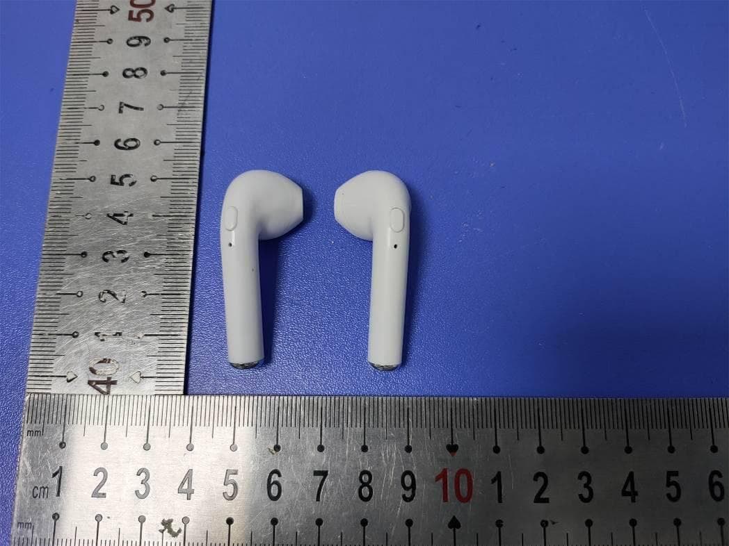
2AOFNCBC002
May 26, 2020True Wireless Earbuds
Equipment Class
DTS - Digital Transmission System