2AV9TDS-52810-03BLE
SHENZHEN DEASINO TECHNOLOGY CO ., LTD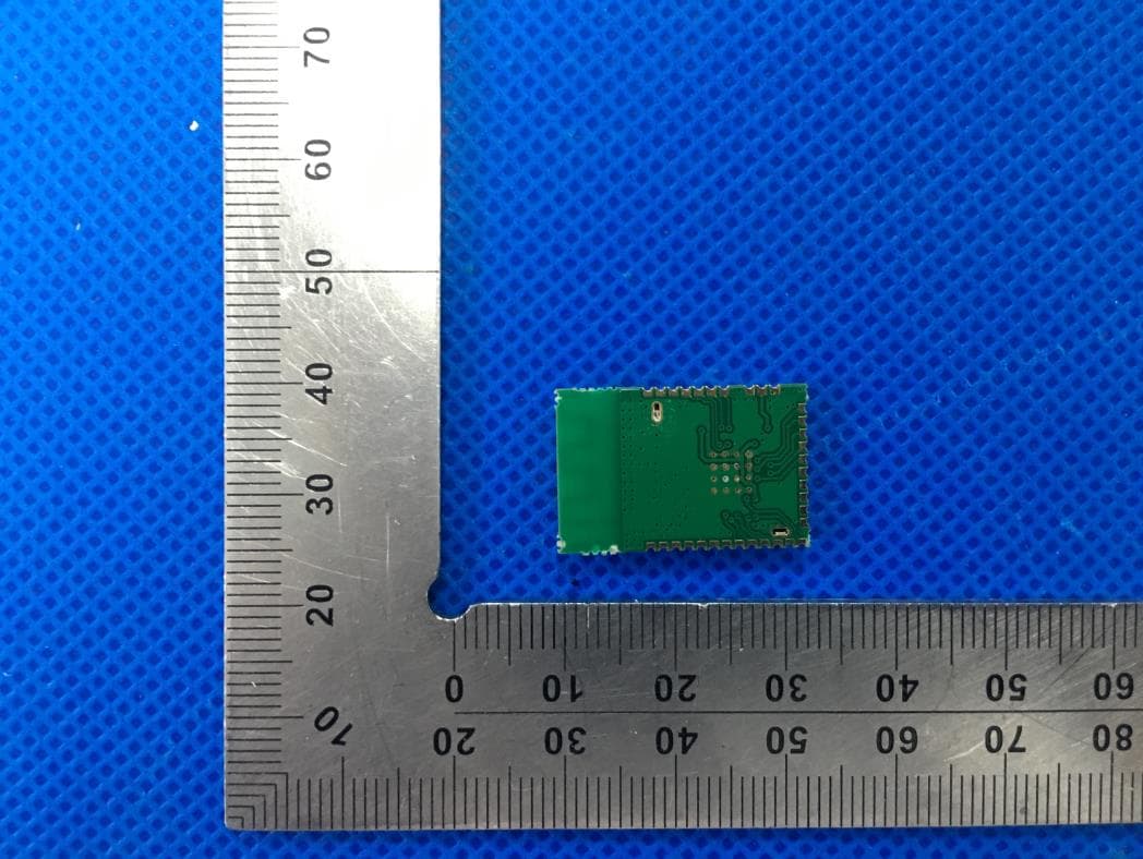
Click to zoom
Application Details
- Equipment Class
- DTS - Digital Transmission System
- Date of Grant
- Jun 28, 2020
- Application Purpose
- Original Equipment
- Date of Application
- Jun 28, 2020
- Equipment Note
- BLE
- Frequency Range
- 2402.00000000 - 2480.00000000
- Country
- China
Documents & Files
Document Text
Text extracted from the exhibit documents filed with the FCC. Open a document above to read the original.
Users Manual
Page 1 of 15 DEASINO DS-52810-03 Datasheet Version:V1.0.0 SHEZHEN DEASINO TECHNOLOGY.,LTD Property in copyright Page 2 of 15 DEASINO VERSION HISTORY REVISION AMENDMENT DATA Page 3 of 15 DEASINO DESCRIPTION DS-52810-03 is an external antenna Bluetooth low power module. DS-52810-03 integrates all features of Bluetooth radio,software stack,GATT based profiles,antenna and host end user applications,which means no external micro controller. It provides a Bluetooth Low Energy fully compliant system for a data communication. At +4 dBm TX Power and -93dBm RX Sensitivity DS-52810-03 has best RF performance. APPLICATIONFEATURE -Commercial - Bluetooth v5.0 Single Mode Compliant -Sports and fitness - Integrated Bluetooth Smart Stack -Healthcare .GAP, GATT,L2CAP and SMP -Medical sensors .Bluetooth Smart profiles -Home entertainment - RF Performance - Watch .Transmit power:+4dBm(-20 dBm to +4 dBm) - Human interface devices .Receiver sensitivity:-96 dBm - Low Power Consumption .Transmit:7.5 mA peak .Receiver:12.9 mA peak .Sleep mode:0.5uA - Peripheral Interfaces .UART/SPI(Master/Slave)/I2C .GPIO .12-bit ADC .I2S and PDM .Temperature Sensor - Power supply:1.7 to 3.6V - Dimension:14.8x22.7x1.7 mm(W x L x H) <Figure 1.DS-52810-03> Page 4 of 15 DEASINO 1.Block Diagram DS-52810-03 block diagram is illustrated in figure 2 below. <Figure 2.Simplified block diagram of DS-52810-03> Page 5 of 15 DEASINO CPU and Memory The Main core is ARM Cortex-M4.The processor implements several features that enable energy-efficient arithmetic and high-performance signal processing including”digital signal processing” ,”Single-cycle multiply and accumulate instructions”, ”hardware divide”, “8 and 16-bit single instruction multiple data instructions” and “ Single-precision floating-point unit” The ARM Cortex Microcontroller Software Interface Standard (CMSIS) hardware abstraction layer for the ARM Cortex processor series is implemented and available for the M4 CPU. Real-time execution is highly deterministic in thread mode, to and from sleep modes, and when handing events at configurable priority levels via the Nested Vectored Interrupt Controller(NVIC). The floating point unit (FPU) may generate exceptions when sed due to e.g. overflow or underflow. These exceptions will trigger the FPU interrupt. The 24-KB SRAMof 1024 byte page size and 192-KB flashof 8-KB block size memory are provided Power management DS-52810-03supporttwodifferentpowersupplyalternativesof Internal LDO mode and Low voltage mode. In internal LDO mode, the system power is generated directly from the supply voltage VDD. In low voltage mode, the system power is supplied by 1.8V. The module’s power management features are System OFF mode and System ON mode. In system OFF mode, the module is in deepest power saving mode. The system’s core functionality is powered down and all ongoing tasks are terminated. In system ON mode, the module is fully operational and CPU and selected peripherals can be brought into a state where they are functional and more or less responsive depending on the sub-power mode selected by Low power or Constant latency. Clock management The module has a 32MHz main crystal oscillator and 32.768kHz RTC crystal oscillator. Peripherals Page 6 of 15 DEASINO The general GPIO is organized as one port with up to 33 I/Os enabling access and control of up to 28 pins through one port. Each GPIO can be accessed individually with the following user configurable features. - Input/output direction - Output drive strength - Internal pull-up and pull-down resistors - Wake-up from high or low level triggers on all pins - Trigger interrupt on all pins - All pins can be used by the PPI task/event system. The maximum number of pins that canbe interfaced through the PPI at the same time is limited by the number of GPIOTEchannels - All pins can be individually configured to carry serial interface orquadrature demodulator signals. The transceiver receives and transmits data directly to and from system memory for flexible andefficient packet data management. The module's transceiver has the following features. - General modulation features .GFSK modulation .Data whitening .On-air data rates(250 kbps/1 Mbps/2 Mbps) - Transmitter with programmable output power of +4 dBm to-20 dBm, in 4 dB step - RSSI function(1 dB resolution) - Receiver with integrated channel filters achieving maximum sensitivity - Baseband controller .EasyDMA RX and TX packet transfer directly to and from RAM .Dynamic payload length .On-the-fly packet assembly/disassembly and AES CCM payload encryption . 8 bit, 16 bit and 24 bit CRC check The timer runs on the high-frequency clock source(HFCLK) and includes a four-bit (1/2X)prescaler that can divide the timer input clock from the HFCLK controller Clock source selectionbetween PCLK16M and PCLKlM is automatic according to timer base frequency set by the prescaler. The timer base frequency is always given as 16 MHz divided by the prescaler value. The PPI system allows a TIMER event to trigger a task of any other system peripheral ofdevice. The PPI system also enables the TIMER task/event features to generate periodic outputand PWM signals to any GPIO. The number of input/outputs used at the same time is limited bythe number of GPIOTE channels. Page 7 of 15 DEASINO The temperature sensor measures die temperature over the temperature range of the device with0. 25 degree resolution. The SPI is implemented with Easy DMA support for ultra low power serial communication from anexternal SPI master. Easy DMA in conjunction with hardware-based semaphore mechanismsremoves all real-time requirements associated with controlling the SPI slave from a low priority CPU execution context. The TWI slave with EasyDMA(TWIS) is compatible with I2C operating at 100 kHz and 400 kHz.The TWI transmitter and receiver implement Easy DMA. The Universal asynchronous receiver/transmitter with Easy DMA (UART) offers fast, full-duplex,asynchronous serial communication with built-in f…
Text truncated - open the document above for the full version.
Cover Letter(s)
SHENZHEN DEASINO TECHNOLOGY CO .,LTD Modular Approval Request Letter Date: 2020-06-30 FCC ID: 2AV9TDS-52810-03 Type of Equipment: Single Module The following requirements according to FCC Part 15.212 are met: i RF shielding The radio portion has his own shielding (see external photos). ii Buffered modulation/data inputs, has been integrated in the chipset iii Power supply regulation, is integrated iv Antenna requirements section 15.203, 15.204 b and 15.204 c The module comes with one permanently attached antennas. The spurious emission requirements are fulfilled (see attached test report). v Stand alone test configuration Please referring to test set up configuration photo vi Labelling The module has its own label. The instruction for labelling rules for the host device has been stated in the users manual vii Compliance on specific rule or operating requirements The required FCC rules has been fulfilled and all instructions for maintaining compliance has been clearly stated in the users manual viii RF Exposure, RF exposure requirements are fulfilled for mobile configuration. The installation of the module is restricted to mobile host devices what is clearly stated in the installation instruction of the user manual. For portable applications OEM integrators need SAR evaluation and an own FCC ID. Tiger tan Manager SHENZHEN DEASINO TECHNOLOGY CO ., LTD
External Photos
External Photos TOP VIEW OF EUT BOTTOM VIEW OF EUT FRONT VIEW OF EUT BACK VIEW OF EUT LEFT VIEW OF EUT RIGHT VIEW OF EUT
ID Label/Location Info
FCC ID Label Location FCC ID: 2AV9TDS-52810-03
Internal Photos
Internal Photos VIEW OF EUT (open) INTERNAL VIEW OF EUT-1 Antenna
Operational Description
SHENZHEN DEASINO TECHNOLOGY CO .,LTD Declaration concerning Antenna Specification It is hereby declared that the product Model No.: DS-52810-03 FCC ID: 2AV9TDS-52810-03 fulfills the requirement in FCC test relating to the antenna type. The device specified above confirms to the FCC recommendations for internal antenna type(s) described below: Type of antenna: PCB Antenna Gain of the antenna: 0 dBi Frequency range: 2.402 GHz to 2.480GHz The mounting of the antenna is fixed to the radio module and no other antenna should be used. Company name: SHENZHEN DEASINO TECHNOLOGY CO ., LTD Address: Floor 3B, 4Building, YongQi Technology Park, YinTian Industrial Zone, XiXiang, Baoan District Shenzhen Place: Shenzhen Date: 2020-06-02 Signature:
RF Exposure Info
RF EXPOSURE EVALUATION 1. PRODUCT INFORMATION Product Description BLE Model Name DS-52810-03 FCC ID 2AV9TDS-52810-03 2. EVALUATION METHOD According to 447498 D01 General RF Exposure Guidance v05 The 1-g and 10-g SAR test exclusion thresholds for 100 MHz to 6 GHz at test separation distances ≤ 50 mm are determined by: [(max. power of channel, including tune-up tolerance, mW)/(min. test separation distance, mm)] ·[√f(GHz)] ≤ 3.0 for 1-g SAR and ≤ 7.5 for 10-g extremity SAR. Where f(GHz) is the RF channel transmit frequency in GHz Power and distance are rounded to the nearest mW and mm before calculation 3. CALCULATION GFSK-1M Pt=-3.913dBm=0.41mW The value of the Maximum output power P t is referred to the test report of the CFR47 §15.247. The result for RF exposure evaluation SAR=(0.41mW /5mm) .[√2.480(GHz)]= 0.13<3.0 for 1-g SAR and ≤ 7.5 for 10-g extremity SAR. GFSK-2M P t =-3.984dBm=0.40mW The value of the Maximum output power P t is referred to the test report of the CFR47 §15.247. The result for RF exposure evaluation SAR=(0.40mW /5mm) .[√2.480(GHz)]= 0.13<3.0 for 1-g SAR and ≤ 7.5 for 10-g extremity SAR. 4. CONCLUSION The SAR evaluation is not required.
Test Report
Page 1 of 46 FCC Test Report Report No.: AGC07581200405FE02 FCC ID : 2AV9TDS-52810-03 APPLICATION PURPOSE : Original Equipment PRODUCT DESIGNATION : BLE BRAND NAME : DEASINO MODEL NAME : DS-52810-03 APPLICANT : SHENZHEN DEASINO TECHNOLOGY CO ., LTD DATE OF ISSUE : May 06, 2020 STANDARD(S) : FCC Part 15.247 REPORT VERSION : V1.0 Attestation of Global Compliance (Shenzhen) Co., Ltd CAUTION: This report shall not be reproduced except in full without the written permission of the test laboratory and shall not be quoted out of context. Report No.: AGC07581200405FE02 Page 2 of 46 REPORT REVISE RECORD Report Version Revise Time Issued Date Valid Version Notes V1.0 / May 06, 2020 Valid Initial Release Report No.: AGC07581200405FE02 Page 3 of 46 TABLE OF CONTENTS 1. VERIFICATION OF COMPLIANCE .................................................................................................................. 5 2.GENERAL INFORMATION................................................................................................................................ 6 2.1PRODUCT DESCRIPTION .......................................................................................................................... 6 2.2. TABLE OF CARRIER FREQUENCYS ....................................................................................................... 6 2.3 RELATED SUBMITTAL(S)/GRANT(S) ........................................................................................................ 7 2.4TEST METHODOLOGY ............................................................................................................................... 7 2.5 SPECIAL ACCESSORIES ........................................................................................................................... 7 2.6 EQUIPMENT MODIFICATIONS .................................................................................................................. 7 3. MEASUREMENT UNCERTAINTY ................................................................................................................... 8 4. DESCRIPTION OF TEST MODES ................................................................................................................... 9 5. SYSTEM TEST CONFIGURATION ................................................................................................................ 10 5.1 CONFIGURATION OF TESTED SYSTEM ................................................................................................ 10 5.2 EQUIPMENT USED IN TESTED SYSTEM ............................................................................................... 10 5.3. SUMMARY OF TEST RESULTS .............................................................................................................. 10 6. TEST FACILITY .............................................................................................................................................. 11 7. PEAK OUTPUT POWER ................................................................................................................................ 12 7.1. MEASUREMENT PROCEDURE .............................................................................................................. 12 7.2. TEST SET-UP (BLOCK DIAGRAM OF CONFIGURATION) .................................................................... 12 7.3. LIMITS AND MEASUREMENT RESULT .................................................................................................. 13 8. 6 DB BANDWIDTH ......................................................................................................................................... 15 8.1. MEASUREMENT PROCEDURE .............................................................................................................. 15 8.2. TEST SET-UP (BLOCK DIAGRAM OF CONFIGURATION) .................................................................... 15 8.3. LIMITS AND MEASUREMENT RESULTS ............................................................................................... 15 9. CONDUCTED SPURIOUS EMISSION........................................................................................................... 17 9.1. MEASUREMENT PROCEDURE .............................................................................................................. 17 9.2. TEST SET-UP (BLOCK DIAGRAM OF CONFIGURATION) .................................................................... 17 9.3. MEASUREMENT EQUIPMENT USED .................................................................................................... 17 9.4. LIMITS AND MEASUREMENT RESULT .................................................................................................. 17 10. MAXIMUM CONDUCTED OUTPUT POWER SPECTRAL DENSITY ........................................................ 22 Report No.: AGC07581200405FE02 Page 4 of 46 10.1 MEASUREMENT PROCEDURE ............................................................................................................. 22 10.2 TEST SET-UP (BLOCK DIAGRAM OF CONFIGURATION) ................................................................... 22 10.3 MEASUREMENT EQUIPMENT USED ................................................................................................... 22 10.4 LIMITS AND MEASUREMENT RESULT ................................................................................................. 22 11. RADIATED EMISSION ................................................................................................................................. 24 11.1. MEASUREMENT PROCEDURE ............................................................................................................ 24 11.2. TEST SETUP .......................................................................................................................................... 25 11.3. LIMITS AND MEASUREMENT RESULT......................................................................................…
Text truncated - open the document above for the full version.
Test Report
Page 1 of 46 FCC Test Report Report No.: AGC07581200405FE03 FCC ID : 2AV9TDS-52810-03 APPLICATION PURPOSE : Original Equipment PRODUCT DESIGNATION : BLE BRAND NAME : DEASINO MODEL NAME : DS-52810-03 APPLICANT : SHENZHEN DEASINO TECHNOLOGY CO ., LTD DATE OF ISSUE : May 06, 2020 STANDARD(S) : FCC Part 15.247 REPORT VERSION : V1.0 Attestation of Global Compliance (Shenzhen) Co., Ltd CAUTION: This report shall not be reproduced except in full without the written permission of the test laboratory and shall not be quoted out of context. Report No.: AGC07581200405FE03 Page 2 of 46 REPORT REVISE RECORD Report Version Revise Time Issued Date Valid Version Notes V1.0 / May 06, 2020 Valid Initial Release Report No.: AGC07581200405FE03 Page 3 of 46 TABLE OF CONTENTS 1. VERIFICATION OF COMPLIANCE .................................................................................................................. 5 2.GENERAL INFORMATION................................................................................................................................ 6 2.1PRODUCT DESCRIPTION .......................................................................................................................... 6 2.2. TABLE OF CARRIER FREQUENCYS ....................................................................................................... 6 2.3 RELATED SUBMITTAL(S)/GRANT(S) ........................................................................................................ 7 2.4TEST METHODOLOGY ............................................................................................................................... 7 2.5 SPECIAL ACCESSORIES ........................................................................................................................... 7 2.6 EQUIPMENT MODIFICATIONS .................................................................................................................. 7 3. MEASUREMENT UNCERTAINTY ................................................................................................................... 8 4. DESCRIPTION OF TEST MODES ................................................................................................................... 9 5. SYSTEM TEST CONFIGURATION ................................................................................................................ 10 5.1 CONFIGURATION OF TESTED SYSTEM ................................................................................................ 10 5.2 EQUIPMENT USED IN TESTED SYSTEM ............................................................................................... 10 5.3. SUMMARY OF TEST RESULTS .............................................................................................................. 10 6. TEST FACILITY .............................................................................................................................................. 11 7. PEAK OUTPUT POWER ................................................................................................................................ 12 7.1. MEASUREMENT PROCEDURE .............................................................................................................. 12 7.2. TEST SET-UP (BLOCK DIAGRAM OF CONFIGURATION) .................................................................... 12 7.3. LIMITS AND MEASUREMENT RESULT .................................................................................................. 13 8. 6 DB BANDWIDTH ......................................................................................................................................... 15 8.1. MEASUREMENT PROCEDURE .............................................................................................................. 15 8.2. TEST SET-UP (BLOCK DIAGRAM OF CONFIGURATION) .................................................................... 15 8.3. LIMITS AND MEASUREMENT RESULTS ............................................................................................... 15 9. CONDUCTED SPURIOUS EMISSION........................................................................................................... 17 9.1. MEASUREMENT PROCEDURE .............................................................................................................. 17 9.2. TEST SET-UP (BLOCK DIAGRAM OF CONFIGURATION) .................................................................... 17 9.3. MEASUREMENT EQUIPMENT USED .................................................................................................... 17 9.4. LIMITS AND MEASUREMENT RESULT .................................................................................................. 17 10. MAXIMUM CONDUCTED OUTPUT POWER SPECTRAL DENSITY ........................................................ 22 10.1 MEASUREMENT PROCEDURE ............................................................................................................. 22 Report No.: AGC07581200405FE03 Page 4 of 46 10.2 TEST SET-UP (BLOCK DIAGRAM OF CONFIGURATION) ................................................................... 22 10.3 MEASUREMENT EQUIPMENT USED ................................................................................................... 22 10.4 LIMITS AND MEASUREMENT RESULT ................................................................................................. 22 11. RADIATED EMISSION ................................................................................................................................. 24 11.1. MEASUREMENT PROCEDURE ............................................................................................................ 24 11.2. TEST SETUP .......................................................................................................................................... 25 11.3. LIMITS AND MEASUREMENT RESULT......................................................................................…
Text truncated - open the document above for the full version.
Test Setup Photos
Test Setup Photos RADIATED EMISSION TEST SETUP BELOW 1GHZ RADIATED EMISSION TEST SETUP ABOVE 1GHZ CONDUCTED EMISSION TEST SETUP
Contact Information
Applicant
Tiger tan
Test Firm
Attestation of Global Compliance (Shenzhen) Co., LDoris Li
[email protected]+86-755-25234088
Technical Specifications
| # | Rule Parts | Frequency Range | Power Output |
|---|---|---|---|
| 1 | 15C | 2.40 GHz - 2.48 GHz | 410.00 µW |
Other Applications from SHENZHEN DEASINO TECHNOLOGY CO ., LTD
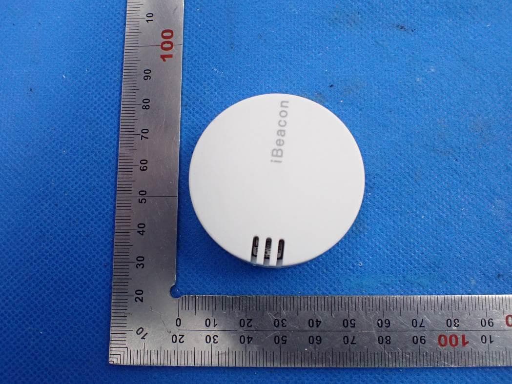
2AV9TDS-BEACON-06
Mar 23, 2021DS-Beacon-06
Equipment Class
DTS - Digital Transmission System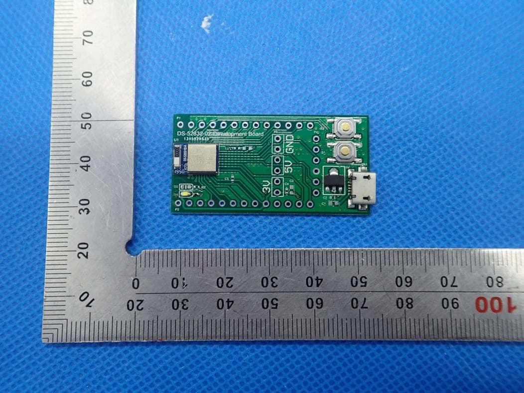
Jun 28, 2020
Equipment Class
DTS - Digital Transmission System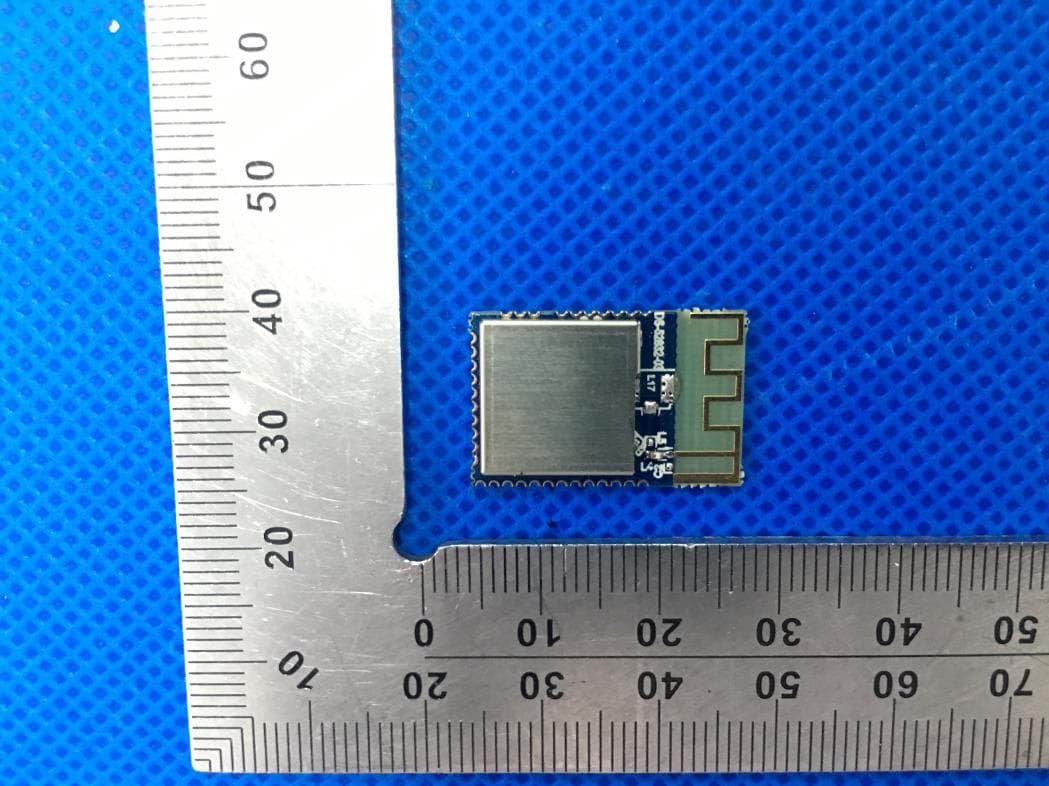
Jun 28, 2020
Equipment Class
DTS - Digital Transmission System