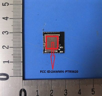
2AWMN-PTR5620PTR5620
Shenzhen Chuanghongxin Intelligent technology Co.,Ltd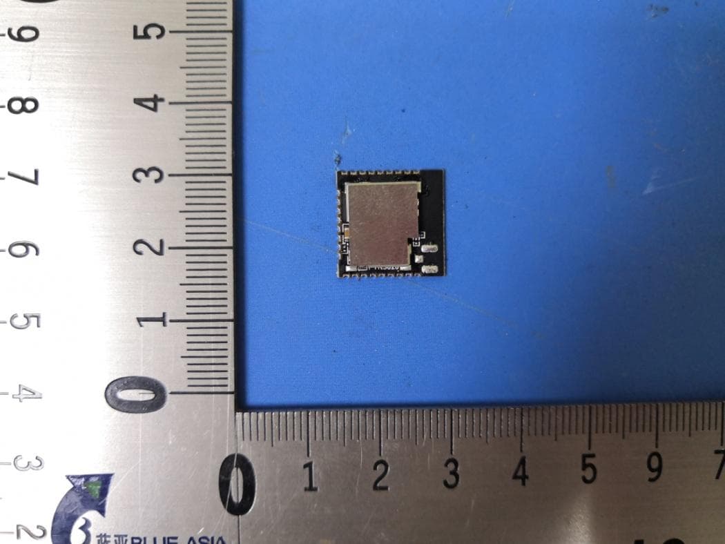
Click to zoom
Application Details
- Equipment Class
- DTS - Digital Transmission System
- Date of Grant
- Jul 19, 2020
- Application Purpose
- Original Equipment
- Date of Application
- Jul 12, 2020
- Equipment Note
- PTR5620
- Frequency Range
- 2402.00000000 - 2480.00000000
- Country
- China
Documents & Files
Document Text
Text extracted from the exhibit documents filed with the FCC. Open a document above to read the original.
Users Manual
ABLUE TECHNOLOGY COPYRIGHT ©2020 ALL RIGHTS RESERVED ABLUE TechnologyE-mail: [email protected] 1 Bluetooth 5.2 ready multi-protocol Module Embedded Cortex™ M4 32 bit processor Support Bluetooth Direct Finding AOA/AOD, MESH and Smart product The PTR5620 ultra-low power Bluetooth 5 ready multiprotocol System on Module based on the nRF52820 from Nordic Semiconductor. The module can support Bluetooth 5.2 by upgrading the protocol stack. The module with an ARM® Cortex™ M4 32 bit processor, 256KB Flash/32KB RAM, Bluetooth 5.1 Direct Finding AOA/AOD support , embedded 2.4GHz transceiver, provide a complete solution with no additional RF design, Bluetooth 5, allowing faster time to market, while simplifying designs, reducing BOM costs, also reduce the burden of Regulatory approvals to enter the world market. Making you more quickly into the Bluetooth smart application and remove the worries. Features PTR5620 Nordic nRF52820 with ARM Cortex M4 Multiprotocol support :Bluetooth 5.1, Bluetooth 5.1 Direction Finding AOA/AOD Bluetooth 5: 2 /1Mbps, 500 kbps, 125 kbps Integrated DC-DC converter Serial Wire Debug (SWD) Nordic SoftDevice Ready Over-the-Air (OTA) firmware update Flash/RAM: 256KB/32KB. 18 General purpose I/O pins low-power comparator with wake-up from System OFF mode 12 bit/200KSPSADC Two 2-wire Master/Slave (I2C compatible) 2 SPI Master/ 1 SPI Slave) 1 UART (with CTS/RTS and DMA) USB 2.0 full speed (12 Mbps) controller 20 channel CPU independent Programmable Peripheral Interconnect (PPI). Quadrature Demodulator (QDEC) 128-bit AES HW encryption 4 x 32 bits timers, 2 xReal Time Counters (RTC) PCB antenna Sizes: 15.4x15.4 x1.8mm DC/DC on board No external components required Operation voltage: 1.7V to 5.5V ABLUE TECHNOLOGY COPYRIGHT ©2020 ALL RIGHTS RESERVED ABLUE TechnologyE-mail: [email protected] 2 Typical Applications: 2.4 GHz Bluetooth low energy systems Proprietary 2.4 GHz systems Sports and leisure equipment Mobile phone accessories, ConnectedAppliances Health Care and Medical Consumer Electronics, Game pads Human Interface Devices, Remote control Building environment control / monitoring RFID, SecurityApplications,Low-Power Sensors Bluetooth Low Energy GateWay iBeacons™, Eddystone™, Indoor navigation Lighting Products Fitness devices, Wearables Quick Specifications: Multi-protocol VersionBluetooth 5.2 SecurityAES-128 Radio Frequency2.402GHz to 2.480GHz ModulationsGFSK at 2/1 Mbps, Long range 125/500kbps, 802.15.4- 250 kbps Receiver sensitivity-103dBm@BLE 125kbps(long range), -95dBm@BLE 1M AntennaIntegrated PCBAntenna / Ext. IPXAntenna Current Consumption TX only @ +8 dBm @ 3V, DC/DC enabled14.0 mA TX only @ 0 dBm @ 3V, DC/DC enabled4.9 mA RX only @ 1 Mbps @ 3V, DC/DC enabled4.7 mA CPU @ 64MHz from flash @ 3V, DC/DC3.3 mA System On1.5 μA System Off0.6μA Operating conditions Power supply1.7~5.5V Operating temperature-25~+85 °C ABLUE TECHNOLOGY COPYRIGHT ©2020 ALL RIGHTS RESERVED ABLUE TechnologyE-mail: [email protected] 3 Block diagram: Pin Description of Module(Top View): ABLUE TECHNOLOGY COPYRIGHT ©2020 ALL RIGHTS RESERVED ABLUE TechnologyE-mail: [email protected] 4 PinNameDescriptionRecommend usage Pin1P0.17Digital I/OStandard drive, low frequency I/O Pin2P0.18/RESETDigital I/O/ RESET Pin3P0.16Digital I/OStandard drive, low frequency I/O Pin4P0.20Digital I/O Pin5SWDCLKHW debug and programming Pin6SWDIOHW debug and programming Pin7P0.15Digital I/O Pin8P0.14Digital I/O Pin9P0.07Digital I/O Pin10D+USB D+USB Pin11D-USB D-USB Pin12VBUSUSB Power5 V input for USB 3.3 V regulator Pin13VDDHHigh voltage power supply Pin14P0.06Digital I/O Pin15P0.05/AIN3Digital I/O/Analog input 3 Pin16P0.01/XL2Reserve for 32.768KHz use Pin17P0.00/XL1Reserve for 32.768KHz use Pin18P0.04/AIN2Digital I/O/Analog input 2 Pin19P0.02/AIN0Digital I/O/Analog input 0 Pin20P0.03/AIN1Digital I/O/Analog input 1Standard drive, low frequency I/O Pin21P0.28Digital I/OStandard drive, low frequency I/O Pin22P0.30Digital I/OStandard drive, low frequency I/O Pin23VDDPower Supply Pin24GNDGround Pin25P0.29Digital I/OStandard drive, low frequency I/O Pin26P0.08Digital I/OStandard drive, low frequency I/O *Low frequency I/O is signals with a frequency up to 10 kHz *Internal 32.768 kHz RC oscillator is used to provide low frequency clock by default. If you want to use an external crystal, you can use the reserved pins (Pin16 and Pin17) to connect the external crystal and modify the firmware configuration. Note: An internal 4.7μF bulk capacitor has been included on the module. For those application that with heavy GPIO usage and/or current draw, it is good design practice to add additional bulk capacitance as required for your application. General Purpose I/O: Each GPIO can be accessed individually with the following user configurable features: Input/output direction Output drive strength Internal pull-up and pull-down resistors Wake-up from high or low level triggers on all pins Trigger interrupt on all pins ABLUE TECHNOLOGY COPYRIGHT ©2020 ALL RIGHTS RESERVED ABLUE TechnologyE-mail: [email protected] 5 All pins can be used by the PPI task/event system; the maximum number of pins that can be interfaced through the PPI at the same time is limited by the number of GPIOTE channels All pins can be individually configured to carry serial interface or quadrature demodulator signals Hardware RESET: There is on-chip power-on reset circuitry, But can still be used in external reset mode, in this case, GPIO pin P0.18 as an external hardware reset pin. In order to utilize P0.18 as a hardware reset, the UICR registers PSELRESET[0] and PSELRESET[1] must be set alike, to the value of 0x7FFFFF12. When P0.18 is programmed as RESET, the internal pull-up is automatically enabled. HW debug and flash programming of Module : The Module support the two pin Serial Wire Debug (SWD) interface and offers flexible and powerful mechanism for non-intrusive debugging of program code. Breakpoints, sing…
Text truncated - open the document above for the full version.
Attestation Statements
Compliance list INTEGRATIO N INST RUCTIO NS for 996369 D03 O EM the and 996369 D03 O EM b y Section s 2.2 thro ugh 2.10. Requirement Yes N/A Comment 2.2 List of applicable FCC rules List the FCC rules that are applicable to the modular transmitter. These are the rules that specifically establish the bands of operation, the power, spurious emissions, and operating fundamental frequencies. DO NOT list compliance to unintentional-radiator rules (Part 15 Subpart B) since that is not a condition of a module grant that is extended to a host manufacturer. See also Section 2.10 below concerning the need to notify host manufacturers that further testing is required.3 YES Refer to instruction FCC standards: FCC CFR Ti tle 47 Part 15 Subpart C Section 15.247 2.3 Summarize the specific operational use conditions Describe use conditions that are applicable to the modular transmitter, including for example any limits on antennas, etc. For example, if point-to-point antennas are used that require reduction in power or compensation for cable loss, then this information must be in the instructions. If the use condition limitations extend to professional users, then instructions must state that this information also extends to the host manufacturer’s instruction manual. In addition, certain information may also be needed, such as peak gain per frequency band and minimum gain, specifically for master devices in 5 GHz DFS bands. YES Refer to instruction Integral antenna with antenna gain 0 dBi 2.4 Limited module procedures If a modular transmitter is approved as a “limited module,” then the module manufacturer is responsible for approving the host envir onment that the limited module is used with. The manufacturer of a limited module must describe, both in the f iling and in the installat ion instruct ions , the alternative means that the limited module manufacturer uses to verify that the host meets the necessary requirements to satisfy the module limit ing cond it ions . A limited module manufacturer has the flexibility to define its alternat ive method to address the condit ions that limit t he init ia l approval, such as: shie lding, minimum N/A Not applicable signa ling amplitude, buffered modulat ion/data inputs , or power supply regulat ion. The alternative method could inc lude that the limited module manufacturer reviews detailed test data or host designs prior to giving the host manufacturer approval. This limited module procedure is also applicable for RF exposure evaluation when it is necessary to demonstrate compliance in a specific host. The module manufacturer must state how control of the product int o which the modular transmitter will be insta lled will be mainta ined such that full compliance of the product is always ensured. For addit iona l hosts other than the specific host or iginally granted with a limited module, a Class II permissive change is required on the module grant to register the addit iona l host as a specific host also approved wit h the module. 2.5 Trace antenna designs For a modular transmitter with trace antenna designs, see the guidance in Question 11 of KDB Publ i cati on 996369 D02 FAQ – Modules for Micro-Strip Antennas and traces. The integration information shall include for the TCB review the integration instructions for the following aspects: layout of trace design, parts list (BOM), antenna, connectors, and isolation requi rements. 4 a) Information that includes permitted variances (e.g., trace boundary limits , thickness, lengt h, w idth, shape(s) , die le c tr ic constant, and impedance as applicable for each type of antenna); b) Each design sha ll be considered a different type (e.g., antenna length in mult iple(s) of frequency, the wavelength, and antenna shape (traces in phase) can affect antenna gain and must be considered); c) The parameters shall be provided in a manner permitting host manufacturers to design the pr inted circuit (P C) board layout; d) Appropr iate parts by manufacturer and specifications; e) Test procedures for design ve r if ic a tion; and N/A Not applicable f) Production test procedures for ensuring compliance. The module grantee shall provide a noti ce that any de vi ati on( s ) f rom the de fi ne d parameters of the antenna trace, as described by the instructions, require that the host product manufacturer must notify the module grantee that they wish to change the antenna trace design. In this case, a Class II permissive change application is required to be filed by the grantee, or the host manufacturer can take responsibility through the change in FCC ID (new application) procedure followed by a Class II permissive change application. 2.6 RF exposure considerations It is essential for module grantees to clearly and explicitly state the RF exposure conditions that permit a host product manufacturer to use the module. Two types of instructions are required for RF exposure information: (1) to the host product manufacturer, to define the application conditions (mobile, portable – xx cm from a person’s body); and (2) additional text needed for the host product manufacturer to provide to end users in their end-product manuals. If RF exposure statements and use conditions are not provided, then the host product manufacturer is required to take responsibility of the module through a change in FCC I D ( ne w application). YES Refer to instruction This modular complies with FCC RF radiation exposure limits set forth for an uncontrolled environment. This transmitter must not be co-located or operating in conjunction with any other antenna or transmitter. 2.7 Antennas A list of antennas inc luded in the application for certification must be provided in the instruct ions. For modular transmitters approved as limited modules, all applicable professiona l installer instructions must be inc luded as part of the informat ion to the host product manufacturer. The antenna list shall also ident ify the antenna types (monopole, P IFA, dipole, etc. (n…
Text truncated - open the document above for the full version.
External Photos
Model No.: PTR5620
Internal Photos
Model No.: PTR5620
RF Exposure Info
Page 1 of3 BlueAsia of Technical Services(Shenzhen) Co., Ltd. IOT Test Centre of BlueAsia,No. 448 Bulong Road, Bantian Street, Longgang District, Shenzhen, China Telephone: TEL: +86-755-28682673 FAX: +86-755-28682673 Email:[email protected] TEST REPORT Product Name : Bluetooth module Brand Mark : ABLUE TECH Model No. : PTR5620 FCC ID : 2AWMN-PTR5620 Report Number : BLA-EMC-202006-A3702 Date of Sample Receipt : 2020/6/15 Date of Test : 2020/7/6 to 2020/7/6 Date of Issue : 2020/7/6 Test Standard : 47 CFR Part 1.1307, Part 2.1093, KDB 447498 Test Result : Pass Prepared for: SHENZHEN CHUANGHONGXIN INTELLIGENT TECHNOLOGY CO.,LTD Room703 of Block WanHai Building B, 1031 South Sea Avenue, Nanshan district, Shenzhen, China Prepared by: BlueAsia of Technical Services(Shenzhen) Co.,Ltd. IOT Test Centre of BlueAsia No. 448 Bulong Road, Bantian Street, Longgang District, Shenzhen,China TEL: +86-755-28682673 FAX: +86-755-28682673 Compiled by: Review by: Approved by: Date: 2020/7/6 Report No.: BLA-EMC-202006-A3702 Page 2 of3 BlueAsia of Technical Services(Shenzhen) Co., Ltd. IOT Test Centre of BlueAsia,No. 448 Bulong Road, Bantian Street, Longgang District, Shenzhen, China Telephone: TEL: +86-755-28682673 FAX: +86-755-28682673 Email:[email protected] RF EXPOSURE EVALUATION 1.1 RF Exposure Compliance Requirement 1.1.1 Standard Requirement According to KDB447498D01 General RF Exposure Guidance v06 Standalone SAR test exclusion considerations Unless specifically required by the published RF exposure KDB procedures, standalone 1-g head or body and 10-g extremity SAR evaluation for general population exposure conditions, by measurement or numerical simulation, is not required when the corresponding SAR Exclusion Threshold condition, listed below, is satisfied. 1.1.2 Limits The 1-g and 10-g SAR test exclusion thresholds for 100 MHz to 6 GHz at test separation distances ≤ 50 mm are determined by: [(max. power of channel, including tune-up tolerance, mW)/(min. test separation distance, mm)] · [√f(GHz)] ≤ 3.0 for 1-g SAR and ≤ 7.5 for 10-g extremity SAR, where f(GHz) is the RF channel transmit frequency in GHz Power and distance are rounded to the nearest mW and mm before calculation 17 The result is rounded to one decimal place for comparison The test exclusions are applicable only when the minimum test separation distance is ≤ 50 mm and for transmission frequencies between 100 MHz and 6 GHz. When the minimum test separation distance is < 5 mm, a distance of 5 mm is applied to determine SAR test exclusion Report No.: BLA-EMC-202006-A3702 Page 3 of3 BlueAsia of Technical Services(Shenzhen) Co., Ltd. IOT Test Centre of BlueAsia,No. 448 Bulong Road, Bantian Street, Longgang District, Shenzhen, China Telephone: TEL: +86-755-28682673 FAX: +86-755-28682673 Email:[email protected] 1.1.3EUT RF EXPOSURE Operational Mode: BLE Channel Maximum Peak Conducted Output Power (dBm) Tune up tolerance (dB) Maximum tune-up Power (dBm) Maximum tune-up Power (mW) Calculated value Exclusion threshold 2402MHz -0.44 ±1 0.56 1.14 0.35 3 2442MHz -0.80 ±1 0.2 1.05 0.33 3 2480MHz -1.11 ±1 -0.11 0.97 0.31 3 Conclusion: the calculated value ≤3.0, SAR is exempted. ----END OF REPORT---- The test report is effective only with both signature and specialized stamp, The result(s) shown in this report refer only to the sample(s) tested. Without written approval of BlueAsia, this report can’t be reproduced except in full.
Test Report
Page 1 of56 BlueAsia of Technical Services(Shenzhen) Co., Ltd. IOT Test Centre of BlueAsia,No. 448 Bulong Road, Bantian Street, Longgang District, Shenzhen, China Telephone: TEL: +86-755-28682673 FAX: +86-755-28682673 Email:[email protected] TEST REPORT Product Name : Bluetooth module Brand Mark : ABLUE TECH Model No. : PTR5620 FCC ID : 2AWMN-PTR5620 Report Number : BLA-EMC-202006-A3701 Date of Sample Receipt : 2020/6/15 Date of Test : 2020/6/15 to 2020/7/6 Date of Issue : 2020/7/6 Test Standard : 47 CFR Part 15, Subpart C 15.247 Test Result : Pass Prepared for: SHENZHEN CHUANGHONGXIN INTELLIGENT TECHNOLOGY CO.,LTD Room703 of Block WanHai Building B, 1031 South Sea Avenue, Nanshan district, Shenzhen, China Prepared by: BlueAsia of Technical Services(Shenzhen) Co.,Ltd. IOT Test Centre of BlueAsia No. 448 Bulong Road, Bantian Street, Longgang District, Shenzhen,China TEL: +86-755-28682673 FAX: +86-755-28682673 Compiled by: Review by: Approved by: Date: 2020/7/6 Report No.: BLA-EMC-202006-A3701 Page 2 of56 BlueAsia of Technical Services(Shenzhen) Co., Ltd. IOT Test Centre of BlueAsia,No. 448 Bulong Road, Bantian Street, Longgang District, Shenzhen, China Telephone: TEL: +86-755-28682673 FAX: +86-755-28682673 Email:[email protected] REPORT REVISE RECORD Version No. Date Description 00 2020/7/6 Original Report No.: BLA-EMC-202006-A3701 Page 3 of56 BlueAsia of Technical Services(Shenzhen) Co., Ltd. IOT Test Centre of BlueAsia,No. 448 Bulong Road, Bantian Street, Longgang District, Shenzhen, China Telephone: TEL: +86-755-28682673 FAX: +86-755-28682673 Email:[email protected] TABLE OF CONTENTS 1 TEST SUMMARY ........................................................................................................................................6 2 GENERAL INFORMATION .........................................................................................................................7 3 GENERAL DESCRIPTION OF E.U.T. .........................................................................................................7 4 TEST ENVIRONMENT ................................................................................................................................8 5 TEST MODE ................................................................................................................................................8 6 MEASUREMENT UNCERTAINTY ..............................................................................................................8 7 DESCRIPTION OF SUPPORT UNIT...........................................................................................................9 8 LABORATORY LOCATION .........................................................................................................................9 9 TEST INSTRUMENTS LIST ..................................................................................................................... 10 1 CONDUCTED EMISSIONS AT AC POWER LINE (150KHZ-30MHZ)..................................................... 14 1.1 LIMITS ................................................................................................................................................................... 14 1.2 BLOCK DIAGRAM OF TEST SETUP .......................................................................................................................... 14 1.3 PROCEDURE .......................................................................................................................................................... 14 1.4 TEST DATA .............................................................................................................................................................. 16 2 CONDUCTED BAND EDGES MEASUREMENT ..................................................................................... 18 2.1 LIMITS ................................................................................................................................................................... 18 2.2 BLOCK DIAGRAM OF TEST SETUP .......................................................................................................................... 18 2.3 TEST DATA .............................................................................................................................................................. 19 3 RADIATED SPURIOUS EMISSIONS ....................................................................................................... 20 3.1 LIMITS ................................................................................................................................................................... 20 3.2 BLOCK DIAGRAM OF TEST SETUP .......................................................................................................................... 21 3.3 PROCEDURE .......................................................................................................................................................... 21 3.4 TEST DATA .............................................................................................................................................................. 23 4 RADIATED EMISSIONS WHICH FALL IN THE RESTRICTED BANDS................................................. 28 4.1 LIMITS ................................................................................................................................................................... 28 4.2 BLOCK DIAGRAM OF TEST SETUP .......................................................................................................................... 29 4.3 PROCEDURE .......................................................................................................................................................... 29 4.4 TEST DATA .............................................................................................................................................................. 31 5 CONDUCTED SPUR…
Text truncated - open the document above for the full version.
Test Setup Photos
Model No.: PTR5620
Contact Information
Applicant
Tan Hui(Manager)
Test Firm
BlueAsia of Technical Services (Shenzhen)Blue Zheng
[email protected]+86 755-23059481-815
Technical Specifications
| # | Rule Parts | Frequency Range | Power Output |
|---|---|---|---|
| 1 | 15C | 2.40 GHz - 2.48 GHz | 904.00 µW |
Other Applications from Shenzhen Chuanghongxin Intelligent technology Co.,Ltd
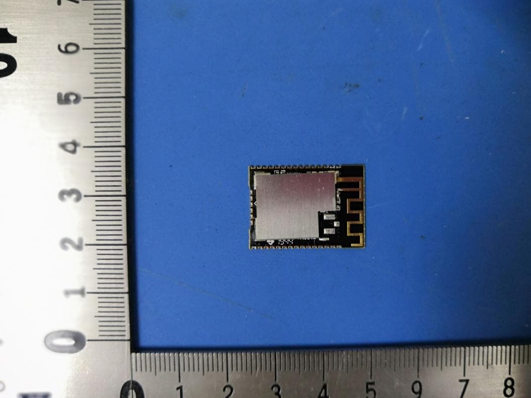
2AWMN-PTR9813
Jul 13, 2020Bluetooth module
Equipment Class
DTS - Digital Transmission System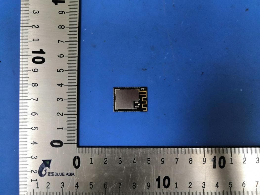
2AWMN-PTR9611
Jul 11, 2020PTR9611
Equipment Class
DTS - Digital Transmission System