2AXAA-HN030-01Li Qiu Yong
CWCE Lighting (Shenzhen) Co., Ltd.
Click to zoom
Application Details
- Equipment Class
- DTS - Digital Transmission System
- Date of Grant
- Nov 06, 2020
- Application Purpose
- Original Equipment
- Date of Application
- Nov 06, 2020
- Equipment Note
- Li Qiu Yong
- Frequency Range
- 2402.00000000 - 2480.00000000
- Country
- China
Documents & Files
Document Text
Text extracted from the exhibit documents filed with the FCC. Open a document above to read the original.
Users Manual
User Manual WIFI MODULE Model No: HN030-01 FCC ID: 2AXAA-HN030-01
Attestation Statements
Compliance list INTEGRATION INSTRUCTIONS for 996369 D03 OEM the and 996369 D03 OEM by Sections 2.2 through 2.10. Requirement Yes N/A Comment 2.2 List of applicable FCC rules List the FCC rules that are applicable to the modular transmitter. These are the rules that specifically establish the bands of operation, the power, spurious emissions, and operating fundamental frequencies. DO NOT list compliance to unintentional-radiator rules (Part 15 Subpart B) since that is not a condition of a module grant that is extended to a host manufacturer. See also Section 2.10 below concerning the need to notify host manufacturers that further testing is required.3 YES Refer to instruction FCC standards: FCC CFR Title 47 Part 15 Subpart C Section 15.247 2.3 Summarize the specific operational use conditions Describe use conditions that are applicable to the modular transmitter, including for example any limits on antennas, etc. For example, if point-to-point antennas are used that require reduction in power or compensation for cable loss, then this information must be in the instructions. If the use condition limitations extend to professional users, then instructions must state that this information also extends to the host manufacturer’s instruction manual. In addition, certain information may also be needed, such as peak gain per frequency band and minimum gain, specifically for master devices in 5 GHz DFS bands. YES Refer to instruction Integral PCB antenna with antenna gain 0dBi 2.4 Limited module procedures If a modular transmitter is approved as a “limited module,” then the module manufacturer is responsible for approving the host environment that the limited module is used with. The manufacturer of a limited module must describe, both in the filing and in the installation instructions, the alternative means that the limited module manufacturer uses to verify that the host meets the necessary requirements to satisfy the module limiting conditions. A limited module manufacturer has the flexibility to define its alternative method to address the conditions that limit the initial approval, such as: shielding, minimum N/A Not applicable signaling amplitude, buffered modulation/data inputs, or power supply regulation. The alternative method could include that the limited module manufacturer reviews detailed test data or host designs prior to giving the host manufacturer approval. This limited module procedure is also applicable for RF exposure evaluation when it is necessary to demonstrate compliance in a specific host. The module manufacturer must state how control of the product into which the modular transmitter will be installed will be maintained such that full compliance of the product is always ensured. For additional hosts other than the specific host originally granted with a limited module, a Class II permissive change is required on the module grant to register the additional host as a specific host also approved with the module. 2.5 Trace antenna designs For a modular transmitter with trace antenna designs, see the guidance in Question 11 of KDB Publication 996369 D02 FAQ – Modules for Micro-Strip Antennas and traces. The integration information shall include for the TCB review the integration instructions for the following aspects: layout of trace design, parts list (BOM), antenna, connectors, and isolation requirements. 4 a) Information that includes permitted variances (e.g., trace boundary limits, thickness, length, width, shape(s), dielectric constant, and impedance as applicable for each type of antenna); b) Each design shall be considered a different type (e.g., antenna length in multiple(s) of frequency, the wavelength, and antenna shape (traces in phase) can affect antenna gain and must be considered); c) The parameters shall be provided in a manner permitting host manufacturers to design the printed circuit (PC) board layout; d) Appropriate parts by manufacturer and specifications; e) Test procedures for design verification; and N/A Not applicable f) Production test procedures for ensuring compliance. The module grantee shall provide a notice that any deviation(s) from the defined parameters of the antenna trace, as described by the instructions, require that the host product manufacturer must notify the module grantee that they wish to change the antenna trace design. In this case, a Class II permissive change application is required to be filed by the grantee, or the host manufacturer can take responsibility through the change in FCC ID (new application) procedure followed by a Class II permissive change application. 2.6 RF exposure considerations It is essential for module grantees to clearly and explicitly state the RF exposure conditions that permit a host product manufacturer to use the module. Two types of instructions are required for RF exposure information: (1) to the host product manufacturer, to define the application conditions (mobile, portable – xx cm from a person’s body); and (2) additional text needed for the host product manufacturer to provide to end users in their end-product manuals. If RF exposure statements and use conditions are not provided, then the host product manufacturer is required to take responsibility of the module through a change in FCC ID (new application). YES Refer to instruction The modular can be installed or integrated in mobile or fix devices only. This modular cannot be installed in any portable device If not to apply for any further FCC approval related to SAR,etc. This modular complies with FCC RF radiation exposure limits set forth for an uncontrolled environment. This transmitter must not be co-located or operating in conjunction with any other antenna or transmitter. This modular must be installed and operated with a minimum distance of 20 cm between the radiator and user body. 2.7 Antennas A list of antennas included in the application for certification must be provided in the instructions. For modular transmitters approved as li…
Text truncated - open the document above for the full version.
Attestation Statements
Single Modular approval declaration letter We, CWCE Lighting (Shenzhen) Co., Ltd. apply Single modular approval for Product Name: WIFI MODULE Model: HN030-01 FCC ID: 2AXAA-HN030-01 According to 996369 D01 Module Equip Auth Guide v01r04 and 15.212 requirement: 1) The radio elements must have the radio frequency circuitry shielded. Physical components and tuning capacitor(s) may be located external to the shield, but must beon the module assembly; Answer :Yes, both side shielded 2)The module must have buffered modulation/data inputs to ensure that the device will comply with Part 15 requirements with any type of input signal; Answer :Yes, All inputs to the modules are buffered through logic or microprocessor inputs. 3)The modular transmitter must have its own power supply regulation. Answer :Yes, A low drop out regulator is used for modular power supply regulation. 4)The module must contain a permanently attached antenna, or contain a unique antenna connector, and be marketed and operated only with specific antenna(s), per Sections 15.203, 15.204(b), 15.204(c), 15.212(a), 2.929(b); Answer :Yes, Device is equipped with PCB antenna. (5)The module must demonstrate compliance in a stand-alone configuration; Answer :Yes, distance between modular and all AEs are longer than 10cm ,refer to setup photo. (6) The module must be labelled with its permanently affixed FCC ID label, or use an electronic display (See KDB Publication 784748 about labelling requirements); Answer :Yes, The modular has a permanent fixed label, and below statement was listed in the User Manual; The host device must be labeled to display the FCC ID of the module Contains FCC ID: 2AXAA-HN030-01 (7)The module must comply with all specific rules applicable to the transmitter including all the conditions provided in the integration instructions by the grantee; Answer :Yes, The module comply with all specific rules applicable to the transmitter including all the conditions provided in the integration instructions by the grantee, Refer to test report and user manual . (8)The module must comply with RF exposure requirements Answer :Yes, Transmitter meets MPE calculation of 47 CFR 1.1307 . Refer to MPE Reports and Refer to modular installation manual <Signature> Name: Li Qiu Yong Title: Manager Applicant Company: CWCE Lighting (Shenzhen) Co., Ltd.
Cover Letter(s)
DATE :2020.09.29 Equipment Autorisation Division Federal Communications Commission 7435 Oakland Mills Road Columbia, MD 21046 FCC ID: _ 2AXAA-HN030-01 __ Product Name: _ WIFI MODULE _____ Request for Confidentiality Pursuant to Sections 0.457 and 0.459 of the commission’s rules, we hereby request that the following documents be held confidential: (List here the documents for which you are seeking confidentiality – for example ...) Schematics Block diagram Operation description These materials contain trade secrets and proprietary information and are not customarily released to the public. The public disclosure of this information might be harmful to the company and provide unjustified benefits to our competitors. <Signature> Name: Li Qiu Yong Title: Manager Applicant Company: CWCE Lighting (Shenzhen) Co., Ltd.
External Photos
Dongguan New Testing Centre Co., Ltd E-mail: [email protected] 3F, No. 1 the 1st North Industry Road, Songshan Lake Science & Technology Park, Dongguan, Guangdong, China, 523808 Page 42 of 44 Report No.: NTC-ER2009024 12. Photos of the EUT
Internal Photos
Dongguan New Testing Centre Co., Ltd E-mail: [email protected] 3F, No. 1 the 1st North Industry Road, Songshan Lake Science & Technology Park, Dongguan, Guangdong, China, 523808 Page 43 of 44 Report No.: NTC-ER2009024 Dongguan New Testing Centre Co., Ltd E-mail: [email protected] 3F, No. 1 the 1st North Industry Road, Songshan Lake Science & Technology Park, Dongguan, Guangdong, China, 523808 Page 44 of 44 Report No.: NTC-ER2009024 --END OF REPORT--
RF Exposure Info
SAR evaluation MPE Calculation Method E (V/m) = (30*P*G) 0.5 /d Power Density: Pd (W/m2) = E 2 /377 E = Electric Field (V/m) P = Peak RF output Power (W) G = EUT Antenna numeric gain (numeric) d = Separation distance between radiator and human body (m) The formula can be changed to Pd = (30*P*G) / (377*d 2 ) From the peak EUT RF output power, the minimum mobile separation distance, d=0.2m, as well as the gain of the used antenna, the RF power density can be obtained. Calculated Result and Limit (WORSE CASE IS AS BELOW) Directional AntennaGain (Numeric) Peak Output Power (mW) Power Density (S)(mW/cm2) Limit of Power Density (S) (mW/cm2) Test Result 1(0 dBi) 26.841 (14.288dBm@2412MHz) 0.00534 1 Compiles
Test Report
FCC TEST REPORT Tested Laboratory DONGGUAN NEW TESTING CENTRE CO., LTD ◎Address: 3F, No. 1 the 1st North Industry Road, Songshan Lake Science & Technology Park, Dongguan, Guangdong, China, 523808 A2LA Number:5426.01 ISED#: 25295, CAB identifier: CN0087 Tel: +86-769-22212079 Web: http://www.ntc-cert.com E-mail: [email protected] Report No. ...................................... : NTC-ER2009023 Applicant’s name ........................... : Shenzhen CWCE Lighting Technology Co.,Ltd. Address .......................................... : A/area, 9F/Bldg,Cuijing Rd 28, Longtian Town,Pingshan New District,SHENZHEN Guangdong China 518122 Dongguan New Testing Centre Co., Ltd E-mail: [email protected] 3F, No. 1 the 1st North Industry Road, Songshan Lake Science & Technology Park, Dongguan, Guangdong, China, 523808 Page 1 of 85 Report No.:NTC-ER2009023 TABLE OF CONTENTS TEST REPORT DECLARE ............................................................................................................ 3 1. Summary of test results ........................................................................................................... 4 2. General test information .......................................................................................................... 5 2.1. Detail models ............................................................................................................................. 7 2.2. Test Peripheral List ................................................................................................................... 7 2.3. Block diagram EUT configuration for test ............................................................................. 8 2.4. Test environment conditions ................................................................................................... 8 2.5. Measurement uncertainty ........................................................................................................ 8 3. Power Line Conducted Emission Test .................................................................................. 9 3.1. Test equipment ......................................................................................................................... 9 3.2. Block diagram of test setup ..................................................................................................... 9 3.3. Power Line Conducted Emission Limits (Class B) .............................................................. 9 3.4. Test Procedure ........................................................................................................................ 10 3.5. Test Result ............................................................................................................................... 10 4. Radiated emission test ........................................................................................................... 13 4.1. Test equipment ....................................................................................................................... 13 4.2. Block diagram of test setup ................................................................................................... 14 4.3. Limit .......................................................................................................................................... 16 4.4. Test Procedure ........................................................................................................................ 17 4.5. Test result ................................................................................................................................ 17 5. Output Power .......................................................................................................................... 32 5.1. Test equipment ....................................................................................................................... 32 5.2. Block diagram of test setup ................................................................................................... 32 5.3. Limit .......................................................................................................................................... 32 5.4. Test Procedure ........................................................................................................................ 32 5.5. Test result ................................................................................................................................ 33 6. -6dB Bandwidth ....................................................................................................................... 40 6.1. Test equipment ....................................................................................................................... 40 6.2. Block diagram of test setup ................................................................................................... 40 6.3. Limit .......................................................................................................................................... 40 6.4. Test Procedure ........................................................................................................................ 40 6.5. Test result ................................................................................................................................ 41 7. Band Edges Measurement .................................................................................................... 48 7.1. Test equipment ....................................................................................................................... 48 Dongguan New Testing Centre Co., Ltd E-mail: [email protected] 3F, No. 1 the 1st North Industry Road, Songshan Lake Science & Technology Park, Dongguan, Guangdong, China, 523808 Page 2 of 85 Report No.:NTC-ER2009023 7.2. Block diagram of test setup ................................................................................................... 48 7…
Text truncated - open the document above for the full version.
Test Report
Dongguan New Testing Centre Co., Ltd E-mail: [email protected] 3F, No. 1 the 1st North Industry Road, Songshan Lake Science & Technology Park, Dongguan, Guangdong, China, 523808 Page 43 of 85 Report No.: NTC-ER2009023 Condition Mode Frequency (MHz) Antenna 99% OBW (MHz) -6 dB Bandwidth (MHz) Limit -6 dB Bandwidth (MHz) Verdict NVNT 802.11g 54Mbps 2412 Ant 1 16.2003 15.8014 0.5 Pass NVNT 802.11g 54Mbps 2437 Ant 1 16.3344 15.7641 0.5 Pass NVNT 802.11g 54Mbps 2462 Ant 1 16.2504 14.5372 0.5 Pass OBW NVNT 802.11g 54Mbps 2412MHz Ant1 Dongguan New Testing Centre Co., Ltd E-mail: [email protected] 3F, No. 1 the 1st North Industry Road, Songshan Lake Science & Technology Park, Dongguan, Guangdong, China, 523808 Page 44 of 85 Report No.: NTC-ER2009023 OBW NVNT 802.11g 54Mbps 2437MHz Ant1 OBW NVNT 802.11g 54Mbps 2462MHz Ant1 Dongguan New Testing Centre Co., Ltd E-mail: [email protected] 3F, No. 1 the 1st North Industry Road, Songshan Lake Science & Technology Park, Dongguan, Guangdong, China, 523808 Page 45 of 85 Report No.: NTC-ER2009023 Condition Mode Frequency (MHz) Antenna 99% OBW (MHz) -6 dB Bandwidth (MHz) Limit -6 dB Bandwidth (MHz) Verdict NVNT 802.11n(HT20) 2412 Ant 1 16.4017 15.0507 0.5 Pass NVNT 802.11n(HT20) 2437 Ant 1 16.7791 11.0706 0.5 Pass NVNT 802.11n(HT20) 2462 Ant 1 17.0698 15.5565 0.5 Pass OBW NVNT 802.11n(HT20) 2412MHz Ant1 OBW NVNT 802.11n(HT20) 2437MHz Ant1 Dongguan New Testing Centre Co., Ltd E-mail: [email protected] 3F, No. 1 the 1st North Industry Road, Songshan Lake Science & Technology Park, Dongguan, Guangdong, China, 523808 Page 46 of 85 Report No.: NTC-ER2009023 OBW NVNT 802.11n(HT20) 2462MHz Ant1 Condition Mode Frequency (MHz) Antenna 99% OBW (MHz) -6 dB Bandwidth (MHz) Limit -6 dB Bandwidth (MHz) Verdict NVNT 802.11n(HT40) 2422 Ant 1 35.6821 35.0468 0.5 Pass NVNT 802.11n(HT40) 2437 Ant 1 35.6912 34.9953 0.5 Pass NVNT 802.11n(HT40) 2452 Ant 1 35.8633 34.9155 0.5 Pass OBW NVNT 802.11n(HT40) 2422MHz Ant1 Dongguan New Testing Centre Co., Ltd E-mail: [email protected] 3F, No. 1 the 1st North Industry Road, Songshan Lake Science & Technology Park, Dongguan, Guangdong, China, 523808 Page 47 of 85 Report No.: NTC-ER2009023 OBW NVNT 802.11n(HT40) 2437MHz Ant1 OBW NVNT 802.11n(HT40) 2452MHz Ant1 Dongguan New Testing Centre Co., Ltd E-mail: [email protected] 3F, No. 1 the 1st North Industry Road, Songshan Lake Science & Technology Park, Dongguan, Guangdong, China, 523808 Page 48 of 85 Report No.: NTC-ER2009023 7. Band Edges Measurement 7.1. Test equipment Item Equipment Manufacturer Model No. Serial No. Last Cal. Cal. Interval 8. 1 MXA Signal Analyzer KEYSIGHT N9020A MY5451047 6 2020/05/25 1 Year 7.2. BLOCK DIAGRAM OF TEST SETUP 7.3. Limit Below –30dB of the highest emission level of operating band (In 100 kHz Resolution Bandwidth) 7.4. Test Procedure The transmitter output was connected to the spectrum analyzer via a low lose cable. Set RBW of spectrum analyzer to 100 KHz and VBW of spectrum analyzer to 300 KHz with convenient frequency span including 100 KHz bandwidth from band edge. Peak conducted output power measured within any 100 kHz outside the authorized frequency band shall be attenuated by at least 30dB relative to the maximum measured in-band peak PSD level. The band edges was measured and recorded. Dongguan New Testing Centre Co., Ltd E-mail: [email protected] 3F, No. 1 the 1st North Industry Road, Songshan Lake Science & Technology Park, Dongguan, Guangdong, China, 523808 Page 49 of 85 Report No.: NTC-ER2009023 7.5. Test result Condition Mode Frequency (MHz) Antenna Max Value (dBc) Limit (dBc) Verdict NVNT 802.11b 11Mbps 2412 Ant 1 -58.054 -30 Pass NVNT 802.11b 11Mbps 2462 Ant 1 -58.798 -30 Pass Band Edge NVNT 802.11b 11Mbps 2412MHz Ant1 Ref Dongguan New Testing Centre Co., Ltd E-mail: [email protected] 3F, No. 1 the 1st North Industry Road, Songshan Lake Science & Technology Park, Dongguan, Guangdong, China, 523808 Page 50 of 85 Report No.: NTC-ER2009023 Band Edge NVNT 802.11b 11Mbps 2412MHz Ant1 Emission Band Edge NVNT 802.11b 11Mbps 2462MHz Ant1 Ref Dongguan New Testing Centre Co., Ltd E-mail: [email protected] 3F, No. 1 the 1st North Industry Road, Songshan Lake Science & Technology Park, Dongguan, Guangdong, China, 523808 Page 51 of 85 Report No.: NTC-ER2009023 Band Edge NVNT 802.11b 11Mbps 2462MHz Ant1 Emission Condition Mode Frequency (MHz) Antenna Max Value (dBc) Limit (dBc) Verdict NVNT 802.11g 54Mbps 2412 Ant 1 -52.716 -30 Pass NVNT 802.11g 54Mbps 2462 Ant 1 -46.903 -30 Pass Band Edge NVNT 802.11g 54Mbps 2412MHz Ant1 Ref Dongguan New Testing Centre Co., Ltd E-mail: [email protected] 3F, No. 1 the 1st North Industry Road, Songshan Lake Science & Technology Park, Dongguan, Guangdong, China, 523808 Page 52 of 85 Report No.: NTC-ER2009023 Band Edge NVNT 802.11g 54Mbps 2412MHz Ant1 Emission Band Edge NVNT 802.11g 54Mbps 2462MHz Ant1 Ref Dongguan New Testing Centre Co., Ltd E-mail: [email protected] 3F, No. 1 the 1st North Industry Road, Songshan Lake Science & Technology Park, Dongguan, Guangdong, China, 523808 Page 53 of 85 Report No.: NTC-ER2009023 Band Edge NVNT 802.11g 54Mbps 2462MHz Ant1 Emission Condition Mode Frequency (MHz) Antenna Max Value (dBc) Limit (dBc) Verdict NVNT 802.11n(HT20) 2412 Ant 1 -51.991 -30 Pass NVNT 802.11n(HT20) 2462 Ant 1 -47.842 -30 Pass Band Edge NVNT 802.11n(HT20) 2412MHz Ant1 Ref Dongguan New Testing Centre Co., Ltd E-mail: [email protected] 3F, No. 1 the 1st North Industry Road, Songshan Lake Science & Technology Park, Dongguan, Guangdong, China, 523808 Page 54 of 85 Report No.: NTC-ER2009023 Band Edge NVNT 802.11n(HT20) 2412MHz Ant1 Emission Band Edge NVNT 802.11n(HT20) 2462MHz Ant1 Ref Dongguan New Testing Centre Co., Ltd E-mail: [email protected] 3F, No. 1 the 1st North Industry Road, Songshan Lake Science & Technology Park, Dongguan, Guangdong, China, 523808 Page 55 of 85 Report No.: NTC-ER2009023 Band Edge NVNT 802.11n(HT20) 2462MHz Ant1 Emission Condition Mode Frequency (MHz) Antenna Max Value (dBc) Limit (dBc) Verdict NVNT 802.11…
Text truncated - open the document above for the full version.
Test Report
FCC TEST REPORT Tested Laboratory: DONGGUAN NEW TESTING CENTRE CO., LTD ◎Address: 3F, No. 1 the 1st North Industry Road, Songshan Lake Science & Technology Park, Dongguan, Guangdong, China, 523808 A2LA Number:5426.01 ISED#: 25295, CAB identifier: CN0087 Tel: +86-769-22212079 Web: http://www.ntc-cert.com E-mail: [email protected] Report No. ...................................... : NTC-ER2009024 Applicant’s name ........................... : Shenzhen CWCE Lighting Technology Co.,Ltd. Address .......................................... : A/area, 9F/Bldg,Cuijing Rd 28, Longtian Town,Pingshan New District,SHENZHEN Guangdong China 518122 Dongguan New Testing Centre Co., Ltd E-mail: [email protected] 3F, No. 1 the 1st North Industry Road, Songshan Lake Science & Technology Park, Dongguan, Guangdong, China, 523808 Page 1 of 44 Report No.:NTC-ER2009024 TABLE OF CONTENTS TEST REPORT DECLARE ............................................................................................................ 3 1. Summary of test results ........................................................................................................... 4 2. General test information .......................................................................................................... 5 2.1. Detail models ............................................................................................................................. 7 2.2. Test Peripheral List ................................................................................................................... 7 2.3. Block diagram EUT configuration for test ............................................................................. 8 2.4. Test environment conditions ................................................................................................... 8 2.5. Measurement uncertainty ........................................................................................................ 8 3. Power Line Conducted Emission Test .................................................................................. 9 3.1. Test equipment ......................................................................................................................... 9 3.2. Block diagram of test setup ..................................................................................................... 9 3.3. Power Line Conducted Emission Limits (Class B) .............................................................. 9 3.4. Test Procedure ........................................................................................................................ 10 3.5. Test Result ............................................................................................................................... 10 4. Radiated emission test ........................................................................................................... 13 4.1. Test equipment ....................................................................................................................... 13 4.2. Block diagram of test setup ................................................................................................... 14 4.3. Limit .......................................................................................................................................... 16 4.4. Test Procedure ........................................................................................................................ 17 4.5. Test result ................................................................................................................................ 17 5. Output Power .......................................................................................................................... 23 5.1. Test equipment ....................................................................................................................... 23 5.2. Block diagram of test setup ................................................................................................... 23 5.3. Limit .......................................................................................................................................... 23 5.4. Test Procedure ........................................................................................................................ 23 5.5. Test result ................................................................................................................................ 24 6. -6dB Bandwidth ....................................................................................................................... 26 6.1. Test equipment ....................................................................................................................... 26 6.2. Block diagram of test setup ................................................................................................... 26 6.3. Limit .......................................................................................................................................... 26 6.4. Test Procedure ........................................................................................................................ 26 6.5. Test result ................................................................................................................................ 27 7. Band Edges Measurement .................................................................................................... 29 7.1. Test equipment ....................................................................................................................... 29 Dongguan New Testing Centre Co., Ltd E-mail: [email protected] 3F, No. 1 the 1st North Industry Road, Songshan Lake Science & Technology Park, Dongguan, Guangdong, China, 523808 Page 2 of 44 Report No.:NTC-ER2009024 7.2. Block diagram of test setup ................................................................................................... 29 …
Text truncated - open the document above for the full version.
Test Setup Photos
Setup photos Model No: HN030-01 Conducted emission test Radiated emission test 30MHz – 1GHz Above 1GHz
Contact Information
Applicant
Li Qiu Yong(Manager)
Test Firm
Dongguan New Testing Centre Co., LtdDave Gao
[email protected]86-15625558400
Technical Specifications
| # | Rule Parts | Frequency Range | Power Output |
|---|---|---|---|
| 3 | 15C | 2.40 GHz - 2.48 GHz | 887.00 µW |
Other Applications from CWCE Lighting (Shenzhen) Co., Ltd.
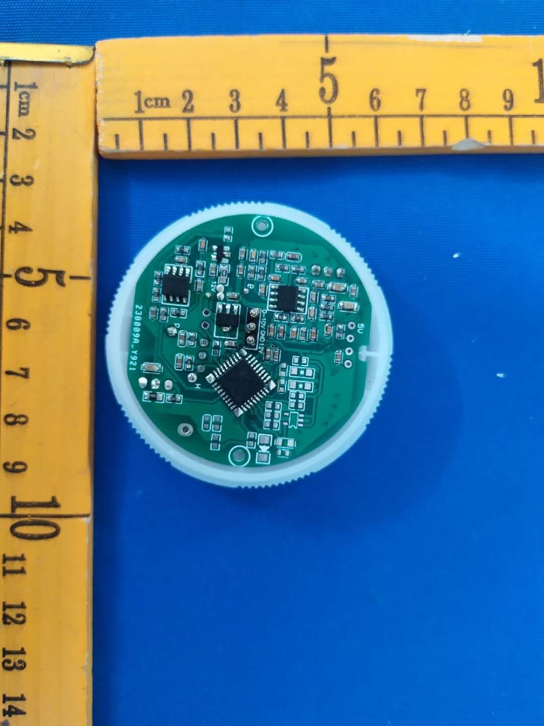
2AXAA-HN020-01V
Sep 14, 2020Microwave Motion Sensor
Equipment Class
DXX - Part 15 Low Power Communication Device Transmitter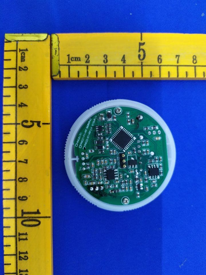
2AXAA-HN022-01V
Sep 14, 2020Microwave Motion Sensor
Equipment Class
DXX - Part 15 Low Power Communication Device Transmitter