2AXCP-CLEAR360Bluetooth headphone
Bongiovi Acoustic Labs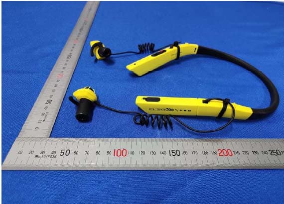
Click to zoom
Application Details
- Equipment Class
- DXX - Part 15 Low Power Communication Device Transmitter
- Date of Grant
- Nov 20, 2022
- Application Purpose
- Original Equipment
- Date of Application
- Nov 20, 2022
- Equipment Note
- Bluetooth headphone
- Frequency Range
- 2402.00000000 - 2480.00000000
- Company
- Bongiovi Acoustic Labs
- Country
- United States
Documents & Files
Document Text
Text extracted from the exhibit documents filed with the FCC. Open a document above to read the original.
Users Manual
& & USER MA ANUAL Page | 1 Page | 2 DISCLAIMER CLEAR 360 VENTURES makes no representations or warranties with respect to this manual and, to the maximum extent permitted by law, expressly limits its liability for breach of any warranty that may be implied to the replacement of this manual with another. Furthermore, CLEAR 360 VENTURESreserves the right to revise this publication at any time without incurring an obligation to notify any person of the revision. The information provided in this documentation contains general descriptions and/or technical characteristics of the operating procedures and performance of the products contained herein. This documentation is not intended as a substitute for and is not to be used for determining suitability or reliability of these products for specific user applications. It is the duty of any such users or product procurement/applications personnelto perform the appropriate and complete risk analysis, evaluation and testing of the products with respect to the relevant specific application or use thereof. Neither CLEAR 360 VENTURESnor any of its affiliates or subsidiaries shall be responsible or liable for misuse of the information that is contained herein. If you have any questions, suggestions for improvements or amendments, or believe you havefound errors in this publication, please notify us immediately using the contact information found at http://www.clear360products.com. All pertinent state, regional, and local safety regulations must be observed when using this product. For reasons of safety and to help ensure compliance with documented system data, only the manufacturer shall perform repairs to components. Failure to observe this information can result in personnel injury or equipment damage. Copyright © 2021 by CLEAR 360 VENTURES All rights reserved. No part of this publication may be reproduced, distributed, or transmitted in any form or by any means, including photocopying, recording, or other electronic or mechanical methods, without the prior written permission of the publisher. For permission requests, write to the publisher, addressed “Attention: Permissions Coordinator,” at the address below. CLEAR 360 VENTURES 649 SW Whitmore Drive Port Saint Lucie, FL 34984 TRADEMARKS CLEAR 360 VENTUREShas made every effort to supply trademark information about company names, products and services mentioned in this manual. Trademarks shown below were derived from various sources. All trademarks are the property of their respective owners. General Notice:Some product names used in this manual are used for identification purposes only and may be trademarks of their respective companies. Page | 3 Table of Contents 1 PREFACE .......................................................................................................................................... 1.1 ..... Conventions Used in This Manual ................................................................................................... 1.2 ..... Explanation of Safety Terminology Used [ref. ANSI Z535.4‐2011 (R2017)] ..................................... 1.3 ..... Retaining Instructions ..................................................................................................................... 1.4 ..... Obtaining Documentation and Information ................................................................................... 1.4.1 Internet .......................................................................................................................... 1.4.2 Ordering Documentation ............................................................................................... 1.4.3 Other languages ............................................................................................................. 1.4.4 Documentation Feedback .............................................................................................. 1.4.5 Support and service ....................................................................................................... 2 PRODUCT DESCRIPTION .................................................................................................................. 2.1 ..... Package Contents ........................................................................................................................... 2.2 ..... Intended Use ................................................................................................................................... 2.3 ..... System Overview ............................................................................................................................. 2.4 ..... Technical Data ................................................................................................................................ 2.5 ..... Product Compliance ........................................................................................................................ 2.5.1 Certificate of Compliance‐Restriction of the use of Hazardous Substances (RoHs) .................................................................................................................................... . 2.5.2 Certificate of Compliance‐Registration, Evaluation, Authorization and Restriction of Chemicals (REACh) .......................................................................................... . 2.5.3 FCC Statement ............................................................................................................... 2.5.4 IC Statement .................................................................................................................. 2.6 ..... Product Elements ............................................................................................................................ 2.7 ..... Explanation of the Function Indicator LED ...................................................................................... 2.8 ..... Explanation of the Battery Status LED ..............................…
Text truncated - open the document above for the full version.
Attestation Statements
Bongiovi Acoustic Labs Model Difference FCC ID: 2AXCP-CLEAR360 Model : CLEAR 360, CLEAR 360 PRO, CLEAR 360 SPORT All the model are the same circuit and RF module, Only the model name and color are different. Regards, Sincerely, Name: Joe Butera Date: 2022-11-14 Title: Manager Signature of applicant:
Cover Letter(s)
C5266091_X8_Ed.1 1/1 Letter of Authorization Bongiovi Acoustic Labs Company: Bongiovi Acoustic Labs Address: 649 SW Whitmore Drive, Port Saint Lucie, FL34984, United States. Product Name: Bluetooth headphone Model Number: CLEAR 360, CLEAR 360 PRO, CLEAR 360 SPORT FCC Identifier: 2AXCP-CLEAR360 We authorize LGAI Technological Center S.A., Ronda de la Font del Carme, s/n, 08193 Bellaterra, Spain, to act on our behalf on all matters concerning the above named equipment. Any individual within LGAI Technological Center S.A. is authorized to act on our behalf and take action on the application. We declare that authorize LGAI Technological Center S.A., Ronda de la Font del Carme, s/n, 08193 Bellaterra, Spain, is allowed to forward all information related to the approval project to the Federal Communication Commission and to discuss any issues concerning the approval application. Any and all acts carried out by LGAI Technological Center S.A. on our behalf shall have the same effect as acts of our own. Name: Joe Butera Date: 2022-11-14 Title: Manager Signature of applicant:
External Photos
APPENDIX-PHOTOGRAPHS OF EUT CONSTRUCTIONAL DETAILS Photo 1 Photo 2 Photo 3 Photo 4 Photo 5 Photo 6 Photo 7 Photo 8
ID Label/Location Info
FCC ID LABELING AND LOCATION FCC ID Label FCC ID: 2AXCP-CLEAR360 FCC ID Label Location The label shown shall be permanently affixed at a conspicuous location on the device and be readily visible to the user at the time purchase (Labeling requirements per 2.925)
Internal Photos
APPENDIX-PHOTOGRAPHS OF EUT CONSTRUCTIONAL DETAILS Photo 1 Photo 2 Photo 3 Photo 4 BTANT Photo 5 Photo 6 Photo 7 Photo 8 Photo 9 Photo 10 Photo 11
Test Report
Report No.: TW2207306-01E File reference No.: 2022-08-01 Applicant: Bongiovi Acoustic Labs Product: Bluetooth headphone Model No.: CLEAR 360, CLEAR 360 PRO, CLEAR 360 SPORT Trademark: CLEAR 360 Test Standards: FCC Part 15.249 Test result: It is herewith confirmed and found to comply with the requirements set up by ANSI C63.10 & FCC Part 15 Subpart C, Paragraph 15.249 regulations for the evaluation of electromagnetic compatibility Approved By Terry Tang Manager Dated: August 01, 2022 Results appearing herein relate only to the sample tested The technical reports is issued errors and omissions exempt and is subject to withdrawal at SHENZHEN TIMEWAY TESTING LABORATORIES Zone C, 1st Floor, Block B, Jun Xiang Da Building, Zhongshan Park Road West, Tong Le Village, Nanshan District, Shenzhen, China Tel (755) 83448688, Fax (755) 83442996, E-Mail:[email protected] Report No.: TW2207306-01E Page 2 of 55 Date: 2022-08-01 The report refers only to the sample tested and does not apply to the bulk. This report is issued in confidence to the client and it will be strictly treated as such by the SHENZHEN TIMEWAY TESTING LABORATORIES. It may not be reproduced rather in its entirety or in part and it may not be used for adverting. The client to whom the report is issued may, however, show or send it . or a certified copy there of prepared by the SHENZHEN TIMEWAY TESTING LABORATORIES. to his customer. Supplier or others persons directly concerned. SHENZHEN TIMEWAY TESTING LABORATORIES. will not, without the consent of the client enter into any discussion of correspondence with any third party concerning the contents of the report. In the event of the improper use of the report. The SHENZHEN TIMEWAY TESTING LABORATORIES. reserves the rights to withdraw it and to adopt any other remedies which may be appropriate. Special Statement: The testing quality ability of our laboratory meet with "Quality Law of People's Republic of China" Clause 19. The testing quality system of our laboratory meet with ISO/IEC-17025 requirements, which is approved by CNAS. This approval result is accepted by MRA of APLAC. Our test facility is recognized, certified, or accredited by the following organizations: CNAS-LAB Code: L2292 The EMC Laboratory has been assessed and in compliance with CNAS-CL01 accreditation criteria for testing Laboratories (identical to ISO/IEC 17025:2017 General Requirements) for the Competence of testing Laboratories. FCC-Registration No.: 744189 The EMC Laboratory has been registered and fully described in a report filed with the (FCC) Federal Communications commission. The acceptance letter from the FCC is maintained in our files. Registration No.: 744189. Industry Canada (IC) —Registration No.:5205A The EMC Laboratory has been registered by Certification and Engineering Bureau of Industry Canada for radio equipment testing with Registration No.: 5205A. A2LA (Certification Number:5013.01) The EMC Laboratory has been accredited by the American Association for Laboratory Accreditation (A2LA). Certification Number:5013.01 CAB identifier: CN0033 Report No.: TW2207306-01E Page 3 of 55 Date: 2022-08-01 The report refers only to the sample tested and does not apply to the bulk. This report is issued in confidence to the client and it will be strictly treated as such by the SHENZHEN TIMEWAY TESTING LABORATORIES. It may not be reproduced rather in its entirety or in part and it may not be used for adverting. The client to whom the report is issued may, however, show or send it . or a certified copy there of prepared by the SHENZHEN TIMEWAY TESTING LABORATORIES. to his customer. Supplier or others persons directly concerned. SHENZHEN TIMEWAY TESTING LABORATORIES. will not, without the consent of the client enter into any discussion of correspondence with any third party concerning the contents of the report. In the event of the improper use of the report. The SHENZHEN TIMEWAY TESTING LABORATORIES. reserves the rights to withdraw it and to adopt any other remedies which may be appropriate. Test Report Conclusion Content 1.0 General Details ............................................................................................... 4 1.1 Test Lab Details................................................................................................ 4 1.2 Applicant Details.............................................................................................. 4 1.3 Description of EUT .......................................................................................... 4 1.4 Submitted Sample............................................................................................. 4 1.5 Test Duration................................................................................................... 5 1.6 Test Uncertainty................................................................................................ 5 1.7 Test By......................................................................................................... 5 2.0 List of Measurement Equipment......................................................................... 6 3.0 Technical Details............................................................................................. 7 3.1 Summary of Test Results.................................................................................... 7 3.2 Test Standards................................................................................................. 7 4.0 EUT Modification............................................................................................. 7 5.0 Power Line Conducted Emission Test..................................................................... 8 5.1 Schematics of the Test....................................................................................... 8 5.2 Test Method and Test Procedure............................................................................ 8 5.3 Configuration of the EUT............................................…
Text truncated - open the document above for the full version.
Test Report
承 認 書 SPECIFICATION FOR APPROVAL 客戶名稱 CUSTOMER : 客戶料號 CUSTOMER’S P/N : 料號 PART NUMBER : WAN3216F245C04 規格 DESCRIPTION : Chip Antenna 3216 L Ant 2.45G Type 04 版本 VERSION : V1.0 日期 ISSUE DATE : 2020/02/24 客 戶 承 認 CUSTOMER APPROVED 工 程 部 R&D CENTER 承 認 APPROVAL 確 認 CHECKED 製 作 DRAWN Ray Tennyson Chun 萬誠科技股份有限公司 OneWave Electronic Co., Ltd. 11261台北市北投區立功街151號1樓 1F, No. 151, Li Gong Street, Beitou District, Taipei City 11261, Taiwan 電話: (02) 2898-2220 TEL: +886 2 2898-2220 傳真: (02) 2898-5055 FAX: +886 2 2898-5055 2/11 ONEWAVE TECHNOLOGY CO., LTD. 3216 Chip antenna For Bluetooth / WLAN Applications Dimension (mm) L 3.23 ± 0.20 W 1.66 ± 0.20 T 0.45 ± 0.20 P/N: WAN3216F245C04 3/11 ONEWAVE TECHNOLOGY CO., LTD. Part Number Information WAN 3216 F 245 C 04 A B C D E F A Product Series Antenna B Dimension L x W 3.2 x 1.6mm (±0.2mm) C Material High K material D Working Frequency 2.4 ~ 2.5GHz E Feeding mode PIFA & Single Feeding F Antenna type Type=04 1. Electrical Specification Remark : Bandwidth & Peak Gain was measured under evaluation board of next page Specification Part Number WAN3216F245C04 Central Frequency 2450 MHz Bandwidth 120 (Min.) MHz Return Loss -6.5 (Max) dB Peak Gain 2.06dBi Impedance 50 Ohm Operating Temperature -40~+110 °C Maximum Power 4 W Resistance to Soldering Heats 10 ( @ 260°C) sec. Polarization Linear Azimuth Beamwidth Omni-directional Termination Ni / Au (Leadless) 4/11 ONEWAVE TECHNOLOGY CO., LTD. 2. Recommended PCB Pattern Evaluation Board Dimension 2 nd Evaluation Board Dimension Suggested Matching Circuit 重要資訊 : 匹配元件建議使用精準度高的電感±0.1~0.3nH、電容±0.1pF 5/11 ONEWAVE TECHNOLOGY CO., LTD. Layout Dimensions in Clearance area( Size=5.9*5.0mm) FootPrint (Unit : mm) 2 nd Layout Dimensions in Clearance area( Size=8.0*3.0mm) Matching Circuit 50 ohm transmission Line 6/11 ONEWAVE TECHNOLOGY CO., LTD. 3. Measurement Results Return Loss 7/11 ONEWAVE TECHNOLOGY CO., LTD. Radiation Pattern Efficiency Peak Gain Directivity 2400MHz 82.36% 1.69 dBi 1.83 dBi 2450MHz 85.65% 2.06dBi 1.72 dBi 2500MHz 83.88% 1.71 dBi 1.67 dBi Chamber Coordinate System X Y Z 8/11 ONEWAVE TECHNOLOGY CO., LTD. 4.Reliability and Test Condictions ITEM REQUIREMENTS TEST CONDITION Solderability 1. Wetting shall exceed 90% coverage 2. No visible mechanical damage Pre-heating temperature:150°C/60sec. Solder temperature:230±5°C Duration:4±1sec. Solder:Sn-Ag3.0-Cu0.5 Flux for lead free: rosin Solder heat Resistance 1. No visible mechanical damage 2. Central Freq. change :within ± 6% 10±0.5 sec. 60sec .. TEMP (°C) 150°C 260°C Pre-heating temperature:150°C/60sec. Solder temperature:260±5°C Duration:10±0.5sec. Solder:Sn-Ag3.0-Cu0.5 Flux for lead free: rosin Component Adhesion (Push test) 1. No visible mechanical damage The device should be reflow soldered(230±5°C for 10sec.) to a tinned copper substrate A dynometer force gauge should be applied the side of the component. The device must with-ST-F 0.5 Kg without failure of the termination attached to component. Component Adhesion (Pull test) 1. No visible mechanical damage Insert 10cm wire into the remaining open eye bend ,the ends of even wire lengths upward and wind together. Terminal shall not be remarkably damaged. Thermal shock 1. No visible mechanical damage 2. Central Freq. change :within ±6% Phase Temperature(°C) Time(min) 1 +110±5°C 30±3 2 Room Temperature Within 3sec 3 -40±2°C 30±3 4 Room Temperature Within 3sec +110°C=>30±3min -40°C=>30±3min Test cycle:10 cycles The chip shall be stabilized at normal condition for 2~3 hours before measuring. Resistance to High Temperature 1. No visible mechanical damage 2. Central Freq. change :within ±6% 3. No disconnection or short circuit. Temperature: +110±5°C Duration: 1000±12hrs The chip shall be stabilized at normal condition for 2~3 hours before measuring. Resistance to Low Temperature 1. No visible mechanical damage 2. Central Freq. change :within ±6% 3. No disconnection or short circuit. Temperature:-40±5°C Duration: 1000±12hrs The chip shall be stabilized at normal condition for 2~3 hours before measuring. Humidity 1. No visible mechanical damage 2. Central Freq. change :within ±6% 3. No disconnection or short circuit. Temperature: 40±2°C Humidity: 90% to 95% RH Duration: 1000±12hrs The chip shall be stabilized at normal condition for 2~3 hours before measuring. 4±1 sec. 60sec TEMP (°C) 150°C 230°C 9/11 ONEWAVE TECHNOLOGY CO., LTD. 5.Soldering and Mounting Mildly activated rosin fluxes are preferred. The minimum amount of solder can lead to damage from the stresses caused by the difference in coefficients of expansion between solder, chip and substrate. The terminations are suitable for all wave and re-flow soldering systems. If hand soldering cannot be avoided, the preferred technique is the utilization of hot air soldering tools. Recommended temperature profiles for re-flow soldering in Figure 1. Products attachment with a soldering iron is discouraged due to the inherent process control limitations. In the event that a soldering iron must be employed the following precautions are recommended. ‧ Preheat circuit and products to 150°C ‧Never contact the ceramic with the iron tip ‧Use a 20 watt soldering iron with tip diameter of 1.0mm ‧280°C tip temperature (max) ‧ 1.0mm tip diameter (max) ‧Limit soldering time to 3 sec. SOLDERING COOLING NATURAL PRE-HEATING TEMPERATURE(°C) 60~120 s 10s max. 30~60s 250~260 230 180 150 TIME(sec.) Reflow Soldering SOLDERING COOLING NATURAL PRE-HEATING TEMPERATURE(°C) within 3s Gradual cooling 150 TIME(sec.) Iron Soldering Over 60s 350 300 10/11 ONEWAVE TECHNOLOGY CO., LTD. 6.Packaging Information Tape Specification: Reel Specification: (7’’, Φ180 mm) Tape Width(mm) A(mm) B(mm) C(mm) D(mm) Chip/Reel(pcs) 8 9.0±0.5 60±2 13.5±0.5 178±2 3000 11/11 ONEWAVE TECHNOLOGY CO., LTD. 7.Storage and Transportation Information Storage Conditions To maintain the solderability of terminal electrodes: 1. Temperature and humidity conditions: -10~ 40°C and 30~70% RH. 2. Recommended products should be used within…
Text truncated - open the document above for the full version.
Test Setup Photos
Test setup photo RADIATED EMISSION CONDUCTED EMISSION
Contact Information
Applicant
Joe Butera
Technical Contact
Test Firm
Shenzhen Timeway Testing LaboratoriesTerry Tang
[email protected]+86-755-83448688
Technical Specifications
| # | Rule Parts | Frequency Range | Power Output |
|---|---|---|---|
| 1 | 15C | 2.40 GHz - 2.48 GHz | - |
Other Applications from Bongiovi Acoustic Labs
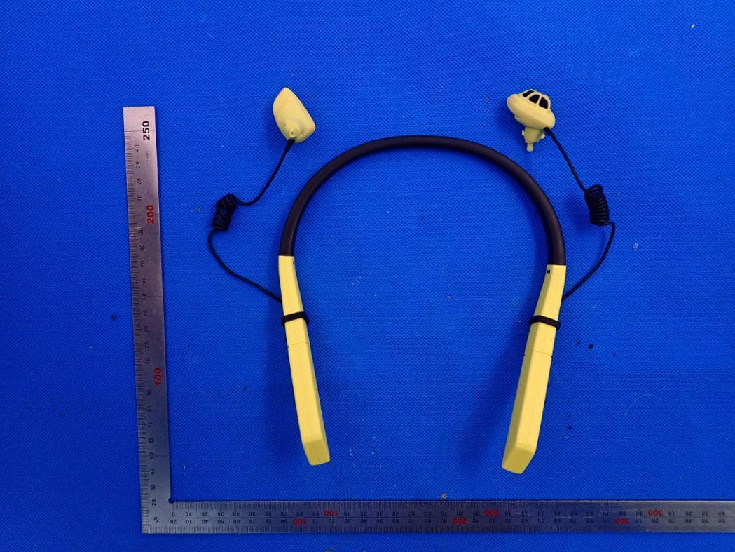
2AXCP-CLEAR360PRO
Jan 27, 2021Bluetooth Headphone
Equipment Class
DSS - Part 15 Spread Spectrum Transmitter