2AYYK-2640M1IO-Link Wireless Device Module
Kunbus GmbH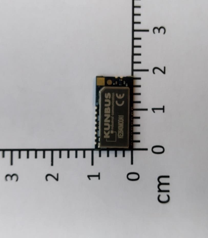
Click to zoom
Application Details
- Equipment Class
- DTS - Digital Transmission System
- Date of Grant
- May 05, 2021
- Application Purpose
- Original Equipment
- Date of Application
- May 05, 2021
- Equipment Note
- IO-Link Wireless Device Module
- Frequency Range
- 2401.00000000 - 2480.00000000
- Company
- Kunbus GmbH
- Country
- Germany
Documents & Files
Document Text
Text extracted from the exhibit documents filed with the FCC. Open a document above to read the original.
Users Manual
Data Sheet IO-Link Wireless Device Module KE2640MODA1 DO0402R01 • 4/20/2021 KUNBUS GmbHTable of Contents IO-Link Wireless Device Moduleii Table of Contents 1Disclaimer....................................................................................................................................................3 2Overview.......................................................................................................................................................4 2.1Features................................................................................................................................................4 2.2Application............................................................................................................................................4 3Certification..................................................................................................................................................5 3.1North America Statements (FCC and IC).............................................................................................5 3.2FCC and IC Modular Transmitter Instructions......................................................................................5 4Key Specification.........................................................................................................................................8 5Block Diagram.............................................................................................................................................10 6Typical Application Circuit.........................................................................................................................11 7Pin Assignment...........................................................................................................................................12 8Firmware.......................................................................................................................................................13 8.1Pre-installed Firmware..........................................................................................................................13 8.2Host Interface.......................................................................................................................................13 9Antenna Gain Setting..................................................................................................................................16 10Layout Guidelines.......................................................................................................................................17 10.1PCB Specification.................................................................................................................................17 10.2Layout...................................................................................................................................................18 11Footprint Indications...................................................................................................................................21 11.1Top View...............................................................................................................................................21 11.2Dimensions...........................................................................................................................................22 12Contact Details............................................................................................................................................23 IO-Link Wireless Device Module3 1Disclaimer © 2021 KUNBUS GmbH, Denkendorf (Germany) The contents of this document have been prepared by KUNBUS GmbH with the utmost care. Due to technical developments, KUNBUS GmbH reserves the right to change or replace the contents of this document without prior notice. You can always obtain the latest version of the user manual at our homepage: www.kunbus.de KUNBUS GmbH shall be liable exclusively to the extent specified in the General Terms and Conditions (www.kunbus.de/agb.html). The contents published in this document are protected by copyright. Any reproduction or use for the user’s in-house requirements is permitted. Reproduction or use for other purposes is not permitted without the express, written consent of KUNBUS GmbH. Contraventions shall result in compensation for damages. Trademark Protection KUNBUS is a registered trademark of KUNBUS GmbH. Disclaimer IO-Link Wireless Device Module4 2Overview KE2640MODA1 is an IO-Link Wireless system on module (SOM) that supports physical layer, data link layer and all upper layer services of the IO-Link Wireless Device as specified in the IO-Link Wireless System Extensions v1.1. The module can either be used as SOM providing the entire IO- Link Wireless Device solution on module or as communication controller for a host processor. –Integrates TI Low Energy Wireless MCU CC2640R2F to support all physical and upper layer services of an IO-Link Wireless Device –With power amplifier (PA)/low noise amplifier (LNA) to support TX Power range and RX sensi- tivity required for IO-Link Wireless system –Single-ended RF interface for external antenna –Small form factor (10 mm x 19 mm ) 2.1Features –Supply voltage: 2.0 - 3.6 V –Frequency band: 2401 – 2480 MHz –Maximum transmission power: 10 dBm –Pre-certified for compliance with the following radio frequency regulations –FCC (USA) –IC (Canada) –ETSI EN (Europe) 2.2Application –2.4 GHz low-power IO-Link Wireless systems –IO-Link Wireless Device with or without host controller –Device products (e.g. sensors or actuators) Overview IO-Link Wireless Device Module5 3Certification The KE2640MODA1 module is certified to the standards listed in the following table (with IDs where applicable). Certification BodySpecificationID FCC (USA)Title 47 CFR Part 15 + MPE2AYYK-2640M1 IC (Canada)RSS - 247 Issue 2 + RSS-102 Issue 5 (MPE)26994-2640M1 EN (Europe)ETSI EN 300 328 V2.2.2n/a 3.1N…
Text truncated - open the document above for the full version.
External Photos
KE2640MODA1 – External Fotos Property of KUNBUS GmbH Heerweg 15c, 73770 Denkendorf, Germany [email protected]
ID Label/Location Info
KE2640MODA1 – Label Information Property of KUNBUS GmbH Heerweg 15c, 73770 Denkendorf, Germany [email protected]
Internal Photos
KE2640MODA1 – Internal Fotos Property of KUNBUS GmbH Heerweg 15c, 73770 Denkendorf, Germany [email protected]
RF Exposure Info
© CTC advanced GmbH Page 1 of 3 Maximum Permissible Exposure (MPE) & Exposure evaluation Report identification number: 1-0437/20-01-09-A MPE (FCC_ISED) Certification numbers and labeling requirements FCC ID 2AYYK-2640M1 ISED number 26994-2640M1 HVIN (Hardware Version Identification Number) KE2640MODA1 PMN (Product Marketing Name) IO-Link Wireless Device Module FVIN (Firmware Version Identification Number) -/- HMN (Host Marketing Name) -/- This report is electronically signed and valid without handwriting signature. For verification of the electronic signatures, the public keys can be requested at the testing laboratory. Document authorised: p.o. Alexander Hnatovskiy Marco Scigliano Lab Manager Testing Manager Radio Communications & EMC Radio Communications & EMC Report no.: 1-0437/20-01-09-A © CTC advanced GmbH Page 2 of 3 EUT technologies: Technologies: Max. power [dBm] Antenna gain max.: [dBi] * # conducted EIRP DTS 2450 MHz decl.10.0 meas. 6.8 decl. 14.9 meas. 11.7 4.9 A Details and origins of the measurements shown in the table above: # Results from: Additional information A 1-0437/20-01-05 CTC Advanced GmbH Antenna gain page 19, Max conducted page 26 )* worst case of all antenna types, channels and modulations (overrated) Prediction of MPE limit at given distance - FCC Equation from page 18 of OET Bulletin 65, Edition 97-01 S = PG / 4 π R 2 where: S = Power density P = Power input to the antenna G = Antenna gain R = Distance to the center of radiation of the antenna PG = Output Power including antenna gain The table below is excerpted from Table 1B of 47 CFR 1.1310 titled “Limits for Maximum Permissible Exposure (MPE), Limits for General Population/Uncontrolled Exposure” Frequency Range (MHz) Power Density (mW/cm 2 ) Averaging Time (minutes) 300 -1500 f/1500 30 1500 - 100000 1.0 30 where f = Frequency (MHz) Prediction: worst case TechnologyDTS Frequency2450MHz PDeclared max power input to the antenna10dBm RDistance20cm GAntenna gain4.9dBi SMPE limit for uncontrolled exposure1.0000 mW/cm 2 Calculated Power density:0.0062mW/cm² Calculated percentage of limit:0.62% This prediction demonstrates the following: The power density levels for FCC at a distance of 20 cm are below the maximum levels allowed by regulations. Report no.: 1-0437/20-01-09-A © CTC advanced GmbH Page 3 of 3 Prediction of MPE limit at given distance - ISED RSS-102, Issue 5, 2.5.2 RF exposure evaluation is required if the separation distance between the user and/or bystander and the device’s radiating element is greater than 20 cm, except when the device operates as follows: • below 20 MHz and the source-based, time-averaged maximum e.i.r.p. of the device is equal to or less than 1 W (adjusted for tune-up tolerance); • at or above 20 MHz and below 48 MHz and the source-based, time-averaged maximum e.i.r.p. of the device is equal to or less than 4.49/ƒ 0.5 W (adjusted for tune-up tolerance), where ƒ is in MHz; • at or above 48 MHz and below 300 MHz and the source-based, time-averaged maximum e.i.r.p. of the device is equal to or less than 0.6 W (adjusted for tune-up tolerance); • at or above 300 MHz and below 6 GHz and the source-based, time-averaged maximum e.i.r.p. of the device is equal to or less than 1.31 x 10 -2 ƒ 0.6834 W (adjusted for tune-up tolerance), where ƒ is in MHz; • at or above 6 GHz and the source-based, time-averaged maximum e.i.r.p. of the device is equal to or less than 5 W (adjusted for tune-up tolerance). Prediction: worst case DTS Frequency2450MHz RDistance20cm PMax power input to the antenna10dBm GAntenna gain4.9dBi PG Maximum EIRP14.9dBm P G Maximum EIRP30.9mW Exclusion Limit from above:2.71W Calculated percentage of Limit: 1.14% Conclusion: RF exposure evaluation is not required.
Test Report
TEST REPORT Test report no.: 1-0437/20-01-05 Testing laboratory Applicant CTC advanced GmbH Untertuerkheimer Strasse 6 – 10 66117 Saarbruecken / Germany Phone: + 49 681 5 98 - 0 Fax: + 49 681 5 98 - 9075 Internet: https://www.ctcadvanced.com e-mail: [email protected] Accredited Testing Laboratory: The testing laboratory (area of testing) is accredited according to DIN EN ISO/IEC 17025 (2018-03) by the Deutsche Akkreditierungsstelle GmbH (DAkkS) The accreditation is valid for the scope of testing procedures as stated in the accreditation certificate starting with the registration number: D-PL-12076-01. KUNBUS GmbH Heerweg 15C 73770 Denkendorf / GERMANY Phone: -/- Contact: Ralf Kaptur e-mail: [email protected] Phone: +49 (711) 40091 620 Manufacturer KUNBUS GmbH Heerweg 15C 73770 Denkendorf / GERMANY Test standard/s FCC - Title 47 CFR Part 15 FCC - Title 47 of the Code of Federal Regulations; Chapter I; Part 15 - Radio frequency devices RSS - 247 Issue 2 Digital Transmission Systems (DTSs), Frequency Hopping Systems (FHSs) and Licence - Exempt Local Area Network (LE-LAN) Devices For further applied test standards please refer to section 3 of this test report. Test Item Kind of test item: IO-Link Wireless Device Module Model name: KE2640MODA1 FCC ID: 2AYYK-2640M1 IC: 26994-2640M1 Frequency: DTS band 2400 MHz to 2483.5 MHz Technology tested: IO-Link Wireless System Extensions Antenna: Onboard and external antennas Power supply: 3.3 V DC by external power supply Temperature range: -40°C to +85°C This test report is electronically signed and valid without handwritten signature. For verification of the electronic signatures, the public keys can be requested at the testing laboratory. Test report authorized: Test performed: Michael Dorongovski David Lang Lab Manager Lab Manager Radio Communications Radio Communications Test report no.: 1-0437/20-01-05 © CTC advanced GmbH Page 2 of 60 1 Table of contents 1 Table of contents ............................................................................................................................................. 2 2 General information ......................................................................................................................................... 3 2.1 Notes and disclaimer ............................................................................................................................ 3 2.2 Application details ................................................................................................................................ 3 2.3 Test laboratories sub-contracted ......................................................................................................... 3 3 Test standard/s, references and accreditations .............................................................................................. 4 4 Reporting statements of conformity – decision rule ...................................................................................... 5 5 Test environment ............................................................................................................................................. 5 6 Test item .......................................................................................................................................................... 6 6.1 General description ............................................................................................................................... 6 6.2 Additional information .......................................................................................................................... 6 7 Description of the test setup............................................................................................................................ 7 7.1 Shielded semi anechoic chamber ......................................................................................................... 8 7.2 Shielded fully anechoic chamber .......................................................................................................... 9 7.3 Radiated measurements > 18 GHz ...................................................................................................... 10 7.4 AC conducted ...................................................................................................................................... 11 7.5 Conducted measurements .................................................................................................................. 12 8 Sequence of testing ....................................................................................................................................... 13 8.1 Sequence of testing radiated spurious 9 kHz to 30 MHz ................................................................... 13 8.2 Sequence of testing radiated spurious 30 MHz to 1 GHz .................................................................. 14 8.3 Sequence of testing radiated spurious 1 GHz to 18 GHz ................................................................... 15 8.4 Sequence of testing radiated spurious above 18 GHz ....................................................................... 16 9 Measurement uncertainty .............................................................................................................................. 17 10 Summary of measurement results ............................................................................................................. 18 11 Additional comments ................................................................................................................................. 19 12 Measurement results.................................................................................................................................. 21 12.1 System gain ..................................................................................................................................... 21 12.2 Power spectral density ..…
Text truncated - open the document above for the full version.
Test Report
Measurement Results 1-0437/20-01-05_log1_conducted Test logging This addendum is electronically signed and valid without handwritten signature. For verification of the electronic signatures, the public keys can be requested at the testing laboratory. Document authorized: Michael Dorongovski Lab Manager Radio Communications CTC advanced GmbHUntertuerkheimer Strasse 6-10 66117 Saarbruecken / Germany Phone: +49 681 5 98 - 0 Fax: +49 681 5 98 - 9075 web: ctcadvanced.com e-mail: [email protected] Table of Content EUT Summary3 1. FCC Part 15.247 Maximum Peak Conducted Output Power DTS ~ Generic 2G44 2. FCC Part 15.247 Maximum Peak Conducted Output Power DTS ~ Generic 2G47 3. FCC Part 15.247 Maximum Peak Conducted Output Power DTS ~ Generic 2G410 4. FCC Part 15.247 Bandwidth 6dB DTS ~ Generic 2G413 5. FCC Part 15.247 Bandwidth 6dB DTS ~ Generic 2G415 6. FCC Part 15.247 Bandwidth 6dB DTS ~ Generic 2G417 7. FCC Part 15.247 Peak Power Spectral Density DTS ~ Generic 2G419 8. FCC Part 15.247 Peak Power Spectral Density DTS ~ Generic 2G421 9. FCC Part 15.247 Peak Power Spectral Density DTS ~ Generic 2G423 10. FCC Part 15.247 Bandwidth 99PCT-20dB ~ Generic 2G425 11. FCC Part 15.247 Bandwidth 99PCT-20dB ~ Generic 2G428 12. FCC Part 15.247 Bandwidth 99PCT-20dB ~ Generic 2G431 13. FCC Part 15.247 TX Spurious Conduced ~ Generic 2G434 14. FCC Part 15.247 TX Spurious Conduced ~ Generic 2G436 15. FCC Part 15.247 TX Spurious Conduced ~ Generic 2G438 16. FCC Part 15.247 Restricted Band Edge Conducted Avg DC corrected DTS (eirp) ~ Generic 2G440 17. FCC Part 15.247 Restricted Band Edge Conducted Avg DC corrected DTS (eirp) ~ Generic 2G443 Document No. 1-0437/20-01-05_log1_conducted2/45 EUT Summary IUT DEFINITION & Common settings Manufacturer KUNBUS GmbH TypeKE2640MODA1 Serial No. | Setup No.Device 2 | Antenna gain 0 SW Version | HW Version1.0.1 | PR100335R01 Comment 1 | 2 Tlow | Tmid | Thigh [°C] -40 | 20 | 85 Vlow | Vmid | Vhigh [V] @Imax [A] 5 | 5 | 5 @1 Auto Control enabled Power Supply | Climatic BoxNo | No Additional Path Loss [dB]0.7 IUT Common Settings 2G4 Hopping supported No Burst length [ms]10 Nominal Bandwidth [MHz]2.5 User InteractionNo Document No. 1-0437/20-01-05_log1_conducted3/45 1. FCC Part 15.247 Maximum Peak Conducted Output Power DTS ~ Generic 2G4 Test References TC Start09.12.2020 16:16:25 Ambit Temp [°C] | Humidity [rel%] 24.3 | 23 System Version1.0.1.2 Test SpecificationFCC Part 15.247 Test MethodDTS: KDB 558074 D01 V05 - Chapter 8.3.1.1 RBW ≥ DTS Bandwidth Class / TC VersionTC_VM_FCC15247_Maximum_Peak_Conducted_Output_Power_DTS_V01 Version: 0.0.1 My DescriptionFCC 15.247 Maximum Peak Output Power Conducted DTS4 - Generic 2G4 Add. Information Test Parameter Technology to testGeneric 2G4 Antenna Port used1 Temperaturemid Voltagemid Frequency low to testTrue | Freq [MHz] 2401 Frequency mid to testFalse | Freq [MHz] 2440 Frequency high to testFalse | Freq [MHz] 2480 Switched PathIUT - SignalingUnit - SpectrumAnalyzer Devices in use | SA: Rohde&Schwarz,FSV-40,1307.9002K40/101042,3.60 Document No. 1-0437/20-01-05_log1_conducted4/45 Test at TX 2401 MHz READ SA SETTINGS: RefLevel [dBm] | RefLevelOffset [dB] | InpAtt [dB]9.27 | 16.26 | 10 Start [MHz] | Stop [MHz]2398.500 | 2403.500 RBW [MHz] | VBW [MHz]0.100000 | 0.300000 Detector | TraceModePOS | MAXH Sweep: Time [ms] | Count | Points per Section | Type50 | 200 | 10001 | SWE DTS Bandwidth Test DescriptionLower LimitUpper LimitMeasuredUnitVerdict DTS Bandwidth (6dB)------729kHzINFO Plot_FCC Part 15.247 Maximum Peak Conducted Output Power DTS ~ Generic 2G4 DTS BW_09122020_161653.png READ SA SETTINGS: RefLevel [dBm] | RefLevelOffset [dB] | InpAtt [dB]14.27 | 16.26 | 15 Start [MHz] | Stop [MHz]2398.500 | 2403.500 RBW [MHz] | VBW [MHz]1.000000 | 5.000000 Detector | TraceModePOS | MAXH Sweep: Time [ms] | Count | Points per Section | Type50 | 200 | 1001 | SWE RESULT Test DescriptionLower LimitUpper LimitMeasuredUnitVerdict Peak Power---30.004.26dBmPASS Peak Power---10002.666859mWPASS Frequency at Peak------2400.72MHzINFO Document No. 1-0437/20-01-05_log1_conducted5/45 Plot_FCC Part 15.247 Maximum Peak Conducted Output Power DTS ~ Generic 2G4_09122020_161709.png TEST FINISHED General Verdict09.12.2020 16:17:09 / RT: 44 sPASS Document No. 1-0437/20-01-05_log1_conducted6/45 2. FCC Part 15.247 Maximum Peak Conducted Output Power DTS ~ Generic 2G4 Test References TC Start09.12.2020 16:25:49 Ambit Temp [°C] | Humidity [rel%] 24.3 | 23 System Version1.0.1.2 Test SpecificationFCC Part 15.247 Test MethodDTS: KDB 558074 D01 V05 - Chapter 8.3.1.1 RBW ≥ DTS Bandwidth Class / TC VersionTC_VM_FCC15247_Maximum_Peak_Conducted_Output_Power_DTS_V01 Version: 0.0.1 My DescriptionFCC 15.247 Maximum Peak Output Power Conducted DTS4 - Generic 2G4 Add. Information Test Parameter Technology to testGeneric 2G4 Antenna Port used1 Temperaturemid Voltagemid Frequency low to testFalse | Freq [MHz] 2401 Frequency mid to testTrue | Freq [MHz] 2440 Frequency high to testFalse | Freq [MHz] 2480 Switched PathIUT - SignalingUnit - SpectrumAnalyzer Devices in use | SA: Rohde&Schwarz,FSV-40,1307.9002K40/101042,3.60 Document No. 1-0437/20-01-05_log1_conducted7/45 Test at TX 2440 MHz READ SA SETTINGS: RefLevel [dBm] | RefLevelOffset [dB] | InpAtt [dB]11.73 | 16.18 | 15 Start [MHz] | Stop [MHz]2437.500 | 2442.500 RBW [MHz] | VBW [MHz]0.100000 | 0.300000 Detector | TraceModePOS | MAXH Sweep: Time [ms] | Count | Points per Section | Type50 | 200 | 10001 | SWE DTS Bandwidth Test DescriptionLower LimitUpper LimitMeasuredUnitVerdict DTS Bandwidth (6dB)------748kHzINFO Plot_FCC Part 15.247 Maximum Peak Conducted Output Power DTS ~ Generic 2G4 DTS BW_09122020_162617.png READ SA SETTINGS: RefLevel [dBm] | RefLevelOffset [dB] | InpAtt [dB]16.73 | 16.18 | 20 Start [MHz] | Stop [MHz]2437.500 | 2442.500 RBW [MHz] | VBW [MHz]1.000000 | 5.000000 Detector | TraceModePOS | MAXH Sweep: Time [ms] | Count | Points per Section | Type50 | 200 | 1001 | SWE RESULT Test DescriptionLower LimitUpper LimitMeasuredUn…
Text truncated - open the document above for the full version.
Test Report
Measurement Results 1-0437/20-01-05_log2_conducted Test logging This addendum is electronically signed and valid without handwritten signature. For verification of the electronic signatures, the public keys can be requested at the testing laboratory. Document authorized: Michael Dorongovski Lab Manager Radio Communications CTC advanced GmbHUntertuerkheimer Strasse 6-10 66117 Saarbruecken / Germany Phone: +49 681 5 98 - 0 Fax: +49 681 5 98 - 9075 web: ctcadvanced.com e-mail: [email protected] Table of Content EUT Summary3 1. FCC Part 15.247 Maximum Peak Conducted Output Power DTS ~ Generic 2G44 2. FCC Part 15.247 Maximum Peak Conducted Output Power DTS ~ Generic 2G47 3. FCC Part 15.247 Maximum Peak Conducted Output Power DTS ~ Generic 2G410 4. FCC Part 15.247 Bandwidth 6dB DTS ~ Generic 2G413 5. FCC Part 15.247 Bandwidth 6dB DTS ~ Generic 2G415 6. FCC Part 15.247 Bandwidth 6dB DTS ~ Generic 2G417 7. FCC Part 15.247 Peak Power Spectral Density DTS ~ Generic 2G419 8. FCC Part 15.247 Peak Power Spectral Density DTS ~ Generic 2G421 9. FCC Part 15.247 Peak Power Spectral Density DTS ~ Generic 2G423 10. FCC Part 15.247 Bandwidth 99PCT-20dB ~ Generic 2G425 11. FCC Part 15.247 Bandwidth 99PCT-20dB ~ Generic 2G428 12. FCC Part 15.247 Bandwidth 99PCT-20dB ~ Generic 2G431 13. FCC Part 15.247 TX Spurious Conduced ~ Generic 2G434 14. FCC Part 15.247 TX Spurious Conduced ~ Generic 2G436 15. FCC Part 15.247 TX Spurious Conduced ~ Generic 2G438 16. FCC Part 15.247 Restricted Band Edge Conducted Avg DC corrected DTS (eirp) ~ Generic 2G440 17. FCC Part 15.247 Restricted Band Edge Conducted Avg DC corrected DTS (eirp) ~ Generic 2G443 Document No. 1-0437/20-01-05_log2_conducted2/45 EUT Summary IUT DEFINITION & Common settings ManufacturerKUNBUS GmbH TypeKE2640MODA1 Serial No. | Setup No.Device 2 | Antenna gain 3 SW Version | HW Version1.0.1 | PR100335R01 Comment 1 | 2 Tlow | Tmid | Thigh [°C] -40 | 20 | 85 Vlow | Vmid | Vhigh [V] @Imax [A] 5 | 5 | 5 @1 Auto Control enabled Power Supply | Climatic BoxNo | No Additional Path Loss [dB]0.7 IUT Common Settings 2G4 Hopping supported No Burst length [ms]10 Nominal Bandwidth [MHz]2.5 User InteractionNo Document No. 1-0437/20-01-05_log2_conducted3/45 1. FCC Part 15.247 Maximum Peak Conducted Output Power DTS ~ Generic 2G4 Test References TC Start09.12.2020 15:44:08 Ambit Temp [°C] | Humidity [rel%] 24.3 | 23 System Version1.0.1.2 Test SpecificationFCC Part 15.247 Test MethodDTS: KDB 558074 D01 V05 - Chapter 8.3.1.1 RBW ≥ DTS Bandwidth Class / TC VersionTC_VM_FCC15247_Maximum_Peak_Conducted_Output_Power_DTS_V01 Version: 0.0.1 My DescriptionFCC 15.247 Maximum Peak Output Power Conducted DTS4 - Generic 2G4 Add. Information Test Parameter Technology to testGeneric 2G4 Antenna Port used1 Temperaturemid Voltagemid Frequency low to testTrue | Freq [MHz] 2401 Frequency mid to testFalse | Freq [MHz] 2440 Frequency high to testFalse | Freq [MHz] 2480 Switched PathIUT - SignalingUnit - SpectrumAnalyzer Devices in use | SA: Rohde&Schwarz,FSV-40,1307.9002K40/101042,3.60 Document No. 1-0437/20-01-05_log2_conducted4/45 Test at TX 2401 MHz READ SA SETTINGS: RefLevel [dBm] | RefLevelOffset [dB] | InpAtt [dB]5.58 | 16.26 | 5 Start [MHz] | Stop [MHz]2398.500 | 2403.500 RBW [MHz] | VBW [MHz]0.100000 | 0.300000 Detector | TraceModePOS | MAXH Sweep: Time [ms] | Count | Points per Section | Type50 | 200 | 10001 | SWE DTS Bandwidth Test DescriptionLower LimitUpper LimitMeasuredUnitVerdict DTS Bandwidth (6dB)------726kHzINFO Plot_FCC Part 15.247 Maximum Peak Conducted Output Power DTS ~ Generic 2G4 DTS BW_09122020_154437.png READ SA SETTINGS: RefLevel [dBm] | RefLevelOffset [dB] | InpAtt [dB]10.58 | 16.26 | 10 Start [MHz] | Stop [MHz]2398.500 | 2403.500 RBW [MHz] | VBW [MHz]1.000000 | 5.000000 Detector | TraceModePOS | MAXH Sweep: Time [ms] | Count | Points per Section | Type50 | 200 | 1001 | SWE RESULT Test DescriptionLower LimitUpper LimitMeasuredUnitVerdict Peak Power---30.000.59dBmPASS Peak Power---10001.145513mWPASS Frequency at Peak------2400.675MHzINFO Document No. 1-0437/20-01-05_log2_conducted5/45 Plot_FCC Part 15.247 Maximum Peak Conducted Output Power DTS ~ Generic 2G4_09122020_154453.png TEST FINISHED General Verdict09.12.2020 15:44:53 / RT: 44 sPASS Document No. 1-0437/20-01-05_log2_conducted6/45 2. FCC Part 15.247 Maximum Peak Conducted Output Power DTS ~ Generic 2G4 Test References TC Start09.12.2020 15:57:12 Ambit Temp [°C] | Humidity [rel%] 24.2 | 23 System Version1.0.1.2 Test SpecificationFCC Part 15.247 Test MethodDTS: KDB 558074 D01 V05 - Chapter 8.3.1.1 RBW ≥ DTS Bandwidth Class / TC VersionTC_VM_FCC15247_Maximum_Peak_Conducted_Output_Power_DTS_V01 Version: 0.0.1 My DescriptionFCC 15.247 Maximum Peak Output Power Conducted DTS4 - Generic 2G4 Add. Information Test Parameter Technology to testGeneric 2G4 Antenna Port used1 Temperaturemid Voltagemid Frequency low to testFalse | Freq [MHz] 2401 Frequency mid to testTrue | Freq [MHz] 2440 Frequency high to testFalse | Freq [MHz] 2480 Switched PathIUT - SignalingUnit - SpectrumAnalyzer Devices in use | SA: Rohde&Schwarz,FSV-40,1307.9002K40/101042,3.60 Document No. 1-0437/20-01-05_log2_conducted7/45 Test at TX 2440 MHz READ SA SETTINGS: RefLevel [dBm] | RefLevelOffset [dB] | InpAtt [dB]8.33 | 16.18 | 10 Start [MHz] | Stop [MHz]2437.500 | 2442.500 RBW [MHz] | VBW [MHz]0.100000 | 0.300000 Detector | TraceModePOS | MAXH Sweep: Time [ms] | Count | Points per Section | Type50 | 200 | 10001 | SWE DTS Bandwidth Test DescriptionLower LimitUpper LimitMeasuredUnitVerdict DTS Bandwidth (6dB)------744kHzINFO Plot_FCC Part 15.247 Maximum Peak Conducted Output Power DTS ~ Generic 2G4 DTS BW_09122020_155740.png READ SA SETTINGS: RefLevel [dBm] | RefLevelOffset [dB] | InpAtt [dB]13.33 | 16.18 | 15 Start [MHz] | Stop [MHz]2437.500 | 2442.500 RBW [MHz] | VBW [MHz]1.000000 | 5.000000 Detector | TraceModePOS | MAXH Sweep: Time [ms] | Count | Points per Section | Type50 | 200 | 1001 | SWE RESULT Test DescriptionLower LimitUpper LimitMeasuredUnit…
Text truncated - open the document above for the full version.
Test Report
Measurement Results 1-0437/20-01-05_log3_conducted Test logging This addendum is electronically signed and valid without handwritten signature. For verification of the electronic signatures, the public keys can be requested at the testing laboratory. Document authorized: Michael Dorongovski Lab Manager Radio Communications CTC advanced GmbHUntertuerkheimer Strasse 6-10 66117 Saarbruecken / Germany Phone: +49 681 5 98 - 0 Fax: +49 681 5 98 - 9075 web: ctcadvanced.com e-mail: [email protected] Table of Content EUT Summary3 1. FCC Part 15.247 Maximum Peak Conducted Output Power DTS ~ Generic 2G44 2. FCC Part 15.247 Maximum Peak Conducted Output Power DTS ~ Generic 2G47 3. FCC Part 15.247 Maximum Peak Conducted Output Power DTS ~ Generic 2G410 4. FCC Part 15.247 Bandwidth 6dB DTS ~ Generic 2G413 5. FCC Part 15.247 Bandwidth 6dB DTS ~ Generic 2G415 6. FCC Part 15.247 Bandwidth 6dB DTS ~ Generic 2G417 7. FCC Part 15.247 Peak Power Spectral Density DTS ~ Generic 2G419 8. FCC Part 15.247 Peak Power Spectral Density DTS ~ Generic 2G421 9. FCC Part 15.247 Peak Power Spectral Density DTS ~ Generic 2G423 10. FCC Part 15.247 Bandwidth 99PCT-20dB ~ Generic 2G425 11. FCC Part 15.247 Bandwidth 99PCT-20dB ~ Generic 2G428 12. FCC Part 15.247 Bandwidth 99PCT-20dB ~ Generic 2G431 13. FCC Part 15.247 TX Spurious Conduced ~ Generic 2G434 14. FCC Part 15.247 TX Spurious Conduced ~ Generic 2G436 15. FCC Part 15.247 TX Spurious Conduced ~ Generic 2G438 16. FCC Part 15.247 Restricted Band Edge Conducted Avg DC corrected DTS (eirp) ~ Generic 2G440 17. FCC Part 15.247 Restricted Band Edge Conducted Avg DC corrected DTS (eirp) ~ Generic 2G443 Document No. 1-0437/20-01-05_log3_conducted2/45 EUT Summary IUT DEFINITION & Common settings ManufacturerKUNBUS GmbH Type KE2640MODA1 Serial No. | Setup No.Device 2 | Antenna gain 5 SW Version | HW Version 1.0.1 | PR100335R01 Comment 1 | 2 Tlow | Tmid | Thigh [°C] -40 | 20 | 85 Vlow | Vmi…
Text truncated - open the document above for the full version.
Contact Information
Applicant
Ralf Kaptur(Product Manager)
Test Firm
cetecom advanced GmbHGerald Schmidt
Technical Specifications
| # | Rule Parts | Frequency Range | Power Output |
|---|---|---|---|
| 1 | 15C | 2.40 GHz - 2.48 GHz | 4.79 mW |
Other Applications from Kunbus GmbH
2AYYK-2640M2
May 05, 2021IO-Link Wireless Master Module
Equipment Class
DTS - Digital Transmission System