2BAMT-QZBT628-2Bluetooth module
Nebula Electronic Technology Corporation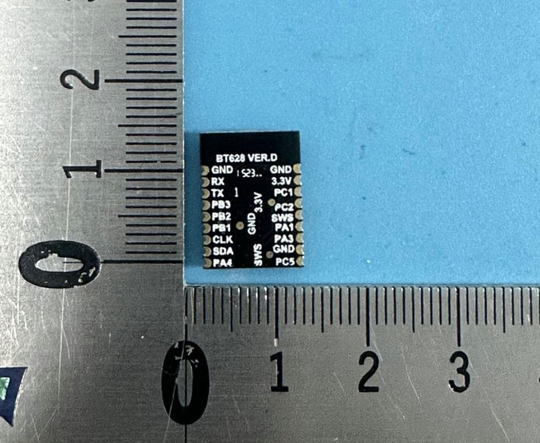
Click to zoom
Application Details
- Equipment Class
- DTS - Digital Transmission System
- Date of Grant
- Jul 30, 2023
- Application Purpose
- Original Equipment
- Date of Application
- Jul 30, 2023
- Equipment Note
- Bluetooth module
- Frequency Range
- 2402.00000000 - 2480.00000000
- Country
- China
Documents & Files
Document Text
Text extracted from the exhibit documents filed with the FCC. Open a document above to read the original.
Users Manual
1 N.E.T N.E.T 1.1GENERALDESCRIPTION QZBT628isaBLEmoduleoperatingatISMfrequencybandof2,4GHzforlow-powerwireless applications.whichisBluetooth4.2fullystandardcomplianttoalloweasyconnectivitywithBluetooth SmartReadymobilephones,tablets,laptops. TheQZBT628integratesapower-balanced32-bitproprietaryMCU,ahighperformanceBLE/2.4GHz Radio,16kBSRAM,a512kB/128kBflash,ageneral-purposeADC,aquadraturedecoder(QDEC),PWM, flexibleI/OinterfacesandotherperipheralblocksrequiredforBluetoothLowEnergyapplication development. 1.2Generalfeatures 1.BluetoothV4.2standardspecification 2.RfpowerlevelII,Ultra-lowpowerconsumption,uAworkingcurrent 3.Ultra-lowvoltagepowersupply,3VbuttonCellcanbeused 4.Multipleinterfaces:PIO/UART/AIO/I²C/SPI/PWM 5.RoHSlead-freeproductionprocessdoesnotrequireAPPfortransmission,anddatacanbedirectly transmittedtothemobilephone 6.ModuleSize15.1mm(L)*11.2mm(W) 7.TheQZBT628-1moduledoesnothaveashieldcover,andtheQZBT628-2modulehasashieldcover 1.3HardworkFeatures 1serialportand11GPIO usinghardwareflowcontrolUARTinterface,hongDebugdebugginginterface PWMforuptosixchannels 10channelADC TXOutputpower:upto+8dBm 2 N.E.T N.E.T 1.4TheconnectiondiagramofMCUandmodule Note:Thefunctionofthemodulepinscanbetocustomerneeds PB3canbesetforBluetoothexternalcontrolpin(BTC)andcancontroltheswitchofotherdevices PA4canbesettoP_SLEEP(lowpowercontrol)towakeuptheBluetoothmodule IO PB3 PA4 BTC P_SLEEP 3 N.E.T N.E.T 2.KeyElectricalSpecifications 2.1Absolutemaximumratings ItemSym.Min.MaxUnitConditions SupplyVoltageV DD -0.33.9 V AllAVDDandDVDD pinmusthavethe samevoltage VoltageoninputpinV IN -0.3V DD +0.3 V- OutputvoltageV OUT 0V DD V- StoragetemperaturerangeT Str -65150 °C - SolderingtemperatureT Sld -260 °C - 2.2Recommendedoperatingcondition ItemSym.MinTyp.MaxUnitConditions Power-supplyvoltage V DD 1.93.33.6 V - Supplyrisetime (from1.6Vto1.8V) T r --1 ms - Operatingtemperaturerange T Opr -40-85°C- 2.3DCcharacteristics (V DD =3.3V,T=25°C) ModeSym.MinTyp.MaxUnitConditions TXI Tx -14.5 - mA 0dBmContinuousTx transmission -25 - mA 8dBmContinuousTx transmission RXI Tx -16. - - mAContinuousRxreception SuspendI susp -8-μAIOwakeup -10-μATimerwakeup Deepsleep I Deep1 -1-μA Flashnotincluded, without32kHzexternal XOSC,andinternal32kHz RCOSCoff I Deep2 -1.7--μA Flashnotincluded,with 32kHzexternalXOSC, andinternal32kHzRC OSCoff I Deep3 -2.2-μA Flashnotincluded, without32kHzexternal XOSC,andinternal32kHz RCOSCon NOTE: Without32KRC:ThewakeupsourceisexternalsignalfromGPIOinput,theinternal32KRCisdisabled With32KRC:Thewakeupsourceis32KRC,itisenabled. 4 N.E.T N.E.T 3.Pinsanddescription NO. 名称描述 1,8,18GNDGND 2VCC3.3V 3 PC1 PWM2invertingoutput/GPIOPC[1] 4PC2 SPISlavechipselect(activelow)/SPIMasterchipselect(activelow)/PWM0 invertingoutput/UART_CTS/GPIOPC[2] 5 SWS Singlewireslave/PWM3output/GPIOPC[7] 6PA1PWM3invertingoutput/UART_CTS/GPIOPA[1] 7PA3PWM4output/UART_TX/I2CMasterclock/SPISlavedatainput/GPIOPA[3] 9PC5SPISlaveclock/I2CMasterclock/SPIMasterclock/UART_RX/GPIOPC[5] 10PA4 PWM2output/UART_RX/I2CMasterserialdata/SPISlaveclock/GPIOPA[4] (CanSettoP_SLEEP) 11I2C_SDA PWM4invertingoutput/I2CSlaveserialdata/I2CMasterserialdata/Control externalLNA/GPIOPA[6] 12I2C_CLKPWM5output/I2CSlaveclock/I2CMasterclock/GPIOPA[5] 13PB1PWM1output/SPIMasterdataoutput/ControlexternalPA/GPIOPB[1]/PGAinput 14PB2 PWM2output/SPIMasterdatainput/UART_CTS/I2CMasterclock/GPIOPB[2]/ PGAinput 15PB3 PWM0output/SPIMasterclock/UART_RTS/I2CMasterserialdata/GPIOPB[3] (CansettoBT_C) 16USRT_TXPWM1invertingoutput/UART_TX/GPIOPB[4]/PGAinput 17UART_RXPWM4output/UART_RX/GPIOPB[5]/PGAinput 5 N.E.T N.E.T 4.Dimension QZBT628-1 QZBT628-2 6 N.E.T N.E.T 5. Schematic 6. BOM PCB assemblyparts Part NameDescriptionQTY.UnitRemark CapacitorROHS1.8pF0201, X7R, +/-10%2C1, C2 CapacitorROHS1μF 0201 , X7R, +/-10%4C3, C6, C7, C8 InductorROHS2.2 nH 0402, +/-5%1L1 ICTelink 2.4G BluetoothIC'TLSR8232F512ET24QFN241U1 Crystal24 MHz 12 pF 20 ppM 201 6 Package1Y1 PCB ROHSDoubleside FR4 Thickness0.8mm Size:15.1mm*11.2mm 1Main PCB ShieldingcaseCopper-NickelAlloy Thickness0.2mm1 For QZBT628- 2 CONFIDENTIAL 7 N.E.T N.E.T 7.PCBLayout FCC Statement FCC standards: FCC CFR Title 47 Part 15 Subpart C Section 15.247 Device is equipped with PCB antenna , Antenna gain -6.25dBi This device complies with part 15 of the FCC Rules. Operation is subject to the following two conditions: (1) This device may not cause harmful interference, and (2) this device must accept any interference received, including interference that may cause undesired operation. Any Changes or modifications not expressly approved by the party responsible for compliance could void the user's authority to operate the equipment. Note: This equipment has been tested and found to comply with the limits for a Class B digital device, pursuant to part 15 of the FCC Rules. These limits are designed to provide reasonable protection against harmful interference in a residential installation. This equipment generates, uses and can radiate radio frequency energy and, if not installed and used in accordance with the instructions, may cause harmful interference to radio communications. However, there is no guarantee that interference will not occur in a particular installation. If this equipment does cause harmful interference to radio or television reception, which can be determined by turning the equipment off and on, the user is encouraged to try to correct the interference by one or more of the following measures: —Reorient or relocate the receiving antenna. —Increase the separation between the equipment and receiver. —Connect the equipment into an outlet on a circuit different from that to which the receiver is connected. —Consult the dealer or an experienced radio/TV technician for help. FCC Radiation Exposure Statement The modular can be installed or integrated in mobile or fix devices . This modular cannot be installed in any portable device if without further certification such as C2PC with SAR. This modular complies with FCC RF radiation exposure l…
Text truncated - open the document above for the full version.
Attestation Statements
Nebula Electronic Technology Corporation Covered Equipment Certification Attestation Letter DATE 2023.3.29 Federal Communications Commission Authorization and Evaluation Division 7435 Oakland Mills Road Columbia, MD 21046 USA ATTN.: Reviewing Engineer F CC ID: 2BAMT-QZBT628-2 Nebula Electronic Technology Corporation ("the applicant") certifies that the equipment for which authorization is sought is not "covered" equipment prohibited from receiviny an equipment authorization pur suant to section 2.903 of the FCC rules. Note: If the equipment for which the applicant seeks authorization is producen by any of the entities identified on the current Covered List, the applicant should include an explanation on why the equipment is not "covered" equipment. N ebula Electronic Technology Corporation ("the applicant") certifies that, as of the d,1te of the filing of the application, the applicant is not identified on the Covered List as ar, entity producing "covered" equipment. Signed: Printed name: Richard Yao Title: Manager Company Name: Nebula Electronic Technology Corporation Date: 2023.3.29
Attestation Statements
Nebula Electronic Technology Corporation * the applicant must designate a contact located in the United States for purposes of acting as the applicant’ s agent for service of process, regardless of whether the applicant is a domestic or foreign entity. An applicant located in the United States may designate itself as the agent for service of process. U.S. Agent Desig natio n for Serv ic e of Pro cess - Cert if ic atio n Attestatio n Letter DATE 2023.7.24 TO: Federal Communicati ons Commission 7435 Oakland Mills Road Columbia, MD 21046 ATTN.: Reviewing Engineer FCC ID:2BAMT-QZBT628-2Click here to enter text. FRN of applicant: 0033564469 Per section 2.911(d)(7) of the FCC rules, Nebula Electronic Technology Corporation(“the applicant”)certifies that the equipment for which authorization is sought is designated to the following U.S. agent* for service of process: Company Name: Baihetian Innovative Solutions FCC Registration Number (FRN): 0033401605 Physical U.S. Company Address: 6837 Chase Rd Dearborn, MI 48126 Contact Person: Kenneth Young Agent Email Address: [email protected] The above contact person accepts the obligation for service of process. The applicant accepts to maintain an agent for no less than one year after the grantee has terminated all marketing and importation or the conclusion of any Commission-related proceeding involving the equipment. Applicant Signed: Signed: Printed name:RichardYao Title: Manager Company Name: Nebula Electronic Technology Corporation Date: 2023.7.214 Agent Signed (if different from Applicant): Signed: Printed name:Kenneth Young Title: Manager Company Name: Baihetian Innovative Solutions Date: 2023.5.6
Cover Letter(s)
Compliance list INTEGRATION INSTRUCTIONS for 996369 D03 OEM the and 996369 D03 OEM by Sections 2.2 through 2.10. Requirement Yes N/A Comment 2.2 List of applicable FCC rules List the FCC rules that are applicable to the modular transmitter. These are the rules that specifically establish the bands of operation, the power, spurious emissions, and operating fundamental frequencies. DO NOT list compliance to unintentional-radiator rules (Part 15 Subpart B) since that is not a condition of a module grant that is extended to a host manufacturer. See also Section 2.10 below concerning the need to notify host manufacturers that further testing is required.3 YES Refer to instruction FCC standards: FCC CFR Title 47 Part 15 Subpart C Section 15.247 2.3 Summarize the specific operational use conditions Describe use conditions that are applicable to the modular transmitter, including for example any limits on antennas, etc. For example, if point-to-point antennas are used that require reduction in power or compensation for cable loss, then this information must be in the instructions. If the use condition limitations extend to professional users, then instructions must state that this information also extends to the host manufacturer’s instruction manual. In addition, certain information may also be needed, such as peak gain per frequency band and minimum gain, specifically for master devices in 5 GHz DFS bands. YES Refer to instruction Device is equipped with PCB antenna , Antenna gain -6.25dBi 2.4 Limited module procedures If a modular transmitter is approved as a “limited module,” then the module manufacturer is responsible for approving the host environment that the limited module is used with. The manufacturer of a limited module must describe, both in the filing and in the installation instructions, the alternative means that the limited module manufacturer uses to verify that the host meets the necessary requirements to satisfy the module limiting conditions. A limited module manufacturer has the flexibility to define its alternative method to address the conditions that limit the initial approval, such as: shielding, minimum N/A Not applicable signaling amplitude, buffered modulation/data inputs, or power supply regulation. The alternative method could include that the limited module manufacturer reviews detailed test data or host designs prior to giving the host manufacturer approval. This limited module procedure is also applicable for RF exposure evaluation when it is necessary to demonstrate compliance in a specific host. The module manufacturer must state how control of the product into which the modular transmitter will be installed will be maintained such that full compliance of the product is always ensured. For additional hosts other than the specific host originally granted with a limited module, a Class II permissive change is required on the module grant to register the additional host as a specific host also approved with the module. 2.5 Trace antenna designs For a modular transmitter with trace antenna designs, see the guidance in Question 11 of KDB Publication 996369 D02 FAQ – Modules for Micro-Strip Antennas and traces. The integration information shall include for the TCB review the integration instructions for the following aspects: layout of trace design, parts list (BOM), antenna, connectors, and isolation requirements.4 a) Information that includes permitted variances (e.g., trace boundary limits, thickness, length, width, shape(s), dielectric constant, and impedance as applicable for each type of antenna); b) Each design shall be considered a different type (e.g., antenna length in multiple(s) of frequency, the wavelength, and antenna shape (traces in phase) can affect antenna gain and must be considered); c) The parameters shall be provided in a manner permitting host manufacturers to design the printed circuit (PC) board layout; d) Appropriate parts by manufacturer and specifications; e) Test procedures for design verification; and f) Production test procedures for ensuring N/A Not applicable compliance. The module grantee shall provide a notice that any deviation(s) from the defined parameters of the antenna trace, as described by the instructions, require that the host product manufacturer must notify the module grantee that they wish to change the antenna trace design. In this case, a Class II permissive change application is required to be filed by the grantee, or the host manufacturer can take responsibility through the change in FCC ID (new application) procedure followed by a Class II permissive change application. 2.6 RF exposure considerations It is essential for module grantees to clearly and explicitly state the RF exposure conditions that permit a host product manufacturer to use the module. Two types of instructions are required for RF exposure information: (1) to the host product manufacturer, to define the application conditions (mobile, portable – xx cm from a person’s body); and (2) additional text needed for the host product manufacturer to provide to end users in their end-product manuals. If RF exposure statements and use conditions are not provided, then the host product manufacturer is required to take responsibility of the module through a change in FCC ID (new application). YES Refer to instruction The modular can be installed or integrated in mobile or fix devices . This modular cannot be installed in any portable device if without further certification such as C2PC with SAR. This modular complies with FCC RF radiation exposure limits set forth for an uncontrolled environment. This transmitter must not be co-located or operating in conjunction with any other antenna or transmitter. This modular must be installed and operated with a minimum distance of 20 cm between the radiator and user body. 2.7 Antennas A list of antennas included in the application for certification must be provided in the instructions. For modular transmitters approved as …
Text truncated - open the document above for the full version.
Cover Letter(s)
Single Modular approval Declaration letter We, Nebula Electronic Technology Corporation applies single modular approval for Product Name: Bluetooth module Model: QZBT628-2 FCC /D:2BAMT-QZBT628-2 According to 996369 DOJ Module Equip Auth Guide v0Jr04 and 15.212 requirem�nt: 1) The radio elements must have the radio frequency circuitry shielded. Physical components and tuning capacitor(s) may be located external to the shield, but musr ?e on the module assembly; Answer: Yes 2) The module must have buffered modulation/data inputs to ensure that the device willcomply with Part 15 requirements with any type of input signal; Answer: Yes; All inputs to the modules are buffered through logic or microprocessor inputs. 3) The modular transmitter must have its own power supply regulation. A nswer: Yes; A low drop out regulator is used for modular power supply regulation. 4) The module must contain a permanently attached antenna, or contain a unique antennaconnector, and be marketed and operated only with specific antenna(s), per Sections15.203, 15.204(b), 15.204(c), 15.212(a), 2.929(b); Answer: Yes; Device is equipped with PCB antenna. (5) The module must demonstrate compliance in a stand-alone configuration; Answer: Yes? distance between modular and all AEs are bigger than 1 Ocm, refer to setup photo. (6) The module must be labeled with its permanently affixed FCC ID label, or use ::m e lectronic display (See KDB Publication 784748 about labeling requirement s); An swer: Yes ; The modular has a permanent fixed label, and below statement was listed in the User Manual; The host device must be l abeled t o disp lay th e FCCID of the module Co ntains FCC ID: 2BAMT-QZBT628-2 (7) The module must comply with all specific rules applicable to the transmitter including all the conditions provided in the in tegration instructions by the grantee; Answer: Yes; The module comply with all specifi c rules applicable to the transmitter including a ll the conditions provided in the integration instructions by t he grantee, Refer to test report and user manual . (8) The module must comply with RF exposure requirements Answer: Yes; Transmitter meets MP E calculation of 47 CFR 1.1307. Refer to MP E Reports and Refer to modular installation manual. Please contact me if you have any further questions. Thanks for your attention. Best Regards, <Signatur e > l\j e, �,J, �(} · Title: Manager Company: Nebula Electronic Technology Corporation
External Photos
Model: QZBT628-2
Internal Photos
Model: QZBT628-2
RF Exposure Info
Page 1 of 8 BlueAsia of Technical Services(Shenzhen) Co.,Ltd. Add: Building C, No. 107, Shihuan Road, Shiyan Sub-District, Baoan District, Shenzhen, Guangdong Province, China Tel: +86-755-23059481 Email: [email protected] www.cblueasia.com TEST REPORT Product Name : Bluetooth module Brand Mark : N.E.T Model No. : QZBT628-2 FCC ID : 2BAMT-QZBT628-2 Report Number : BLA-EMC-202306-A2303 Date of Sample Receipt : 2023/6/5 Date of Test : 2023/6/6 to 2023/7/7 Date of Issue : 2023/7/10 Test Standard : 47 CFR Part 15, Part1.1307 47 CFR Part 15, Part2.1093 KDB447498D04 General RF Exposure Guidance v01 Test Result : Pass Prepared for: Nebula Electronic Technology Corporation Room 1002, No.570 ShengXia RD, Pudong district, Shanghai, China Prepared by: BlueAsia of Technical Services(Shenzhen) Co.,Ltd. Building C, No. 107, Shihuan Road, Shiyan Sub-District, Baoan District, Shenzhen, Guangdong Province, China TEL: +86-755-23059481 Compiled by: Review by: Approved by: Date: 2023/7/10 Report No.: BLA-EMC-202306-A2302 Page 2 of 8 BlueAsia of Technical Services(Shenzhen) Co., Ltd. Tel: +86-755-23059481 Email: [email protected] www.cblueasia.com REPORT REVISE RECORD Version No. Date Description 00 2023/7/10 Original Report No.: BLA-EMC-202306-A2302 Page 3 of 8 BlueAsia of Technical Services(Shenzhen) Co., Ltd. Tel: +86-755-23059481 Email: [email protected] www.cblueasia.com TABLE OF CONTENTS 1 TEST SUMMARY .............................................................................................................................................. 4 2 GENERAL INFORMATION ............................................................................................................................... 5 3 GENERAL DESCRIPTION OF E.U.T. ............................................................................................................... 5 4 LABORATORY LOCATION .............................................................................................................................. 6 5 RF EXPOSURE COMPLIANCE REQUIREMENT ............................................................................................ 7 5.1 STANDARD REQUIREMENT ................................................................................................................................................. 7 5.2 LIMITS ........................................................................................................................................................................... 7 Report No.: BLA-EMC-202306-A2302 Page 4 of 8 BlueAsia of Technical Services(Shenzhen) Co., Ltd. Tel: +86-755-23059481 Email: [email protected] www.cblueasia.com 1 TEST SUMMARY Test item Test Requirement Test Method Class/Severity Result RF Exposure 47 CFR Part 1.1307, Part 2.1093, KDB 447498 CFR 47 Part 2.1093 CFR 47 Part 2.1093 PASS Report No.: BLA-EMC-202306-A2302 Page 5 of 8 BlueAsia of Technical Services(Shenzhen) Co., Ltd. Tel: +86-755-23059481 Email: [email protected] www.cblueasia.com 2 GENERAL INFORMATION Applicant Nebula Electronic Technology Corporation Address Room 1002, No.570 ShengXia RD, Pudong district, Shanghai, China Manufacturer Nebula Electronic Technology Corporation Address Room 1002, No.570 ShengXia RD, Pudong district, Shanghai, China Factory Nebula Electronic Technology Corporation Address Room 1002, No.570 ShengXia RD, Pudong district, Shanghai, China Product Name Bluetooth module Test Model No. QZBT628-2 3 GENERAL DESCRIPTION OF E.U.T. Hardware Version N/A Software Version N/A Operation Frequency: 2402MHz-2480MHz Modulation Type: GFSK Channel Spacing: 2MHz Number of Channels: 40 Antenna Type: PCB Antenna Antenna Gain: -6.25dBi(Provided by the customer) Report No.: BLA-EMC-202306-A2302 Page 6 of 8 BlueAsia of Technical Services(Shenzhen) Co., Ltd. Tel: +86-755-23059481 Email: [email protected] www.cblueasia.com 4 LABORATORY LOCATION All tests were performed at: BlueAsia of Technical Services(Shenzhen) Co.,Ltd. Building C, No. 107, Shihuan Road, Shiyan Sub-District, Baoan District, Shenzhen, Guangdong Province, China Telephone: TEL: +86-755-28682673 FAX: +86-755-28682673 No tests were sub-contracted. Report No.: BLA-EMC-202306-A2302 Page 7 of 8 BlueAsia of Technical Services(Shenzhen) Co., Ltd. Tel: +86-755-23059481 Email: [email protected] www.cblueasia.com 5 RF EXPOSURE COMPLIANCE REQUIREMENT 5.1 STANDARD REQUIREMENT According to 447498 D04 Interim General RF Exposure Guidance v01 Standalone SAR test exclusion considerations Unless specifically required by the published RF exposure KDB procedures, standalone 1-g head or body and 10-g extremity SAR evaluation for general population exposure conditions, by measurement or numerical simulation, is not required when the corresponding SAR Exclusion Threshold condition, listed below, is satisfied. 5.2 LIMITS Report No.: BLA-EMC-202306-A2302 Page 8 of 8 BlueAsia of Technical Services(Shenzhen) Co., Ltd. Tel: +86-755-23059481 Email: [email protected] www.cblueasia.com EIRP = pt×gt = (E×d)2/30 where: pt = transmitter output power in watts, gt = numeric gain of the transmitting antenna (unitless), E = electric field strength in V/m, --- 10((dBuV/m)/20)/106 d = measurement distance in meters (m)---3m Sopt = (E×d)2/30 × gt Ant gain = -6.25dBi Max Output power =5.048dBm @2480MHz ERP = 5.048dBm-6.25dBi-2.15=-3.352dBm So worse case: 10^0.5048=3.197mW < 3060 mW Comply with RF exposure exemption limit. ----END OF REPORT---- The test report is effective only with both signature and specialized stamp, The result(s) shown in this report refer only to the sample(s) tested. Without written approval of BlueAsia, this report can’t be reproduced except in full.
Test Report
Page 1 of 60 BlueAsia of Technical Services(Shenzhen) Co.,Ltd. Add: Building C, No. 107, Shihuan Road, Shiyan Sub-District, Baoan District, Shenzhen, Guangdong Province, China Tel: +86-755-23059481 Email: [email protected] www.cblueasia.com TEST REPORT Product Name : Bluetooth module Brand Mark : N.E.T Model No. : QZBT628-2 FCC ID : 2BAMT-QZBT628-2 Report Number : BLA-EMC-202306-A2301 Date of Sample Receipt : 2023/6/5 Date of Test : 2023/6/6 to 2023/7/7 Date of Issue : 2023/7/10 Test Standard : 47 CFR Part 15, Subpart C 15.247 Test Result : Pass Prepared for: Nebula Electronic Technology Corporation Room 1002, No.570 ShengXia RD, Pudong district, Shanghai, China Prepared by: BlueAsia of Technical Services(Shenzhen) Co.,Ltd. Building C, No. 107, Shihuan Road, Shiyan Sub-District, Baoan District, Shenzhen, Guangdong Province, China TEL: +86-755-23059481 Compiled by: Review by: Approved by: Date: 2023/7/10 Report No.: BLA-EMC-202306-A2301 Page 2 of 60 BlueAsia of Technical Services(Shenzhen) Co., Ltd. Tel: +86-755-23059481 Email: [email protected] www.cblueasia.com REPORT REVISE RECORD Version No. Date Description 00 2023/7/10 Original Report No.: BLA-EMC-202306-A2301 Page 3 of 60 BlueAsia of Technical Services(Shenzhen) Co., Ltd. Tel: +86-755-23059481 Email: [email protected] www.cblueasia.com TABLE OF CONTENTS 1 TEST SUMMARY .............................................................................................................................................. 5 2 GENERAL INFORMATION ............................................................................................................................... 6 3 GENERAL DESCRIPTION OF E.U.T. ............................................................................................................... 6 4 TEST ENVIRONMENT ...................................................................................................................................... 7 5 TEST MODE ...................................................................................................................................................... 7 6 MEASUREMENT UNCERTAINTY .................................................................................................................... 7 7 DESCRIPTION OF SUPPORT UNIT ................................................................................................................ 8 8 LABORATORY LOCATION .............................................................................................................................. 8 9 TEST INSTRUMENTS LIST .............................................................................................................................. 9 10 ANTENNA REQUIREMENT .......................................................................................................................... 11 10.1 CONCLUSION .............................................................................................................................................................. 11 11 CONDUCTED SPURIOUS EMISSIONS ....................................................................................................... 12 11.1 LIMITS ..................................................................................................................................................................... 12 11.2 BLOCK DIAGRAM OF TEST SETUP ............................................................................................................................ 13 11.3 TEST DATA ................................................................................................................................................................ 13 12 RADIATED SPURIOUS EMISSIONS ........................................................................................................... 14 12.1 LIMITS ..................................................................................................................................................................... 14 12.2 BLOCK DIAGRAM OF TEST SETUP ............................................................................................................................ 15 12.3 PROCEDURE ............................................................................................................................................................ 15 12.4 TEST DATA ................................................................................................................................................................ 17 13 RADIATED EMISSIONS WHICH FALL IN THE RESTRICTED BANDS ..................................................... 25 13.1 LIMITS ..................................................................................................................................................................... 25 13.2 BLOCK DIAGRAM OF TEST SETUP ............................................................................................................................ 26 13.3 PROCEDURE ............................................................................................................................................................ 26 13.4 TEST DATA ................................................................................................................................................................ 28 14 CONDUCTED BAND EDGES MEASUREMENT ......................................................................................... 32 14.1 LIMITS ..................................................................................................................................................................... 32 14.2 BLOCK DIAGRAM OF TEST SETUP ............................................................................................................................ 33 14.3 TEST DATA .............................................................................................................................................................…
Text truncated - open the document above for the full version.
Test Report
ANTENNA PASSIVE TEST REPORT Applicant Nebula Electronic Technology Corporation Manufacturer Nebula Electronic Technology Corporation Product Name BT628 BLE Module Model No QZBT628-2 Date Initial Sample(s) Received 2023-05-27 Testing Date 2023-05-27 TABLE OF CONTENTS 1.GENERAL INFORMATION .............................................................. 3 1.1 DETAILS OF CLIENT .................................................................... 3 1.2 GENERAL DESCRIPTION OF EUT ............................................... 4 1.3 LABORATORY ENVIRONMENT .................................................... 4 2. OTA MEASUREMENTS SYSTEM CONFIGURATION ...................... 5 2.1 TEST CONFIGURATION ................................................................. 5 2.2 TEST MEASUREMENT .................................................................... 5 3.TEST EQUIPMENT LIST .................................................................. 6 4.MEASUREMENT UNCERTAINTY ................................................... …
Text truncated - open the document above for the full version.
Contact Information
Applicant
Richard Yao
Test Firm
BlueAsia of Technical Services (Shenzhen)Blue Zheng
[email protected]+86 755-23059481-815
Technical Specifications
| # | Rule Parts | Frequency Range | Power Output |
|---|---|---|---|
| 1 | 15C | 2.40 GHz - 2.48 GHz | 3.20 mW |
Other Applications from Nebula Electronic Technology Corporation
2BAMT-BT829-2
Apr 09, 2023BLE module
Equipment Class
DTS - Digital Transmission System