2BAUM-M04Find My Tag
Shenzhen kingminson Electronic Co., Ltd.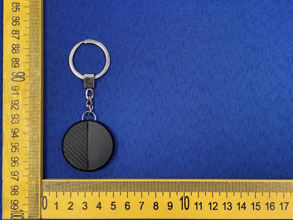
Click to zoom
Application Details
- Equipment Class
- DTS - Digital Transmission System
- Date of Grant
- Jun 26, 2023
- Application Purpose
- Original Equipment
- Date of Application
- Jun 26, 2023
- Equipment Note
- Find My Tag
- Frequency Range
- 2402.00000000 - 2480.00000000
- Country
- China
Documents & Files
Document Text
Text extracted from the exhibit documents filed with the FCC. Open a document above to read the original.
Users Manual
MOYAGOA Findmy Product Instruction 1. Product overview 2. Quick instructions 1、Turn on the device: press and hold the button for 5 seconds, the device will beep and turn on. (How to confirm whether the device has been turned on: double-click the device button, the device will sound, which means that the device has been turned on, and there is no need to restart it) 2、Open the APP that comes with the Apple mobile phone system: Find my; 3、Choose:Items; 4、Choose:Add New Item; 5、Choose:Other Supported Item; 6、During the Searching Items process, a device with the word M04 will appear; 7、Click on the device found in the APP and name it。 8、After naming, you can use device functions: A. Ring the device, click Play Sound, and the device will emit music .B. Findmy network helps to find: When the device leaves the Bluetooth distance, it cannot be connected in the APP. You can choose Lost Mode,, Enable. Enter the contact mobile phone number, etc. If there is an iPhone near the lost device, the owner’s Findmy APP can receive notifications and the latest location. 9. Delete device: To delete the device in the APP, you can select Remove item. 10、After removing the device, the device will not shut down and is in the pairing state. If there is no re-pairing within 10 minutes, the device will leave the pairing state. If you need to pair a device at this time, you need to click the device button once, the device will sound, and the light will flash once. At this time, the device enters the pairing state and can be paired with the APP again. 3. Instructions for device operation 1. Install the battery: Install the battery on the device first time, the device will enter shutdown sleep mode. When the device is in shutdown sleep mode, install the battery again, the device will enter shutdown sleep mode. When the device is in turned on mode, install the battery again, the device will enter turned on mode. 2. Device enters turned on mode from shutdown sleep mode: After install the battery in the device, if the device is in shutdown sleep mode, press and hold the button for five seconds, the device play a “turned on” sound and the led blink three times, the device is turned on. 3. Device status confirmation: Double-click the device button twice, the device play a “working” sound, and the led blink three times, indicating that the device is in turned on mode. If the device does not sound, the device is in shutdown sleep mode. Press and hold the button for five seconds to turn on. 4. Pairing mode timeout, the device enters the pairing mode again: After removing the device in the app, the device will paly a sound and the led blinks six times, it will not shut down and is in the pairing mode. If there is no re-pairing within 10 minutes, the device will leave the pairing mode (the device cannot be paired with the Find My APP at this time). If you need to pair the device, you need to click the device button once, the device will paly a “re-pairing” sound, and the led will blink once. At this time, the device enters the pairing mode and can be paired with the Find My APP again. 5. How to perform serial number lookup: Long press the device button for 3 seconds, the device led blink six times, put the device into a serial number read state. 6. Factory Reset: When the device is turned on, double-click the device button (paly a “working” sound and the led blink three times), then press and hold the device button within three seconds, after 2 seconds there will be a "beep, beep, beep" sound and the LED will blink, (don’t release), continue to press and hold the button for about eight seconds, until the device paly a “Factory Reset” sound and the led blink three times, release the button. At this time, factory reset is completed. 7. Device enters shutdown sleep mode from turned on mode: When device is in turned on mode, press the device button 5 times in 2 seconds, the device plays a “shutdown” sound and the led blink three times, the device enters shutdown sleep mode. Note: 1、 TCP005 MaxConnection is 2。 2、 For TCB002, step 7, whether the accessory will respond with an invalid state error or not respond at all if the Firmware Update characteristic is written to while the accessory is connected to a non-owner? “ The accessory will respond with an ATT error (BT_ATT_ERR_WRITE_NOT_PERMITTED) if the non-owner writes to the Firmware Update characteristic. Essentially, it means that only the owner can perform the DFU.” This device complies with part 15 of the FCC Rules. Operation is subject to the following two conditions: (1) This device may not cause harmful interference, and (2) this device must accept any interference received, including interference that may cause undesired operation. Any changes or modifications not expressly approved by the party responsible for compliance could void the user's authority to operate the equipment. NOTE: This equipment has been tested and found to comply with the limits for a Class B digital device, pursuant to Part 15 of the FCC Rules. These limits are designed to provide reasonable protection against harmful interference in a residential installation. This equipment generates, uses and can radiate radio frequency energy and, if not installed and used in accordance with the instructions, may cause harmful interference to radio communications. However, there is no guarantee that interference will not occur in a particular installation. If this equipment does cause harmful interference to radio or television reception, which can be determined by turning the equipment off and on, the user is encouraged to try to correct the interference by one or more of the following measures: -- Reorient or relocate the receiving antenna. -- Increase the separation between the equipment and receiver. -- Connect the equipment into an outlet on a circuit different from that to which the receiver is connected. -- Consult the dealer or an experienced radio/TV technician for help. The device has been evaluated to mee…
Text truncated - open the document above for the full version.
Attestation Statements
Shenzhen kingminson Electronic Co., Ltd. Federal Communications Commission Authorization and Evaluation Division 7435 Oakland Mills Road Columbia, MD 21046 USA Date: 2023-6-26 FCC ID: 2BAUM-M04 Ref. #1: Attestation Statements Part 2.911(d)(5)(i) Filing Shenzhen kingminson Electronic Co., Ltd. certifies that the equipment for which authorization is sought is not “covered” equipment prohibited from receiving an equipment authorization pursuant to section 2.903 of the FCC rules. Ref. #2: Attestation Statements Part 2.911(d)(5)(ii) Filing Shenzhen kingminson Electronic Co., Ltd. certifies that, as of the date of the filing of the application, the applicant is not identified on the Covered List as an entity producing “covered” equipment. Applicant: Shenzhen kingminson Electronic Co., Ltd. Address: 4F, Building A, Ao'de Industrial Park, Gongming Town, Guangming New District, Shenzhen, Guangdong Contact Person: Jon Zheng Tel.: +86 18665803259 Email: [email protected] Sincerely, Signature:
Attestation Statements
Effective Date: April 2, 2020 QSF 7.6.4-8 – Agent Authorization Letter Template Page 1 of 1 Revision Date: Revision: 0 Shenzhen kingminson Electronic Co., Ltd. Date:Jun 25, 2023 Product Model Number: M04, M04A, M04B, M05, M06, M07, M08 FCC ID:2BAUM-M04 To whom it may concern, Re: Product Certification Representative Authorization Letter We authorize QAI Laboratories Ltd. 3980 North Fraser Way, Burnaby B.C. Canada V5J 5K5 to act on our behalf on all matters concerning the above named equipment. This shall include the following: Testing Approval applications and procedures We declare that ORGANIZATION. is allowed to forward all information related to the approval project to the applied certification body and to the notification entities and to discuss any issues concerning the approval application. Any and all acts carried out by ORGANIZATION. on our behalf shall have the same effect as acts of our own. By: Contact Listed on FCC Wesbite Title: Manager Email: [email protected] Telephone: +86 18665803259 On behalf of: Shenzhen kingminson Electronic Co., Ltd.
Cover Letter(s)
Family models declaration letter Jun 25, 2023 We Shenzhen kingminson Electronic Co., Ltd. Of 4F, Building A, Ao'de Industrial Park, Gongming Town, Guangming New District, Shenzhen, Guangdong Declare under our sole responsibility that the product Product: Find My Tag Model Number: M04A, M04B, M05, M06, M07, M08 All the models are the same circuit and RF module, except the model No.. Thanks Sincerely, Qian yang/ Manager E-mail: : [email protected] Phone: +18665803259 Fax: 0755-29161390 Address : 4F, Building A, Ao'de Industrial Park, Gongming Town, Guangming New District, Shenzhen, Guangdong
Cover Letter(s)
Shenzhen kingminson Electronic Co., Ltd. Office of Engineering Technology Federal Communications Commission 7435 Oakland Mills Road Columbia, MD 21046 USA Date: June 25, 2023 Subject; Request for Confidentiality FCC ID: 2BAUM-M04 To Whom It May Concern, Pursuant to the provisions of the Commission’s rules Title 47 Sections §0.457 and §0.459, we are requesting the Commission to withhold the following attachment(s) as confidential documents from public disclosure indefinitely. These documents contain detailed system and equipment descriptions and are considered as proprietary information in operation of the equipment. The public disclosure of these documents might be harmful to our company and would give competitors an unfair advantage in the market. Schematic Diagram Block Diagram Parts List Operational Description Tune-up Procedure Software Security Requirements for UNII devices In additional to above mentioned documents, in order to comply with the marketing regulations in Title 47 CFR §2.803 and the importation rules in Title 47 CFR §2.1204, while ensuring that business sensitive information remains confidential until the actual marketing of newly authorized devices, we request Short Term Confidentiality of the following attachment(s); External Photos Test Setup Photos Internal Photos User Manual For 45 days, pursuant to Public Notice DA 04-1705. OR For 180 days pursuant to KDB 726920 D01. It is our understanding that all measurement test reports, FCC ID label format and correspondence during the certification review process cannot be granted as confidential documents and this information will be available for public review once the grant of equipment authorization is issued. Sincerely, Signature: Name: Jon Zheng Title: Manager
Cover Letter(s)
Design Note DN0007 2.4 GHz Inverted F Antenna By Audun Andersen Keywords •CC2400 •CC2420 •CC2430 •CC2431 •CC2500 •CC2510 •CC2511 •CC2550 •CC2520 •CC2480 •PCB Antenna •2.4 GHz •Inverted F Antenna 1 Introduction This document describes a PCB antenna design that can be used with all 2.4 GHz transceivers and transmitters from Texas Instruments. Maximum gain is measured to be +3.3 dB and overall size requirements for this antenna are 11 x 4 mm. Thus, this is a compact, low cost and high performance antenna. SWRU120B Page 1 of 14 Design Note DN0007 Table of Contents KEYWORDS.............................................................................................................................. 1 1 INTRODUCTION............................................................................................................. 1 2 ABBREVIATIONS........................................................................................................... 2 3 DESCRIPTION OF THE INVERTED F ANTENNA DESIGN ......................................... 3 3.1 IMPLEMENTATION OF THE INVERTED F ANTENNA.......................................................... 3 4 RESULTS........................................................................................................................4 4.1 RADIATION PATTERN.................................................................................................. 4 4.2 REFLECTION............................................................................................................ 11 4.3 BANDWIDTH............................................................................................................. 11 5 CONCLUSION .............................................................................................................. 12 6 REFERENCES .............................................................................................................. 13 7 GENERAL INFORMATION .......................................................................................... 14 7.1 DOCUMENT HISTORY................................................................................................ 14 2 Abbreviations CC2480 Z-Accel ZigBee Processor EM Evaluation Module IFA Inverted F Antenna ISM Industrial, Scientific, Medical PCB Printed Circuit Board SWRU120B Page 2 of 14 Design Note DN0007 3 Description of the Inverted F Antenna Design Since the impedance of the Inverted F Antenna is matched directly to 50 ohm no external matching components are needed. 3.1 Implementation of the Inverted F Antenna It is important to make an exact copy of the antenna dimensions to obtain optimum performance. The easiest approach to implement the antenna in a PCB CAD tool is to import the antenna layout from either a gerber or DXF file. Such files are included in CC2430DB reference design [1]. The gerber file is called “Inverted_F_Antenna.spl” and the DXF file is called “Inverted_F_Antenna.dxf”. If the antenna is implemented on a PCB that is wider than the antenna it is important to avoid placing components or having a ground plane close to the end points of the antenna. If the CAD tool being used doesn’t support import of gerber or DXF files, Figure 1 and Table 1 can be used. Figure 1. IFA Dimensions H1 5.70 mmW2 0.46 mm H2 0.74 mmL1 25.58 mm H3 1.29 mmL2 16.40 mm H4 2.21 mmL3 2.18 mm H5 0.66 mmL4 4.80 mm H6 1.21 mmL5 1.00 mm H7 0.80 mmL6 1.00 mm H8 1.80 mmL7 3.20 mm H9 0.61 mmL8 0.45 mm W1 1.21 mm Table 1. IFA Dimensions Since there is no ground plane beneath the antenna, PCB thickness will have little effect on the performance. The results presented in this design note are based on an antenna implemented on a PCB with 1 mm thickness. SWRU120B Page 3 of 14 Design Note DN0007 4 Results All results presented in this chapter are based on measurements performed with CC2430DB [1]. 4.1 Radiation Pattern Figure 2 shows how to relate all the radiation patterns to the orientation of the antenna. The radiation patterns were measured with CC2430 programmed to 0 dBm output power. XY plane XZ plane YZ plane Figure 2. How to Relate the Antenna to the Radiation Patterns SWRU120B Page 4 of 14 Design Note DN0007 Figure 3. XY Plane Vertical Polarization SWRU120B Page 5 of 14 Design Note DN0007 Figure 4. XY Plane Horizontal Polarization SWRU120B Page 6 of 14 Design Note DN0007 Figure 5. XZ Plane Vertical Polarization SWRU120B Page 7 of 14 Design Note DN0007 Figure 6. XZ Plane Horizontal Polarization SWRU120B Page 8 of 14 Design Note DN0007 Figure 7. YZ Plane Vertical Polarization SWRU120B Page 9 of 14 Design Note DN0007 Figure 8. YZ Plane Horizontal Polarization SWRU120B Page 10 of 14 Design Note DN0007 4.2 Reflection Figure 9. Measured Reflection at the Feed Point of the Antenna Figure 9 show that the IFA ensures less than 10 % reflection of the available power for a bandwidth of more than 300 MHz. A large bandwidth makes the antenna less sensitive to detuning due to plastic encapsulation or other objects in the vicinity of the antenna. 4.3 Bandwidth Another way of measuring the bandwidth after the antenna is implemented on a PCB and connected to a transmitter is to write test software that steps a carrier across the frequency band of interest. By using the “Max hold” function on a spectrum analyzer the variation in output power across frequency can easily be measured. Figure 10 shows how the output power varies on the IFA when the PCB is horizontally oriented and the receiving antenna has horizontal polarization. This measurement was not performed in an anechoic chamber thus the graph shows only the relative variation for the given frequency band. SWRU120B Page 11 of 14 Design Note DN0007 Bandwidth IFA 2.4 2.4835 -60 -50 -40 -30 -20 -10 0 2.22.32.42.52.62.72.8 Frequency [GHz] Relative output power [dB] Output pow er Low er band edge Upper band edge Figure 10. Bandwidth of IFA 5 Conclusion The PCB antenna presented in this document performs well for all frequencies in the 2.4 GHz ISM band. Except for two narrow …
Text truncated - open the document above for the full version.
External Photos
Ext Photos Model: Find My Tag Photo 1 Photo 2 Photo 3 Photo 4 Photo 5 Photo 6
ID Label/Location Info
Label and Label Location Label: 15mm 25mm Label Location: Product name: Find My Tag Model: M04 FCC ID: 2BAUM-M04
Internal Photos
Int Photos Model: Find My Tag Photo 1 Photo 2 Photo 3 Photo 4 Photo 5 Photo 6 BT ANT Photo 7 Photo 8
RF Exposure Info
FCC ID: 2BAUM-M04 RF Exposure Evaluation According to KDB 447498 D01 General RF Exposure Guidance v06 and part 2.1093, Unless specifically required by the published RF exposure KDB procedures, standalone 1-g head or body and 10-g extremity SAR evaluation for general population exposure conditions, by measurement or numerical simulation, is not required when the corresponding SAR Test Exclusion Threshold condition(s), listed below, is (are) satisfied. For 100 MHz to 6 GHz and test separation distances ≤ 50 mm, the 1-g and 10-g SAR test exclusion thresholds are determined by the following: [(max. power of channel, including tune-up tolerance, mW) / (min. test separation distance, mm)] · [√f (GHz) ] ≤ 3.0 for 1-g SAR, and ≤ 7.5 for 10-g extremity SAR, where f (GHz) is the RF channel transmit frequency in GHz Power and distance are rounded to the nearest mW and mm before calculation The result is rounded to one decimal place for comparison Here, For BLE Transmit Frequency (GHz) Mode Measured Power (dBm) Tune-up power (dBm) Max tune-up Result 1g SAR power(dBm) calculation 2.402 GFSK -1.18 -1±1 0 0.3100 3 2.440 -1.38 -1±1 0 0.3124 3 2.480 -1.26 -1±1 0 0.3150 3 So a SAR test is not required.
Test Report
Project No.: ZKT-230625L4762E Page 1 of 35 FCC TEST REPORT FCC ID:2BAUM-M04 Report Number. ................................ : ZKT-230625L4762E Date of Test ................................................. : Apr. 10, 2023- Jun 25, 2023 Date of issue .................................... : Jun 25, 2023 Total number of pages ...................... 34 Test Result ..................................... : PASS Testing Laboratory. ........................ : Shenzhen ZKT Technology Co., Ltd. Address .......................................... : 1/F, No. 101, Building B, No. 6, Tangwei Community Industrial Avenue, Fuhai Street, Bao'an District, Shenzhen, China Applicant's name ......................... : Shenzhen kingminson Electronic Co., Ltd. Address .......................................... : 4F, Building A, Ao'de Industrial Park, Gongming Town, Guangming New District, Shenzhen, Guangdong Manufacturer's name ................... : Shenzhen kingminson Electronic Co., Ltd. Address .......................................... : 4F, Building A, Ao'de Industrial Park, Gongming Town, Guangming New District, Shenzhen, Guangdong Test specification: Standard ........................................... : FCC CFR Title 47 Part 15 Subpart C Section 15.247 ANSI C63.10:2013 Test procedure ................................. : / Non-standard test method ............. : N/A Test Report Form No. .................... : TRF-EL-111_V0 Test Report Form(s) Originator .... : ZKT Testing Master TRF .................................... : Dated: 2023-6-25 This device described above has been tested by ZKT, and the test results show that the equipment under test (EUT) is in compliance with the FCC requirements. And it is applicable only to the tested sample identified in the report. This report shall not be reproduced except in full, without the written approval of ZKT, this document may be altered or revised by ZKT, personal only, and shall be noted in the revision of the document. Product name ................................. : Find My Tag Trademark ...................................... : MOYAGOA Model/Type reference......................: M04 M04A, M04B, M05, M06, M07, M08 Ratings ............................................. : Input: DC 3V Battery Project No.: ZKT-230625L4762E Page 2 of 35 Testing procedure and testing location: Testing Laboratory ................................... : Shenzhen ZKT Technology Co., Ltd. Address ...................................................... : 1/F, No. 101, Building B, No. 6, Tangwei Community Industrial Avenue, Fuhai Street, Bao'an District, Shenzhen, China Jim Liu Tested by (name + signature) .................... : Jackson Fang Reviewer (name + signature) ..................... : Lake Xie Approved (name + signature) .................... : Project No.: ZKT-230625L4762E Page 3 of 35 Table of Contents Page 1.VERSION 5 2. SUMMARY OF TEST RESULTS 6 2.1 TEST FACILITY 7 2.2 MEASUREMENT UNCERTAINTY 7 3. GENERAL INFORMATION 8 3.1 GENERAL DESCRIPTION OF EUT 8 3.2 DESCRIPTION OF TEST MODES 10 3.3 BLOCK DIGRAM SHOWING THE CONFIGURATION OF SYSTEM TESTED 10 3.4 DESCRIPTION OF SUPPORT UNITS(CONDUCTED MODE) 10 3.5 EQUIPMENTS LIST FOR ALL TEST ITEMS 11 4. EMC EMISSION TEST 13 4.1 CONDUCTED EMISSION MEASUREMENT 13 4.1.1 POWER LINE CONDUCTED EMISSION LIMITS 13 4.1.2 TEST PROCEDURE 13 4.1.3 DEVIATION FROM TEST STANDARD 13 4.1.4 TEST SETUP 14 4.1.5 EUT OPERATING CONDITIONS 14 4.2 RADIATED EMISSION MEASUREMENT 15 4.2.1 RADIATED EMISSION LIMITS 15 4.2.2 TEST PROCEDURE 16 4.2.3 DEVIATION FROM TEST STANDARD 16 4.2.4 TEST SETUP 16 4.2.5 EUT OPERATING CONDITIONS 17 5.RADIATED BAND EMISSION MEASUREMENT 21 5.1 TEST REQUIREMENT: 21 5.2 TEST PROCEDURE 21 5.3 DEVIATION FROM TEST STANDARD 21 5.4 TEST SETUP 22 5.5 EUT OPERATING CONDITIONS 22 5.6 TEST RESULT 22 6.POWER SPECTRAL DENSITY TEST 23 6.1 APPLIED PROCEDURES / LIMIT 23 6.2 TEST PROCEDURE 23 6.3 DEVIATION FROM STANDARD 23 6.4 TEST SETUP 23 6.5 EUT OPERATION CONDITIONS 23 Project No.: ZKT-230625L4762E Page 4 of 35 Table of Contents Page 6.6 TEST RESULT 24 7. CHANNEL BANDWIDTH 26 7.1 APPLIED PROCEDURES / LIMIT 26 7.2 TEST PROCEDURE 26 7.3 DEVIATION FROM STANDARD 26 7.4 TEST SETUP 26 7.5 EUT OPERATION CONDITIONS 26 7.6 TEST RESULT 27 8.PEAK OUTPUT POWER TEST 29 8.1 APPLIED PROCEDURES / LIMIT 29 8.2 TEST PROCEDURE 29 8.3 DEVIATION FROM STANDARD 29 8.4 TEST SETUP 29 8.5 EUT OPERATION CONDITIONS 29 8.6 TEST RESULT 30 9. CONDUCTED BAND EDGE AND SPURIOUS EMISSION 31 9.1 APPLICABLE STANDARD 31 9.2 TEST PROCEDURE 31 9.3 DEVIATION FROM STANDARD 31 9.4 TEST SETUP 31 9.5 EUT OPERATION CONDITIONS 31 10.ANTENNA REQUIREMENT 34 11. TEST SETUP PHOTO 35 12. EUT CONSTRUCTIONAL DETAILS 35 Project No.: ZKT-230625L4762E Page 5 of 35 1.VERSION Report No. Version Description Approved ZKT-230625L4762E Rev.01 Initial issue of report Jun 25, 2023 Project No.: ZKT-230625L4762E Page 6 of 35 2. SUMMARY OF TEST RESULTS Test procedures according to the technical standards: FCC Part15 (15.247) , Subpart C Standard Section Test Item Judgment Remark FCC part 15.203/15.247 (c) Antenna requirement PASS FCC part 15.207 AC Power Line Conducted Emission N/A FCC part 15.247 (b)(3) Conducted Peak Output Power PASS FCC part 15.247 (a)(2) Channel Bandwidth& 99% OCB PASS FCC part 15.247 (e) Power Spectral Density PASS FCC part 15.247(d) Band Edge PASS FCC part 15.205/15.209 Spurious Emission PASS NOTE: (1)“N/A” denotes test is not applicable in this Test Report Project No.: ZKT-230625L4762E Page 7 of 35 2.1 TEST FACILITY Shenzhen ZKT Technology Co., Ltd. Add. : 1/F, No. 101, Building B, No. 6, Tangwei Community Industrial Avenue, Fuhai Street, Bao'an District, Shenzhen, China FCC Test Firm Registration Number: 692225 Designation Number: CN1299 IC Registered No.: 27033 2.2 MEASUREMENT UNCERTAINTY The reported uncertainty of measurement y ± U,where expended uncertainty U is based on a standard uncertainty multiplied by a coverage factor of k=2,providing a level of confidence of approximately 95 %。 No. Ite…
Text truncated - open the document above for the full version.
Test Setup Photos
Test Photos Model: Find My Tag Radiated Emission Below 1GHz Radiated Emission Above 1GHz
Contact Information
Applicant
Joy Zheng
Technical Contact
Test Firm
Shenzhen ZKT Technology Co., Ltd.Lake Xie
[email protected]0086-13620010775
Technical Specifications
| # | Rule Parts | Frequency Range | Power Output |
|---|---|---|---|
| 1 | 15C | 2.40 GHz - 2.48 GHz | 760.00 µW |
Other Applications from Shenzhen kingminson Electronic Co., Ltd.
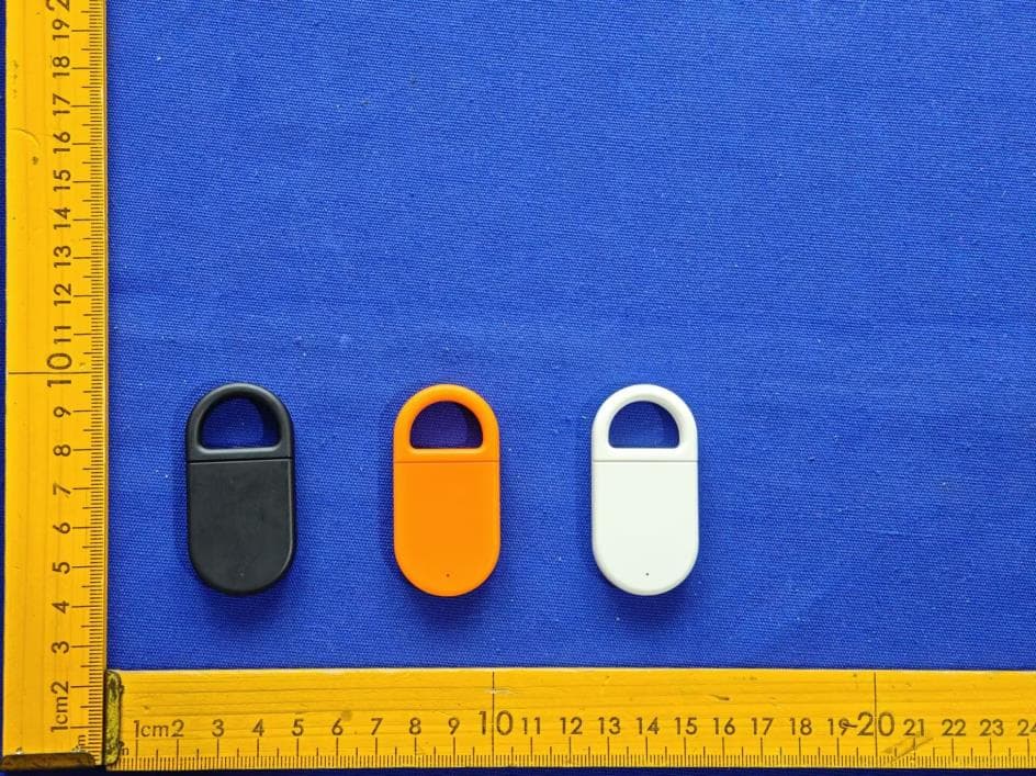
2BAUM-M21
Jul 27, 2026MOYAGOA Locator
Equipment Class
DTS - Digital Transmission System
2BAUM-M20
Jul 23, 2026ZERKAR Locator Tag
Equipment Class
DTS - Digital Transmission System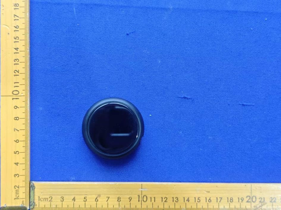
2BAUM-HZ02
Jun 05, 2026ZERKAR Badge
Equipment Class
DTS - Digital Transmission System
2BAUM-FM0007
Jan 06, 2026Find Locator Card
Equipment Class
DTS - Digital Transmission System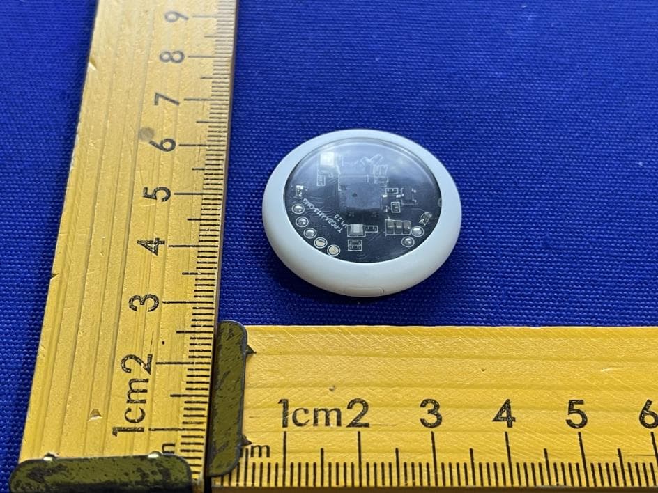
2BAUM-FM0006
Dec 08, 2025Locator Tag
Equipment Class
DTS - Digital Transmission System