2BBQT-INEB1446TWS EARBUDS
MCG Innovations Inc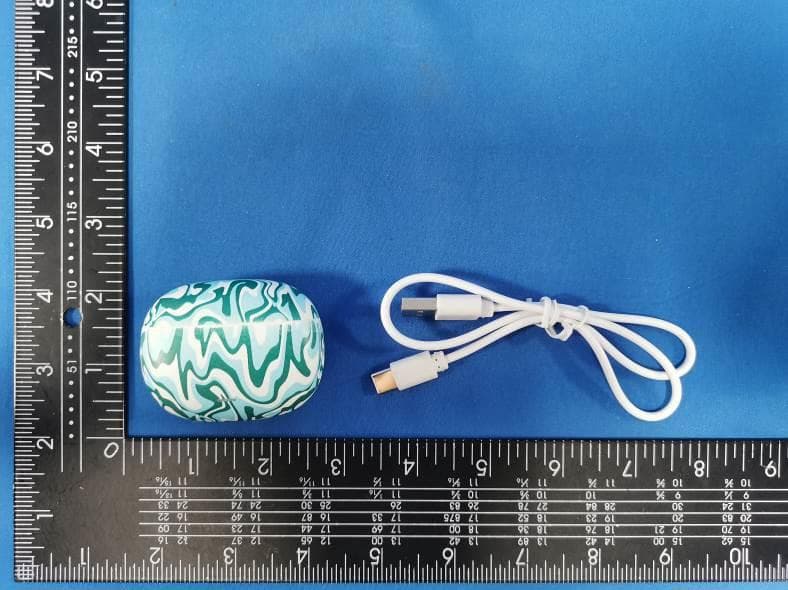
Click to zoom
Application Details
- Equipment Class
- DSS - Part 15 Spread Spectrum Transmitter
- Date of Grant
- Jul 04, 2023
- Application Purpose
- Original Equipment
- Date of Application
- Jul 04, 2023
- Equipment Note
- TWS EARBUDS
- Frequency Range
- 2402.00000000 - 2480.00000000
- Company
- MCG Innovations Inc
- Country
- United States
Documents & Files
Document Text
Text extracted from the exhibit documents filed with the FCC. Open a document above to read the original.
Users Manual
What's in the Box? 1 pair of earbuds 1 charging case (M size installed on earbuds) USB-C® charging cable 1 quick start guide 1 warranty card Step 1: Place your earbuds into the charging case for included charging cable. Step 2: Once fully charged, open the charging case. named "" and tap to connect. Removing your earbuds from the charging case will connect them to the last paired device. Placing your earbuds in the charging case and closing the last paired device. charging case by pressing and holding each side of the earbuds for 5 seconds. To unpair your earbuds from the previously connected earbuds in the charging case with the lid open to pair to a new device. S L INEB1446GR Ω 169
Attestation Statements
MCG Innovations Inc 246 Monmouth Rd. Oakhurst New Jersey United States Federal Communications Commission Authorization and Evaluation Division Equipment Authorization Branch 7435 Oakland Mills Road Columbia, MD 21046 2023-7-5 U.S. Agent Designation MCG Innovations Inc acknowledges their consent for the following contact located in the United States to act as their agent for service of process for the equipment for which authorization is sought (FCC ID: 2BBQT-INEB1446): Name and company of U.S. agent: MCG Innovations Inc Physical U.S. address of agent: 246 Monmouth Rd. Oakhurst New Jersey United States FRN of U.S. agent: 0033904673 Email address of U.S. agent: [email protected] MCG Innovations Inc acknowledges their obligation to accept service of process on behalf of MCG Innovations Inc . MCG Innovations Inc with the FRN [0033904673] accepts its obligation to maintain an agent for service of process in the United States for no less than one year after either the grantee has permanently terminated all marketing and importation of the applicable equipment within the U.S., or the conclusion of any Commission-related administrative or judicial proceeding involving the equipment, whichever is later. By signing this form, we confirm the above and that we are aware of the application requirements listed under § 2.911(d)(7). The information provided in this letter is based on the referenced rule parts of Title 47 of the CFR as well as KDB 986446 D01. An expiration date for this letter does not exist. In case the U.S. agent changes, the grantee is obligated to notify the FCC within 30 days via the granting TCB. Sincerely, Signature Bao Qier Manager MCG Innovations Inc Signature Bao Qier Manager MCG Innovations Inc 48_[mo del] US_Agent_2.911(d)(7) - U, V0 5
Cover Letter(s)
Sincerely, Name/Title: Bao Qier /Manager Company: MCG Innovations Inc Address: 246 Monmouth Rd. Oakhurst New Jersey United States Phone: 15920020358 Fax: N/A E-Mail: [email protected]
External Photos
FCC ID: 2BBQT-INEB1446 External Photos of the EUT Photo 1 Photo 2 Photo 3 FCC ID: 2BBQT-INEB1446 Left side Photo 4 Photo 5 Photo 6 FCC ID: 2BBQT-INEB1446 Photo 7 Photo 8 Photo 9 FCC ID: 2BBQT-INEB1446 Photo 10 Right side Photo 11 Photo 12 FCC ID: 2BBQT-INEB1446 Photo 13 Photo 14 Photo 15 FCC ID: 2BBQT-INEB1446 Photo 16 Photo 17
ID Label/Location Info
Label and Location Size: L: 1.0cm*W: 0.5cm Label and Location FCC ID : 2BBQT-INEB1446
Internal Photos
FCC ID: 2BBQT-INEB1446 Internal Photos of the EUT Left side Photo 1 Photo 2 Photo 3 FCC ID: 2BBQT-INEB1446 Photo 4 Photo 5 Photo 6 BT Chip Antenna FCC ID: 2BBQT-INEB1446 Photo 7 Photo 8 Photo 9 FCC ID: 2BBQT-INEB1446 Right side Photo 10 Photo 11 Photo 12 FCC ID: 2BBQT-INEB1446 Photo 13 Photo 14 Photo 15 BT Chip Antenna FCC ID: 2BBQT-INEB1446 Photo 16 Photo 17 Photo 18
RF Exposure Info
RF Exposure evaluation FCC ID: 2BBQT-INEB1446 1.1. Applicable Standard According to §1.1307(b)(1), systems operating under the provisions of this section shall be operated in a manner that ensures that the public is not exposed to radio frequency energy level in excess of the Commission’s guidelines. According to §1.1310 and §2.1093 RF exposure requirement KDB447498 v06: Mobile and Portable Devices RF Exposure Procedures and Equipment Authorization Policies 1.2. Requirement According to KDB447498 D01 General RF Exposure Guidance v06 Section 4.3.1 Standalone SAR test exclusion considerations: “Unless specifically required by the published RF exposure KDB procedures, standalone 1-g head or body and 10-g extremity SAR evaluation for general population exposure conditions, by measurement or numerical simulation, is not required when the corresponding SAR Test Exclusion Threshold condition, listed below, is satisfied. These test exclusion conditions are based on source-based time-averaged maximum conducted output power of the RF channel requiring evaluation, adjusted for tune-up tolerance, and the minimum test separation distance required for the exposure conditions.22 The minimum test separation distance is determined by the smallest distance from the antenna and radiating structures or outer surface of the device, according to the host form factor, exposure conditions and platform requirements, to any part of the body or extremity of a user or bystander (see 5) of section 4.1). To qualify for SAR test exclusion, the test separation distances applied must be fully explained and justified by the operating configurations and exposure conditions of the transmitter and applicable host platform requirements, typically in the SAR measurement or SAR analysis report, according to the required published RF exposure KDB procedures. When no other RF exposure testing or reporting is required, a statement of justification and compliance must be included in the equipment approval, in lieu of the SAR report, to qualify for the SAR test exclusion. When required, the device specific conditions described in the other published RF exposure KDB procedures must be satisfied before applying these SAR test exclusion provisions; for example, handheld PTT two-way radios, handsets, laptops & tablets etc.23 “ [(max. power of channel, including tune-up tolerance, mW)/ (min. test separation distance, mm)] · [√f (GHz)] ≤ 3.0 for 1-g SAR and ≤ 7.5 for 10-g extremity SAR, where: • f (GHz) is the RF channel transmit frequency in GHz • Power and distance are rounded to the nearest mW and mm before calculation • The result is rounded to one decimal place for comparison • 3.0 and 7.5 are referred to as the numeric thresholds in the step 2 below The test exclusions are applicable only when the minimum test separation distance is ≤ 50 mm and for transmission frequencies between 100 MHz and 6 GHz. When the minimum test separation distance is < 5 mm, a distance of 5 mm according to 5) in section 4.1 is applied to determine SAR test exclusion. 1.3. Manufacturing tolerance GFSK (Peak) Channel Channel 0 Channel 39 Channel 78 Target (dBm) -2.0 -2.0 -2.0 Tolerance ±(dB) 1.0 1.0 1.0 π/4DQPSK (Peak) Channel Channel 0 Channel 39 Channel 78 Target (dBm) -1.0 0.0 0.0 Tolerance ±(dB) 1.0 1.0 1.0 Page 2 of 2 2. E v a l u a t i o n R e s u l t Evaluation Results Band/Mode f (GHz) Antenna Distance (mm) RF output power (including tune-up tolerance) SAR Test Exclusion Threshold SAR Test Exclusion dBm mW BT 2.450 5 1.0 1.2589 0.3941<3.0 Yes 3. C o n c l u s i o n The measurement results comply with the FCC Limit per 47 CFR 2.1093 for the uncontrolled RF Exposure and SAR Exclusion Threshold per KDB 447498 v06 .....................End of Report.........................
Test Report
2.4GHz2012ChipAntenna:RANT2012F245C07 Dimension(mm) L2.05+-0.15 W1.20+-0.15 T0.85+-0.10 No.TerminalName 1Feeding/GNG 2GND Application: WLAN,802.11b/g,Bluetooth,WLAN,etc... Features SMD,highreliability,ultraImpact,Omni-directional... PartnumberInformation RANT2012F245C07 (A)(B)(C)(D)(E)(F) (A)ProductTypeChipAntenna (B)SizeCode2.0x1.2mm(+-0.2mm) (C)MaterialHighKmaterial (D)Frequency2.4~2.5GHz (E)FeedingmodePIFA&SingleFeeding (F)AntennatypeType=06 ElectricalSpecification WorkingFrequencyRange2400~2484MHz Bandwidth84(Min.) PeakGain2.0dBi(Typ.) Impedance50Ohm Returnloss10dB(Min) PolarizationLinear AzimuthBeamwidthOmni-directional OperationTemperature( °C )-40~85 °C ResistancetoSolderingHeats 10sec.(@280°C) TerminationNi/Au(Leadless) ThespecificationisdefinedonEVB. DimensionandTerminalConfiguration RAINInternationalTechnologyCo.,Ltd.TEL:13530576606 2.4GHz2012ChipAntenna:RANT2012F245C07 EvaluationBoardReference PCBDimensionAntennaLayoutReference Unit:mm ElectricalCharacteristics ReturnLoss ReturnLoss&Radiation 1 Frequency(MHz) S11(dB) 2400-10.77 2450-24.81 2484-10.243 Radiation Z Y X 2400MHz2450MHz2500MHz Efficiency70.56%75.25%71.01% PeakGain1.72dBi1.95dBi1.69dBi Directivity2.26dBi2.69dBi2.11dBi 2.4GHz2012ChipAntenna:RANT2012F245C07 TapingSpecifications ReelandTapingSpecification ReelSpecification TYPESIZEABCD 20127”5K/Reel 9.0±0.5 60±213.5±0.5178±2 TappingSpecification PackagingTypeABWEFGHTDP PaperType2012 1.50±0.202.30±0.208.0±0.201.75±0.103.5±0.054.0±0.102.0±0.050.75±0.101.57±0.104.0±0.1 2.4GHz2012ChipAntenna:RANT2012F245C07 ReliabilityTable TestItemProcedure Requirements CeramicType Remark (Reference) Electrical Characterization Fulfilltheelectrical specification UserSpec. Thermal Shock 1.Preconditioning: 50±10°C/1hr,thenkeepfor24±1hrsatroomtemp. 2.Initialmeasure:Spec:referInitialspec. 3.Rapidchangeoftemperaturetest: -30°Cto+85°C;100cycles; 15minutesatLowercategorytemperature; 15minutesatUppercategorytemperature. NoVisibleDamage. Fulfilltheelectrical specification. MIL-STD-202 107 Temperature Cycling 1.Initialmeasure:Spec:referInitialspec. 2.100Cycles(-30°Cto+85°C),SoakMode=1(2Cycle/hours). 3.Measurementat24±2Hoursaftertestcondition. NoVisibleDamage. Fulfilltheelectrical specification. JESD22 JA104 HighTemperature Exposure 1.Initialmeasure:Spec:referInitialspec. 2.Unpowered;500hours@T=+85°C. 3.Measurementat24±2hoursaftertest. NoVisibleDamage. Fulfilltheelectrical specification. MIL-STD-202 108 LowTemperature Storage 1.Initialmeasure:Spec:referInitialspec. 2.Unpowered:500hours@T=-30°C. 3.Measurementat24±2hoursaftertest. NoVisibleDamage. Fulfilltheelectrical specification. MIL-STD-202 108 Solderability (SMDBottomSide) Dippingmethod: a.Temperature:235±5°C b.Dippingtime:3±0.5s Thesoldershouldcover over95%ofthecritical areaofbottomside. IEC60384-21/22 4.10 SolderingHeat Resistance (RSH) Preheatingtemperature:150±10°C. Preheatingtime:1~2min. Soldertemperature:260±5°C. Dippingtime:5±0.5s NoVisibleDamage.IEC60384-21/22 4.10 Vibration5g'sfor20min.,12cycleseachof3orientations Note:Use8"X5"PCB.031"thick7securepointson,onelong sideand2securepointsatcornersofoppositesides.Parts mountedwithin2"fromanysecurepoint.Testfrom10-2000 Hz. NoVisibleDamage.MIL-STD-202 Method204 Mechanical Shock Threeshocksineachdirectionshallbeappliedalongthethree mutuallyperpendicularaxesofthetestspecimen(18shocks) Peakvalue:1,500g’s Duration:0.5ms Velocitychange:15.4ft/s Waveform:Half-sine NoVisibleDamage.MIL-STD-202 Method213 Humidity Bias 1.Humidity:85%R.H.,Temperature:85±2°C. 2.Time:500±24hours. 3.Measurementat24±2hrsaftertestcondition. NoVisibleDamage. Fulfilltheelectrical specification. MIL-STD-202 Method106 2.4GHz2012ChipAntenna:RANT2012F245C06 2.4GHz2012ChipAntenna:RANT2012F245C07 _ Board Flex (SMD) 1.Mountingmethod: IR-Reflow.PCBSize(L:100×W:40×T:1.6mm) 2.Applytheloadindirectionofthearrowuntilbendingreaches 2mm. NoVisibleDamage.AEC-Q200 005 AdhesionForceof1.8Kgfor60seconds.NoVisibleDamage Magnificationof20Xor greatermaybeemployed forinspectionofthe mechanicalintegrityofthe devicebodyterminalsand body/terminaljunction. AEC-Q200 006 Physical Dimension Anyapplicablemethodusingx10magnification,micrometers, calipers,gauges,contourprojectors,orothermeasuring equipment,capableofdeterminingtheactualspecimen dimensions. Inaccordancewith specification. JESD22 JB100 RevisionHistory RevisionDateContent 12020/10/15NewDatasheet
Test Report
Shenzhen CTA Testing Technology Co., Ltd. Room 106, Building 1, Yibaolai Industrial Park, Qiaotou Community, Fuhai Street, Bao’an District, Shenzhen, China Shenzhen CTA Testing Technology Co., Ltd. Room 106, Building 1, Yibaolai Industrial Park, Qiaotou Community, Fuhai Street, Bao’an District, Shenzhen, China Tel:+86-755 2322 5875 E-mail:[email protected] Web:http://www.cta-test.cn FCC PART 15 SUBPART C TEST REPORT FCC PART 15.247 Report Reference No. ..................... : FCC ID. ........................................... : CTA23062001401 2BBQT-INEB1446 Compiled by ( position+printed name+signature) .. : File administrators Zoey Cao Supervised by ( position+printed name+signature) .. : Project Engineer Amy Wen Approved by ( position+printed name+signature) .. : RF Manager Eric Wang Date of issue ..................................... : Jun. 26, 2023 Testing Laboratory Name .............. : Shenzhen CTA Testing Technology Co., Ltd. Address ............................................ : Room 106, Building 1, Yibaolai Industrial Park, Qiaotou Community, Fuhai Street, Bao‘an District, Shenzhen, China Applicant’s name ............................ : MCG Innovations Inc Address ............................................ : 246 Monmouth Rd. Oakhurst, NJ 07755 Test specification ...........................: Standard ........................................... : FCC Part 15.247 Shenzhen CTA Testing Technology Co., Ltd. All rights reserved. This publication may be reproduced in whole or in part for non-commercial purposes as long as the Shenzhen CTA Testing Technology Co., Ltd. is acknowledged as copyright owner and source of the material. Shenzhen CTA Testing Technology Co., Ltd. takes no responsibility for and will not assume liability for damages resulting from the reader's interpretation of the reproduced material due to its placement and context. Test item description ..................... : TWS EARBUDS Trade Mark ....................................... : N/A Manufacturer .................................... : Ningbo Haishu Wade Crafts Co., Ltd Model/Type reference....................... : INEB1446 Listed Models .................................. : INEB1446GR,INEB1446PP,BIEB1672,BIEB1673,IVEB1674, IVEB1675,IVEB1676,IVEB1677,IVEB1678,IVEB1679,IVEB1680, IVEB1681 Modulation ....................................... : GFSK, Π/4DQPSK Frequency .......................................... From 2402MHz to 2480MHz Rating ............................................... : DC 3.7V From Battery and DC 5.0V From external circuit Result................................................ : PASS Report No.: CTA23062001401 Page 2 of 50 Shenzhen CTA Testing Technology Co., Ltd. Room 106, Building 1, Yibaolai Industrial Park, Qiaotou Community, Fuhai Street, Bao’an District, Shenzhen, China Tel:+86-755 2322 5875 E-mail:[email protected] Web:http://www.cta-test.cn T E S T R E P O R T Equipment under Test : TWS EARBUDS Model /Type : INEB1446 Listed Models : INEB1446GR,INEB1446PP,BIEB1672,BIEB1673,IVEB1674, IVEB1675,IVEB1676,IVEB1677,IVEB1678,IVEB1679,IVEB1680, IVEB1681 Applicant : MCG Innovations Inc Address : 246 Monmouth Rd. Oakhurst, NJ 07755 Manufacturer : Ningbo Haishu Wade Crafts Co., Ltd Address : No. 82-102 Gongmao 4th Road Jishigang Town, Ningbo, Zhejiang, China Test Result: PASS The test report merely corresponds to the test sample. It is not permitted to copy extracts of these test result without the written permission of the test laboratory. Report No.: CTA23062001401 Page 3 of 50 Shenzhen CTA Testing Technology Co., Ltd. Room 106, Building 1, Yibaolai Industrial Park, Qiaotou Community, Fuhai Street, Bao’an District, Shenzhen, China Tel:+86-755 2322 5875 E-mail:[email protected] Web:http://www.cta-test.cn Contents 1 T E S T S T A N D A R D S .................................................................. 4 2 S U M M A R Y ............................................................................. 5 2.1 General Remarks 5 2.2 Product Description 5 2.3 Equipment Under Test 5 2.4 Short description of the Equipment under Test (EUT) 5 2.5 EUT operation mode 6 2.6 Block Diagram of Test Setup 6 2.7 Related Submittal(s) / Grant (s) 6 2.8 Modifications 6 3 T E S T E N V I R O N M E N T ............................................................... 7 3.1 Address of the test laboratory 7 3.2 Test Facility 7 3.3 Environmental conditions 7 3.4 Summary of measurement results 8 3.5 Statement of the measurement uncertainty 8 3.6 Equipments Used during the Test 9 4 T E S T C O N D I T I O N S A N D R E S U L T S ............................................ 10 4.1 AC Power Conducted Emission 10 4.2 Radiated Emission 13 4.3 Maximum Peak Output Power 19 4.4 20dB Bandwidth 20 4.5 Frequency Separation 23 4.6 Number of hopping frequency 25 4.7 Time of Occupancy (Dwell Time) 27 4.8 Out-of-band Emissions 30 4.9 Antenna Requirement 37 5 T E S T S E T U P P H O T O S O F T H E E U T .......................................... 38 6 P H O T O S O F T H E E U T ............................................................. 39 Report No.: CTA23062001401 Page 4 of 50 Shenzhen CTA Testing Technology Co., Ltd. Room 106, Building 1, Yibaolai Industrial Park, Qiaotou Community, Fuhai Street, Bao’an District, Shenzhen, China Tel:+86-755 2322 5875 E-mail:[email protected] Web:http://www.cta-test.cn 1 T E S T S T A N D A R D S The tests were performed according to following standards: FCC Rules Part 15.247: Frequency Hopping, Direct Spread Spectrum and Hybrid Systems that are in operation within the bands of 902-928 MHz, 2400-2483.5 MHz, and 5725-5850 MHz. ANSI C63.10-2013: American National Standard for Testing Unlicensed Wireless Devices Report No.: CTA23062001401 Page 5 of 50 Shenzhen CTA Testing Technology Co., Ltd. Room 106, Building 1, Yibaolai Industrial Park, Qiaotou Community, Fuhai Street, Bao’an District, Shenzhen, China Tel:+86-755 2322 5875 E-mail:[email protected] Web:http://www.cta-test.cn 2 S U M M A R Y 2.1 General Remarks Date of …
Text truncated - open the document above for the full version.
Test Report
Report No.: CTA23062001401 Page 34 of 50 Shenzhen CTA Testing Technology Co., Ltd. Room 106, Building 1, Yibaolai Industrial Park, Qiaotou Community, Fuhai Street, Bao’an District, Shenzhen, China Tel:+86-755 2322 5875 E-mail:[email protected] Web:http://www.cta-test.cn Band-edge Measurements for RF Conducted Emissions: GFSK Left Band edge hoping off Right Band edge hoping off Left Band edge hoping on Right Band edge hoping on Report No.: CTA23062001401 Page 35 of 50 Shenzhen CTA Testing Technology Co., Ltd. Room 106, Building 1, Yibaolai Industrial Park, Qiaotou Community, Fuhai Street, Bao’an District, Shenzhen, China Tel:+86-755 2322 5875 E-mail:[email protected] Web:http://www.cta-test.cn π/4DQPSK Left Band edge hoping off Right Band edge hoping off Left Band edge hoping on Right Band edge hoping on Report No.: CTA23062001401 Page 36 of 50 Shenzhen CTA Testing Technology Co., Ltd. Room 106, Building 1, Yibaolai Industrial Park, Qiaotou Community, Fuhai Street, Bao’an District, Shenzhen, China Tel:+86-755 2322 5875 E-mail:[email protected] Web:http://www.cta-test.cn Pseudorandom Frequency Hopping Sequence TEST APPLICABLE For 47 CFR Part 15C section 15.247 (a) (1) requirement: Frequency hopping systems shall have hopping channel carrier frequencies separated by a minimum of 25 kHz or the 20 dB bandwidth of the hop-ping channel, whichever is greater. Alternatively, frequency hopping systems operating in the 2400–2483.5 MHz band may have hopping channel carrier frequencies that are separated by 25 kHz or two-thirds of the 20 dB bandwidth of the hopping channel, whichever is greater, provided the systems operate with an output power no greater than 125 mW. The system shall hop to channel frequencies that are selected at the system hopping rate from a pseudo randomly ordered list of hopping frequencies. Each frequency must be used equally on the average by each transmitter. The system receivers shall have input bandwidths that match the hop-ping channel bandwidths of their corresponding transmitters and shall shift frequencies in synchronization with the transmitted signals. EUT Pseudorandom Frequency Hopping Sequence Requirement The pseudorandom frequency hopping sequence may be generated in a nice-stage shift register whose 5 th and 9 th stage outputs are added in a modulo-two addition stage. And the result is fed back to the input of the first stage. The sequence begins with the first one of 9 consecutive ones, for example: the shift register is initialized with nine ones. ● Number of shift register stages:9 ● Length of pseudo-random sequence:29-1=511 bits ● Longest sequence of zeros:8(non-inverted signal) An example of pseudorandom frequency hopping sequence as follows: Each frequency used equally one the average by each transmitter. The system receiver have input bandwidths that match the hopping channel bandwidths of their corresponding transmitter and shift frequencies in synchronization with the transmitted signals. Report No.: CTA23062001401 Page 37 of 50 Shenzhen CTA Testing Technology Co., Ltd. Room 106, Building 1, Yibaolai Industrial Park, Qiaotou Community, Fuhai Street, Bao’an District, Shenzhen, China Tel:+86-755 2322 5875 E-mail:[email protected] Web:http://www.cta-test.cn 4.9 Antenna Requirement Standard Applicable For intentional device, according to FCC 47 CFR Section 15.203, an intentional radiator shall be designed to ensure that no antenna other than that furnished by the responsible party shall be used with the device. And according to FCC 47 CFR Section 15.247 (c), if transmitting antennas of directional gain greater than 6dBi are used, the power shall be reduced by the amount in dB that the directional gain of the antenna exceeds 6dBi. Refer to statement below for compliance The manufacturer may design the unit so that the user can replace a broken antenna, but the use of a standard antenna jack or electrical connector is prohibited. Further, this requirement does not apply to intentional radiators that must be professionally installed. Antenna Connected Construction The maximum gain of antenna was 2.00 dBi. Remark:The antenna gain is provided by the customer , if the data provided by the customer is not accurate, Shenzhen CTA Testing Technology Co., Ltd. does not assume any responsibility. Report No.: CTA23062001401 Page 38 of 50 Shenzhen CTA Testing Technology Co., Ltd. Room 106, Building 1, Yibaolai Industrial Park, Qiaotou Community, Fuhai Street, Bao’an District, Shenzhen, China Tel:+86-755 2322 5875 E-mail:[email protected] Web:http://www.cta-test.cn 5 T e s t S e t u p P h o t o s o f t h e E U T Report No.: CTA23062001401 Page 39 of 50 Shenzhen CTA Testing Technology Co., Ltd. Room 106, Building 1, Yibaolai Industrial Park, Qiaotou Community, Fuhai Street, Bao’an District, Shenzhen, China Tel:+86-755 2322 5875 E-mail:[email protected] Web:http://www.cta-test.cn 6 P h o t o s o f t h e E U T Report No.: CTA23062001401 Page 40 of 50 Shenzhen CTA Testing Technology Co., Ltd. Room 106, Building 1, Yibaolai Industrial Park, Qiaotou Community, Fuhai Street, Bao’an District, Shenzhen, China Tel:+86-755 2322 5875 E-mail:[email protected] Web:http://www.cta-test.cn Left side Report No.: CTA23062001401 Page 41 of 50 Shenzhen CTA Testing Technology Co., Ltd. Room 106, Building 1, Yibaolai Industrial Park, Qiaotou Community, Fuhai Street, Bao’an District, Shenzhen, China Tel:+86-755 2322 5875 E-mail:[email protected] Web:http://www.cta-test.cn Report No.: CTA23062001401 Page 42 of 50 Shenzhen CTA Testing Technology Co., Ltd. Room 106, Building 1, Yibaolai Industrial Park, Qiaotou Community, Fuhai Street, Bao’an District, Shenzhen, China Tel:+86-755 2322 5875 E-mail:[email protected] Web:http://www.cta-test.cn Report No.: CTA23062001401 Page 43 of 50 Shenzhen CTA Testing Technology Co., Ltd. Room 106, Building 1, Yibaolai Industrial Park, Qiaotou Community, Fuhai Street, Bao’an District, Shenzhen, China Tel:+86-755 2322 5875 E-mail:[email protected] Web:http://www.cta-test.cn Report No.: …
Text truncated - open the document above for the full version.
Test Setup Photos
FCC ID: 2BBQT-INEB1446 Test Setup Photos of the EUT
Contact Information
Applicant
Bao Qier
Test Firm
SHENZHEN CTA TESTING TECHNOLOGY CO., LTD.Eric Wang
[email protected]+86 755 2322 5875
Technical Specifications
| # | Rule Parts | Frequency Range | Power Output |
|---|---|---|---|
| 1 | 15C | 2.40 GHz - 2.48 GHz | 900.00 µW |
Other Applications from MCG Innovations Inc
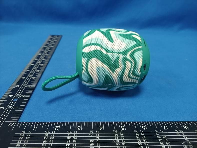
2BBQT-INSP1448
Aug 05, 2023SPEAKER
Equipment Class
DSS - Part 15 Spread Spectrum Transmitter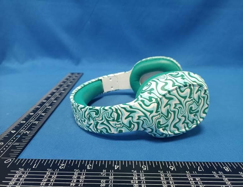
2BBQT-INHP1447
Jul 04, 2023HEADPHONE
Equipment Class
DSS - Part 15 Spread Spectrum Transmitter