FCCID.CO- FCC ID Database
HomeCompaniesEquipment ClassesSearch

© 2026 FCC ID Database. All rights reserved.

AboutContactData sourced from FCC public records
  1. Home/
  2. Guangdong Sanenshi Intelligent Technology Co., Ltd./
  3. 2BCI9-TS8500

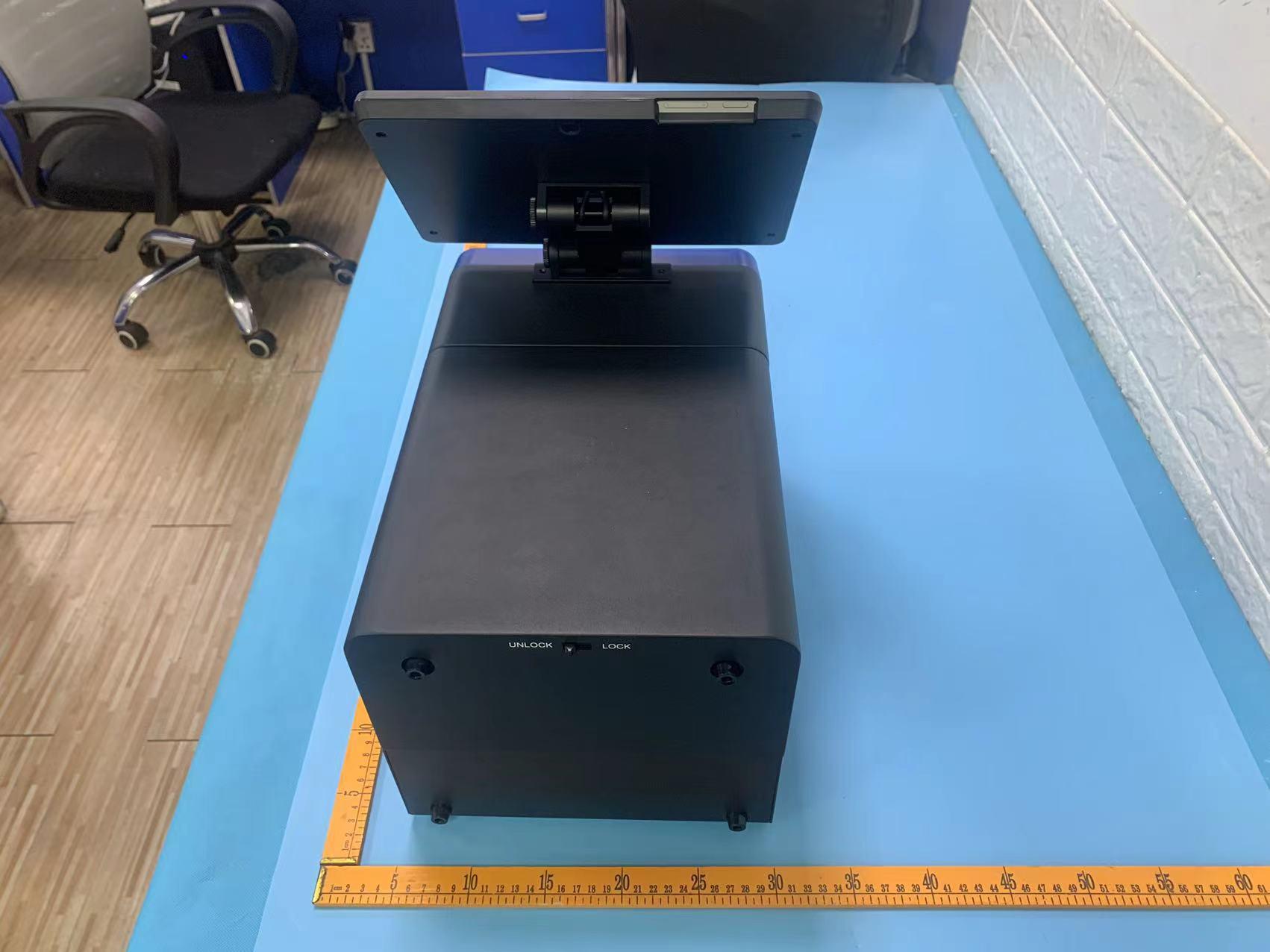
2BCI9-TS8500Benchtop Spectrophotometers

Guangdong Sanenshi Intelligent Technology Co., Ltd.
Benchtop Spectrophotometers - FCC ID 2BCI9-TS8500 - Guangdong Sanenshi Intelligent Technology Co., Ltd.
Click to zoom

Application Details

Equipment Class
DTS - Digital Transmission System
Date of Grant
Sep 13, 2023
Application Purpose
Original Equipment
Date of Application
Sep 13, 2023
Equipment Note
Benchtop Spectrophotometers
Frequency Range
2402.00000000 - 2480.00000000
Company
Guangdong Sanenshi Intelligent Technology Co., Ltd.
Country
China

Documents & Files

Select a file to view
Users Manual

↗

Attestation Statements

↗
↗

Cover Letter(s)

↗
↗
↗

External Photos

↗

ID Label/Location Info

↗

Internal Photos

↗

RF Exposure Info

↗

Test Report

↗
↗

Test Setup Photos

↗

Document Text

Text extracted from the exhibit documents filed with the FCC. Open a document above to read the original.

Users Manual

Bluetooth 5G UWB PM 5:16 Color search PT_Solid_Coated_D8 SCI / D65 / 10° #FA75B3 Result: PT_Sol_Coated 211 C 5U SCE L*=67.72 a*=55.11 b*=-8.71 PT_Sol_Coated 236 C 5U Color search Bluetooth 5G UWB PM 5:16 2021-08-2417:16:38T14S89 Type Standard Sample L*a*b* 81.55-74.3865.01 52.899.6954.44 SCI/D65/10°/Φ4mm CIEDE(△E*ab)=38.13 Measure Bluetooth 5G UWB PM 5:16 2021-08-2417:16:38T14S89 Type Standard Sample L*a*b* 81.55-74.3865.01 52.899.6954.44 SCI/D65/10°/Φ4mm CIEDE(△E*ab)=38.13 Measure

Attestation Statements

GuangdongSanenshiIntelligentTechnologyCo.,Ltd. CoveredEquipmentCertificationAttestationLetter DATE FederalCommunicationsCommission AuthorizationandEvaluationDivision 7435OaklandMillsRoad Columbia,MD21046 USA ATTN.:ReviewingEngineer FCCID:2BCI9-TS8500 GuangdongSanenshiIntelligentTechnologyCo.,Ltd.(“theapplicant”)certifiesthatthe equipmentforwhichauthorizationissoughtisnot“covered”equipmentprohibitedfrom receivinganequipmentauthorizationpursuanttosection2.903oftheFCCrules. Note:Iftheequipmentforwhichtheapplicantseeksauthorizationisproducedby anyoftheentitiesidentifiedonthecurrentCoveredList,theapplicantshould includeanexplanationonwhytheequipmentisnot“covered”equipment. GuangdongSanenshiIntelligentTechnologyCo.,Ltd.(“theapplicant”)certifiesthat,asof thedateofthefilingoftheapplication,theapplicantisnotidentifiedontheCoveredList asanentityproducing“covered”equipment. Signed: Printedname:ZhiyongHuang Title:manager CompanyName:GuangdongSanenshiIntelligentTechnologyCo.,Ltd. Date:2023/9/11

Attestation Statements

GuangdongSanenshiIntelligentTechnologyCo., Ltd. * theapplicantmustdesignateacontactlocatedintheUnitedStatesforpurposesofactingasthe applicant’sagentforserviceofprocess,regardlessofwhethertheapplicantisadomesticorforeign entity.AnapplicantlocatedintheUnitedStatesmaydesignateitselfastheagentforserviceofprocess. U.S.AgentDesignationforServiceofProcess- CertificationAttestationLetter DATE TO:FederalCommunicationsCommission 7435OaklandMillsRoad Columbia,MD21046 ApplicantSigned ATTN.: Reviewing Engineer FCC ID: 2BCI9-TS8500 FRN of applicant: 0034135319 Per section 2.911(d)(7) of the FCC rules,Guangdong Sanenshi Intelligent Technology Co., Ltd. (“the applicant”) certifies that the equipment for which authorization is sought is designated to the following U.S. agent* for service of process: Company Name: Stone Trading Limited FCC Registration Number (FRN): 0033401936 Physical U.S. Company Address: 6547 N Academy Blvd #2266,Colorado Springs,CO 80918,United States Contact Person: Dongmei Fang Agent Email Address: [email protected] The above contact person accepts the obligation for service of process. The applicant accepts to maintain an agent for no less than one year after the grantee has terminated all marketing and importation or the conclusion of any Commission-related proceeding involving the equipment. : Signed: Printedname: ZhiyongHuang Title:Manager CompanyName:GuangdongSanenshi IntelligentTechnologyCo.,Ltd. Date:2023/9/13 AgentSigned(ifdifferentfromApplicant): Signed: Printedname:DongmeiFang Title:Manager CompanyName:StoneTradingLimit Date:2023/9/13

Cover Letter(s)

DATE:2023/9/11 FederalCommunicationsCommission Authorization&EvaluationDivision 7345OaklandMillsRoad Columbia,Maryland21046 AuthoritytoActasAgent Onourbehalf,IappointShenzhenPOCETechnologyCo.,Ltd.Address:102BuildingH1 &1/F.,BuildingH,HongfaScience&TechnologyPark,Tangtou,Shiyan,Bao’anDistrict, Shenzhen,Guangdong,Chinatoactasouragentinthepreparationofthisapplicationfor equipmentcertification.Icertifythatsubmitteddocumentsproperlydescribethedeviceor systemforwhichequipmentcertificationissought.Ialsocertifythateachunit manufactured,importedormarketed,asdefinedintheFederalCommunications Commission’sregulationswillhaveaffixedtoitalabelidenticaltothatsubmittedfor approvalwiththisapplication. Forinstanceswhereourauthorizedagentsignstheapplicationforcertificationonour behalf,Iacknowledgethatallresponsibilityforcomplyingwiththetermsandconditionsfor certification,stillresideswithGuangdongSanenshiIntelligentTechnologyCo.,Ltd. Address:6-8/F,BuildingB33,Low-CarbonHeadquartersPark,400Xincheng Avenue,ZengchengDistrict,Guangzhou,P.R.China.(ApplicantNameandaddress) <Signature> Name:ZhiyongHuang Title:manager Company:GuangdongSanenshiIntelligentTechnologyCo.,Ltd.

Cover Letter(s)

DATE:2023/9/11 EquipmentAutorisationDivision FederalCommunicationsCommission 7435OaklandMillsRoad Columbia,MD21046 FCCID:2BCI9-TS8500 ProductName:BenchtopSpectrophotometers RequestforConfidentiality PursuanttoSections0.457and0.459ofthecommission’srules,weherebyrequestthat thefollowingdocumentsbeheldconfidential: (Listherethedocumentsforwhichyouareseekingconfidentiality–forexample...)  Schematics Blockdiagram Operationdescription Thesematerialscontaintradesecretsandproprietaryinformationandarenot customarilyreleasedtothepublic.Thepublicdisclosureofthisinformationmightbe harmfultothecompanyandprovideunjustifiedbenefitstoourcompetitors. <Signature> Name:ZhiyongHuang Title:manager Company:GuangdongSanenshiIntelligentTechnologyCo.,Ltd.

Cover Letter(s)

FCC ID:2BCI9-TS8500 Guangdong Sanenshi Intelligent Technology Co., Ltd. Mo del Co nfirmation Letter We,Guangdong Sanenshi Intelligent Technology Co., Ltd., certify the product: Be nchtop Spe ctrophotometers, Model No.:TS8500,TS8500S , TS8510 , TS8520 , TS8560. The product has many models, only the model name is different, and the other parts such as the circuit principle, pcb and electrical structure are the same. Signiture: Zhiyong Huang Grantee Contact: +86-18207556812 Company Name: Guangdong Sane nshi Intelligent Te chnology Co., Ltd. Date: 2023/09/04

External Photos

FCCID:2BCI9-TS8500 External FCCID:2BCI9-TS8500 FCCID:2BCI9-TS8500 FCCID:2BCI9-TS8500 FCCID:2BCI9-TS8500 FCCID:2BCI9-TS8500

ID Label/Location Info

Label:50*30mm ProductName:BenchtopSpectrophotometers Model/Typereference:TS8500 FCCID:2BCI9-TS8500 GuangdongSanenshiIntelligentTechnologyCo.,Ltd.

Internal Photos

FCCID:2BCI9-TS8500 Internal ant FCCID:2BCI9-TS8500 FCCID:2BCI9-TS8500 FCCID:2BCI9-TS8500 FCCID:2BCI9-TS8500 FCCID:2BCI9-TS8500 FCCID:2BCI9-TS8500 FCCID:2BCI9-TS8500 FCCID:2BCI9-TS8500 FCCID:2BCI9-TS8500 FCCID:2BCI9-TS8500

RF Exposure Info

FCCID:2BCI9-TS8500 RFExposureEvaluation AccordingtoKDB447498D01GeneralRFExposureGuidancev064.3.1.StandaloneSARtest exclusionconsiderationsUnlessspecificallyrequiredbythepublishedRFexposureKDBprocedures, standalone1-gheadorbodyand10-gextremitySARevaluationforgeneralpopulationexposure conditions,bymeasurementornumericalsimulation,isnotrequiredwhenthecorrespondingSAR ExclusionThresholdcondition,listedbelow,issatisfied. Limits AccordingtoFCCPart1.1310:Thecriterialistedinthefollowingtableshallbeusedtoevaluatethe environmentimpactofhumanexposuretoradiofrequency(RF)radiationasspecifiedinpart1.1307(b) F=FrequencyinMHzFriisFormula Friistransmissionformula:Pd=(Pout*G)/(4*Pi*R2)Where Pd=powerdensityinmW/cm2 Pout=outputpowertoantennainmW G=gainofantennainlinearscale Pi=3.1416 R=distancebetweenobservationpointandcenteroftheradiatorincm PdidthelimitofMPE.Ifweknowthemaximumgainoftheantennaandthetotalpowerinputtotheantenna, throughthecalculation,wewillknowthedistancerwheretheMPElimitisreached. TestResultofRFExposureEvaluation Antennagain:1.34dBi AntennaGain:ThemaximumGainmeasuredinfullyanechoicchamberis1.0inlinearscale. OutputPowerIntoAntenna&RFExposureEvaluationDistance:20cm MeasurementData TheMaxConductedPeakOutputPowerdatarefertoreportReportNo.:POCE230803052BRW 1.1 EUT RF EXPOSURE OperationalMode:BLE(GFSKworstcase) Channel Maximum Peak Conducted OutputPower (dBm) Tuneup tolerance (dB) Maximumtune-upPower Calculated value (mW/cm2) Exclusion threshold (mW/cm2) (dBm)(mW) 2402MHZ-1.56 -1.56±1 -0.560.8790.0002381.0 Conclusion:the calculatedvalue≤1.0, SARis exempted. 1) Pd = (Pout*G)/(4* Pi * R2)=( 0.879 *1.361)/(4*3.14159*20*20)=0.000238 , G=10gain/10 = 1.361

Test Report

承認書 SPECIFICATION FOR APPROVAL 客戶名稱 CUSTOMER : 客戶料號 CUSTOMER’S P/N : 料號 PART NUMBER : WAN3216F245W36 規格 DESCRIPTION : Antenna 3216 M-Ant 2.45G Type 36 版本 VERSION : V2.2 日期 ISSUE DATE : 2018/01/30 客 戶 承 認 CUSTOMER APPROVED 工 程 部 R&D CENTER 承 認 APPROVAL 確 認 CHECKED 製 作 DRAWN Ray James Thor 萬誠科技股份有限公司 OneWave Electronic Co., Ltd. 112台北市北投區中央南路二段36號3樓 2F., No.163, Sec. 1, Xi'an St., Beitou Dist., Taipei City 112, Taiwan 電話: (02) 2898-2220 TEL: +886 2 2898-2220 傳真: (02) 2898-5055 FAX: +886 2 2898-5055 LUCKY SOUND TECHNOLOGY CO.,LTD ONEWAVE TECHNOLOGY CO., LTD. 2/11 For Bluetooth / WLAN A 3216 antenna pplications Dimension (mm) L 3.23 ± 0.20 W 1.66 ± 0.20 T 1.23 ± 0.20 P/N: WAN3216F245W36 ONEWAVE TECHNOLOGY CO., LTD. 3/11 Part Number Information WAN 3216 F 245 W 36 A B C D E F A Product Series Antenna B Dimension L x W 3.2X1.6mm (+-0.2mm) C Material High K material D Working Frequency 2.4 ~ 2.5GHz E Feeding mode Monopole & Single Feeding F Antenna type Type=36 1. Electrical Specification Remark : Bandwidth & Peak Gain was measured under evaluation board of next page Specification Part Number WAN3216F245W36 Central Frequency 2450 MHz Bandwidth 100 (Min.) MHz Return Loss -6.5 (Max) dB Peak Gain 1.34dBi Impedance 50 Ohm Operating Temperature -40~+85 °C Maximum Power 4 W Resistance to Soldering Heats 10 ( @ 260°C) sec. Polarization Linear Azimuth Beamwidth Omni-directional Termination Cu / Sn (Leadless) ONEWAVE TECHNOLOGY CO., LTD. 4/11 2. Recommended PCB Pattern 1.Evaluation Board Dimension 2.Evaluation Board Dimension (若淨空區夠大,建議使用此Layout,效能較佳) Unit : mm Suggested Matching Circuit 重要資訊 : 匹配元件建議使用精準度±1%以下的電感、電容、電阻 ONEWAVE TECHNOLOGY CO., LTD. 5/11 1.Layout Dimensions in Clearance area(Size=5.2*5.0mm) 50 ohm transmission Line Matching Circuit 2.Layout Dimensions in Clearance area(Size=8.2*5.0mm) (若淨空區夠大,建議使用此Layout,效能較佳) 50 ohm transmission Line Matching Circuit FootPrint (Unit : mm) ONEWAVE TECHNOLOGY CO., LTD. 6/11 3. Measurement Results Return Loss ONEWAVE TECHNOLOGY CO., LTD. 7/11 Radiation Pattern Efficiency Peak Gain Directivity 2400MHz 55.21 % 1.25 dBi5.32 dBi 2450MHz 66.45 % 1.34 dBi5.21 dBi 2500MHz 57.53 % 1.28 dBi5.29 dBi Chamber Coordinate System Y Z X ONEWAVE TECHNOLOGY CO., LTD. 8/11 4.Reliability and Test Condictions ITEM REQUIREMENTS TEST CONDITION Solderability 1. Wetting shall exceed 90% coverage 2. No visible mechanical damage Pre-heating temperature:150°C/60sec. Solder temperature:230±5°C Duration:4±1sec. Solder:Sn-Ag3.0-Cu0.5 Flux for lead free: rosin Solder heat Resistance 1. No visible mechanical damage 2. Central Freq. change :within ± 6% 10±0.5 sec. 60sec .. TEMP (°C) 150°C 260°C Pre-heating temperature:150°C/60sec. Solder temperature:260±5°C Duration:10±0.5sec. Solder:Sn-Ag3.0-Cu0.5 Flux for lead free: rosin Component Adhesion (Push test) 1. No visible mechanical damage The device should be reflow soldered(230±5°C for 10sec.) to a tinned copper substrate A dynometer force gauge should be applied the side of the component. The device must with-ST-F 0.5 Kg without failure of the termination attached to component. Component Adhesion (Pull test) 1. No visible mechanical damage Insert 10cm wire into the remaining open eye bend ,the ends of even wire lengths upward and wind together. Terminal shall not be remarkably damaged. Thermal shock 1. No visible mechanical damage 2. Central Freq. change :within ±6% Phase Temperature(°C) Time(min) 1 +85±5°C 30±3 2 Room Temperature Within 3sec 3 -40±2°C 30±3 4 Room Temperature Within 3sec +85°C=>30±3min -40°C=>30±3min Test cycle:10 cycles The chip shall be stabilized at normal condition for 2~3 hours before measuring. Resistance to High Temperature 1. No visible mechanical damage 2. Central Freq. change :within ±6% 3. No disconnection or short circuit. Temperature: 85±5°C Duration: 1000±12hrs The chip shall be stabilized at normal condition for 2~3 hours before measuring. Resistance to Low Temperature 1. No visible mechanical damage 2. Central Freq. change :within ±6% 3. No disconnection or short circuit. Temperature:-40±5°C Duration: 1000±12hrs The chip shall be stabilized at normal condition for 2~3 hours before measuring. Humidity 1. No visible mechanical damage 2. Central Freq. change :within ±6% 3. No disconnection or short circuit. Temperature: 40±2°C Humidity: 90% to 95% RH Duration: 1000±12hrs The chip shall be stabilized at normal condition for 2~3 hours before measuring. 4±1 sec. 60sec TEMP (°C) 150°C 230°C ONEWAVE TECHNOLOGY CO., LTD. 9/11 5.Soldering and Mounting Mildly activated rosin fluxes are preferred. The minimum amount of solder can lead to damage from the stresses caused by the difference in coefficients of expansion between solder, chip and substrate. The terminations are suitable for all wave and re-flow soldering systems. If hand soldering cannot be avoided, the preferred technique is the utilization of hot air soldering tools. Recommended temperature profiles for re-flow soldering in Figure 1. Products attachment with a soldering iron is discouraged due to the inherent process control limitations. In the event that a soldering iron must be employed the following precautions are recommended. ‧Preheat circuit and products to 150°C ‧Never contact the ceramic with the iron tip ‧Use a 20 watt soldering iron with tip diameter of 1.0mm ‧280°C tip temperature (max) ‧1.0mm tip diameter (max) ‧Limit soldering time to 3 sec. SOLDERING COOLING NATURAL PRE-HEATING TEMPERATURE(°C) 60~120 s 10s max. 30~60s 250~260 230 180 150 TIME(sec.) Reflow Soldering SOLDERING COOLING NATURAL PRE-HEATING TEMPERATURE(°C) within 3s Gradualcooling 150 TIME(sec.) Iron Soldering Over 60s 350 300 ONEWAVE TECHNOLOGY CO., LTD. 10/11 6.Packaging Information  Tape Specification: W Ao Bo Ko P F E D D1 Po P2 t 8.0 ±0.30 1.80 ±0.05 3.51 ±0.10 1.59 ±0.10 4.00 ±0.05 3.50 ±0.05 1.75 ±0.10 1.50 ±0.10 0.00 ±0.10 4.00 ±0.10 2.00 ±0.05 0.25 ±0.05  Reel Specification: (7’’, Φ180 mm) Tape Width(mm) A(mm) B(mm) C(mm) D(mm) Chip/Reel(pcs) 8 9.0±0.5 60±2 13.5±0.5 178±2…

Text truncated - open the document above for the full version.

Test Report

V1.0ReportNo.:POCE230803052BRW 102BuildingH1&1/F.,BuildingH,HongfaScience&TechnologyPark,Tangtou,Shiyan,Bao'anDistrict,Shenzhen,Guangdong,China Web:http://www.poce-cert.comTel:86-755-29113252E-mail:[email protected] 1 of 55 RFTESTREPORT For GuangdongSanenshiIntelligentTechnologyCo.,Ltd. ProductName:BenchtopSpectrophotometers Model(s).:TS8500 ReportReferenceNo.:POCE230803052BRW FCCID:2BCI9-TS8500 Applicant’sName:GuangdongSanenshiIntelligentTechnologyCo.,Ltd. Address: 6-8/F,BuildingB33,Low-CarbonHeadquartersPark,400Xincheng Avenue,ZengchengDistrict,Guangzhou,P.R.China. TestingLaboratory:ShenzhenPOCETechnologyCo.,Ltd. Address: 102BuildingH1&1/F.,BuildingH,HongfaScience&TechnologyPark, Tangtou,Shiyan,Bao’anDistrict,Shenzhen,Guangdong,China TestSpecificationStandard:47CFRPart15.247 DateofReceipt:August3,2023 DateofTest:August3,2023toAugust17,2023 DataofIssue:August17,2023 Result:Pass Note:Thisreportshallnotbereproducedexceptinfull,withoutthewrittenapprovalofShenzhenPOCE TechnologyCo.,Ltd.ThisdocumentmaybealteredorrevisedbyShenzhenPOCETechnologyCo.,Ltd. personnelonly,andshallbenotedintherevisionsectionofthedocument.Thetestresultsinthereportonly applytothetestedsample V1.0ReportNo.:POCE230803052BRW 102BuildingH1&1/F.,BuildingH,HongfaScience&TechnologyPark,Tangtou,Shiyan,Bao'anDistrict,Shenzhen,Guangdong,China Web:http://www.poce-cert.comTel:86-755-29113252E-mail:[email protected] 2 of 55 RevisionHistoryOfReport VersionDescriptionREPORTNo.IssueDate V1.0OriginalPOCE230803052BRWAugust17,2023 NOTE1: Themanufacturershouldensurethatallproductsinseriesproductionareinconformitywiththeproductsampledetailedin thisreport.Iftheproductinthisreportisusedinanyconfigurationotherthanthatdetailedinthereport,themanufacturer mustensurethenewsystemcomplieswithallrelevantstandards. Compiledby:Supervisedby:Approvedby: AmyZhu/FileadministratorsStoneYin/TechniqueprincipalMachaelMo/Manager V1.0ReportNo.:POCE230803052BRW 102BuildingH1&1/F.,BuildingH,HongfaScience&TechnologyPark,Tangtou,Shiyan,Bao'anDistrict,Shenzhen,Guangdong,China Web:http://www.poce-cert.comTel:86-755-29113252E-mail:[email protected] 3 of 55 CONTENTS 1TESTSUMMARY...................................................................................................................................................5 1.1TESTSTANDARDS........................................................................................................................................5 1.2SUMMARYOFTESTRESULT.........................................................................................................................5 2GENERALINFORMATION....................................................................................................................................6 2.1CLIENTINFORMATION..................................................................................................................................6 2.2DESCRIPTIONOFDEVICE(EUT)..................................................................................................................6 2.3DESCRIPTIONOFTESTMODES....................................................................................................................7 2.4DESCRIPTIONOFSUPPORTUNITS................................................................................................................7 2.5EQUIPMENTSUSEDDURINGTHETEST........................................................................................................7 2.6STATEMENTOFTHEMEASUREMENTUNCERTAINTY......................................................................................9 2.7IDENTIFICATIONOFTESTINGLABORATORY...................................................................................................9 2.8ANNOUNCEMENT.........................................................................................................................................9 3EVALUATIONRESULTS(EVALUATION)...........................................................................................................10 3.1ANTENNAREQUIREMENT............................................................................................................................10 3.1.1Conclusion:.................................................................................................................................10 4RADIOSPECTRUMMATTERTESTRESULTS(RF).........................................................................................11 4.1CONDUCTEDEMISSIONATACPOWERLINE................................................................................................11 4.1.1E.U.T.Operation:........................................................................................................................11 4.1.2TestSetupDiagram:...................................................................................................................11 4.1.3TestData:...................................................................................................................................12 4.2OCCUPIEDBANDWIDTH.............................................................................................................................14 4.2.1E.U.T.Operation:........................................................................................................................14 4.2.2TestSetupDiagram:...................................................................................................................14 4.2.3TestData:...................................................................................................................................14 4.3MAXIMUMCONDUCTEDOUTPUTPOWER....................................................................................................15 4.3.1E.U.T.Operation:........................................................................................................................15 4.3.2TestSetupDiagram:....................................................................................................…

Text truncated - open the document above for the full version.

Test Setup Photos

FCCID:2BCI9-TS8500 ConductedEmissionatACpowerline Emissionsinrestrictedfrequencybands(below1GHz) FCCID:2BCI9-TS8500 Emissionsinrestrictedfrequencybands(above1GHz)

Contact Information

Applicant

Zhiyong Huang
[email protected]+86-18207556812Fax: 86-755-29113135

Test Firm

Shenzhen DACE Testing Technology Co., Ltd.Colin Huang
[email protected]86 13267178997

Technical Specifications

#Rule PartsFrequency RangePower Output
115C2.40 GHz - 2.48 GHz698.70 µW
Confidentiality
Long Term
Grant Notes
Power output listed is conducted.

Other Applications from Guangdong Sanenshi Intelligent Technology Co., Ltd.

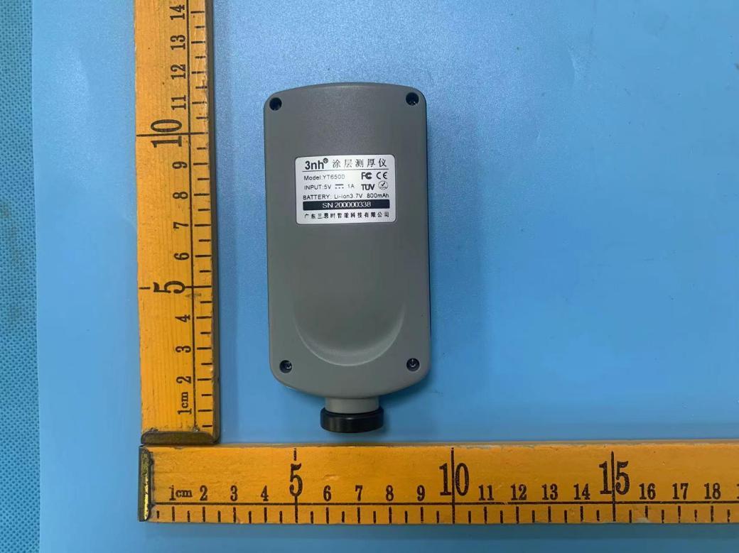
thickness gauge - FCC ID 2BCI9-YT6500 - Guangdong Sanenshi Intelligent Technology Co., Ltd.
2BCI9-YT6500

thickness gauge

Nov 19, 2023

Equipment Class

DTS - Digital Transmission System