2BG7T-TPL3937Bluetooth Module
Shanghai Tanpin Technology Co., Ltd.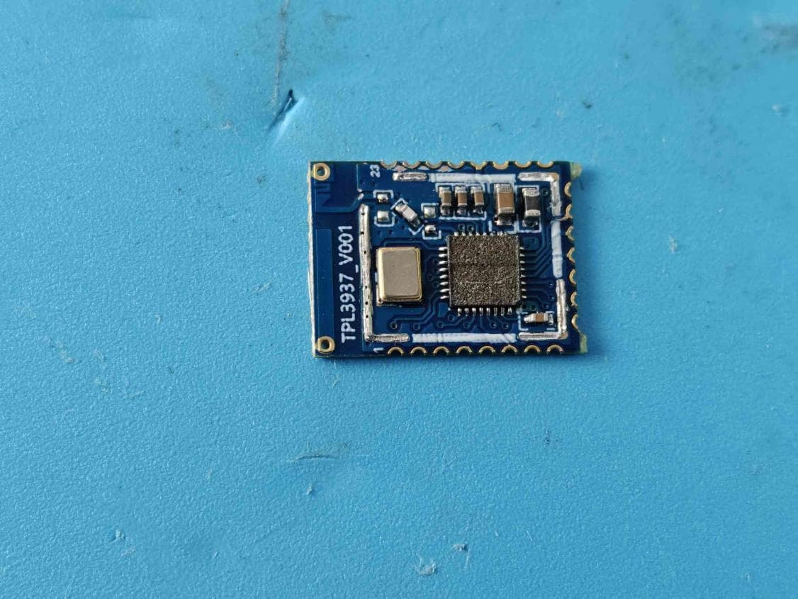
Click to zoom
Application Details
- Equipment Class
- DTS - Digital Transmission System
- Date of Grant
- Sep 03, 2024
- Application Purpose
- Original Equipment
- Date of Application
- Aug 25, 2024
- Equipment Note
- Bluetooth Module
- Frequency Range
- 2402.00000000 - 2480.00000000
- Country
- China
Documents & Files
Document Text
Text extracted from the exhibit documents filed with the FCC. Open a document above to read the original.
Users Manual
TPL3937 Dual Module Datasheet 版本:V1.0 版权:©2021 TPL3937 Dual Module Datasheet 一、Introduction 二、Module Parameters 三、Module Size 四、Pin Definition 五、Reference Design 六、Hardware Design Considerations 1、Module placement requirements on the bottom plate 2、power supply requirements 3、UART Communication 七、Reflow Profile ItemParameters Module NameTPL3937 PackageSMT(Stamp Hole) Size11.20x15.06 (±0.2)MM Voltage Range2.2V~4.4V,Recommend 3.3V Wireless StandardBluetooth 5.1 Frequency Range2400~2483.5MHz Output Power5dBm Sensitivity-92dBm Default Communication interfaceUART FLASH Size8Mbit RAM Size64KB GPIO Number17 Work Temperature-40°C~+85°C Storage Temperature-65°C~+150°C 一、Introduction TPL3937 is a BLE 5.1 dual mode Bluetooth module with a built-in Bluetooth protocol stack, which can be used for short distance music transmission and can be easily connected to Bluetooth devices such as mobile phones to achieve wireless music transmission. And synchronization can support data transmission function, which can be widely used in various application scenarios that require both audio transmission and data transmission。 The other main features of the module are as follows: 64KB SRAM Built in 8Mbit flash, Support various profiles such as A2DP, BLE, AVRCP, HFP, SPP, HID, etc Support low power Bluetooth data transparent transmission Support AT command control Ultra small package 二、Module Parameters 三、Module Size 四、Pin Definition 序 号 名称管脚功能备注 1USBDM USB Data Minus USB_D-Debug Port 2USBDP USB Data Positive USB_D+Debug Port 3PA6/UART_RXDigital I/O Communication serial port RXD 4PA5/UART_TXDigital I/O Communication serial port TXD 5PA8Digital I/OGPIO 6PA2Digital I/OGPIO 7PA2Digital I/OGPIO 8PA0Digital I/OGPIO 9DACR- Audio output R- The right channel outputs a negative level Differential audio output 10DACR+ Audio output R+ The right channel outputs a positive level Differential audio output 11DACL- Audio output L- The left channel outputs a negativelevel Differential audio output 12DACL+ Audio output L+ The left channel outputs a positive level Differential audio output 13PB9Digital I/OGPIO 14PB8Digital I/OGPIO 15PB4/7Digital I/OGPIO 16PB2/3Digital I/OGPIO 17PB0/1Digital I/OGPIO 18GND Power Ground 19VCC Power Supply 2.2V-4.4V 20PC5Digital I/OGPIO 21PC4Digital I/OGPIO 22PC3Digital I/OGPIO 23PC2Digital I/OGPIO 五、Reference Design 六、Hardware Design Considerations 1、Module placement requirements on the bottom plate (1) In order to meet the performance of the antenna on board, it is forbidden to place metal parts around the antenna, away from high frequency devices.Avoid using metal in the product housing and keep metal screw inside away from the RF part of the module. (2) Pay attention to the layout of the module on the soleplate, and minimize the impact of the soleplate on the performance of the module PCB antenna. The following are suggested: Option 1: Place the module at the edge of the motherboard and the antenna area extends beyond the edge of the motherboard. Option 2: Place the module at the edge of the motherboard, which empties an area at the antenna position. Option 3: If the above scheme is limited and cannot be implemented, make sure that the area of the module PCB antenna and the area of 5 mm extension need to be cleared (copper, wiring and placement of components are strictly prohibited). 2、power supply requirements (1) It is recommended to use DC regulator power supply to supply power to the module. The power ripple factor is as small as possible and the module needs to be grounded reliably. Please note that the correct connection between the positive and negative poles of the power supply, such as reverse connection may cause permanent damage to the module. (2) Check the power supply to ensure that between the recommended supply voltage, if the maximum value is exceeded, the module will be permanently damaged; check the power supply stability, the voltage should not fluctuate significantly and frequently; (3) Recommend 3.3V voltage, LDO power supply is recommended; if using DC-DC, ripple control is recommended within 30mV.The DC-DC power supply circuit suggests reserving the position of the dynamic response capacitance to optimize the output ripple when the load varies greatly. 3、UART Communication UART communication between module and master MCU through serial port supports full duplex transmission and reception of TX and RX. 七、Reflow Profile FCC Statement FCC standards: FCC CFR Title 47 Part 15 Subpart C Section 15.247 Device is equipped with PCB antenna , Antenna gain 3dBi This device complies with part 15 of the FCC Rules. Operation is subject to the following two conditions: (1) This device may not cause harmful interference, and (2) this device must accept any interference received, including interference that may cause undesired operation. Any Changes or modifications not expressly approved by the party responsible for compliance could void the user's authority to operate the equipment. Note: This equipment has been tested and found to comply with the limits for a Class B digital device, pursuant to part 15 of the FCC Rules. These limits are designed to provide reasonable protection against harmful interference in a residential installation. This equipment generates, uses and can radiate radio frequency energy and, if not installed and used in accordance with the instructions, may cause harmful interference to radio communications. However, there is no guarantee that interference will not occur in a particular installation. If this equipment does cause harmful interference to radio or television reception, which can be determined by turning the equipment off and on, the user is encouraged to try to correct the interference by one or more of the following measures: —Reorient or relocate the receiving antenna. —Increase the separation between the equipment and receiver. —Connect the equipment into an outlet on a circuit different from that to which the receiver is connected. —Consult the dealer or …
Text truncated - open the document above for the full version.
Cover Letter(s)
Compliance list INTEGRATION INSTRUCTIONS for 996369 D03 OEM the and 996369 D03 OEM by Sections 2.2 through 2.10. Requirement Yes N/A Comment 2.2 List of applicable FCC rules List the FCC rules that are applicable to the modular transmitter. These are the rules that specifically establish the bands of operation, the power, spurious emissions, and operating fundamental frequencies. DO NOT list compliance to unintentional-radiator rules (Part 15 Subpart B) since that is not a condition of a module grant that is extended to a host manufacturer. See also Section 2.10 below concerning the need to notify host manufacturers that further testing is required.3 YES Refer to instruction FCC standards: FCC CFR Title 47 Part 15 Subpart C Section 15.247 2.3 Summarize the specific operational use conditions Describe use conditions that are applicable to the modular transmitter, including for example any limits on antennas, etc. For example, if point-to-point antennas are used that require reduction in power or compensation for cable loss, then this information must be in the instructions. If the use condition limitations extend to professional users, then instructions must state that this information also extends to the host manufacturer’s instruction manual. In addition, certain information may also be needed, such as peak gain per frequency band and minimum gain, specifically for master devices in 5 GHz DFS bands. YES Refer to instruction Device is equipped with PCB antenna , Antenna gain 3dBi 2.4 Limited module procedures If a modular transmitter is approved as a “limited module,” then the module manufacturer is responsible for approving the host environment that the limited module is used with. The manufacturer of a limited module must describe, both in the filing and in the installation instructions, the alternative means that the limited module manufacturer uses to verify that the host meets the necessary requirements to satisfy the module limiting conditions. A limited module manufacturer has the flexibility to define its alternative method to address the conditions that limit the initial N/A Not applicable approval, such as: shielding, minimum signaling amplitude, buffered modulation/data inputs, or power supply regulation. The alternative method could include that the limited module manufacturer reviews detailed test data or host designs prior to giving the host manufacturer approval. This limited module procedure is also applicable for RF exposure evaluation when it is necessary to demonstrate compliance in a specific host. The module manufacturer must state how control of the product into which the modular transmitter will be installed will be maintained such that full compliance of the product is always ensured. For additional hosts other than the specific host originally granted with a limited module, a Class II permissive change is required on the module grant to register the additional host as a specific host also approved with the module. 2.5 Trace antenna designs For a modular transmitter with trace antenna designs, see the guidance in Question 11 of KDB Publication 996369 D02 FAQ – Modules for Micro-Strip Antennas and traces. The integration information shall include for the TCB review the integration instructions for the following aspects: layout of trace design, parts list (BOM), antenna, connectors, and isolation requirements.4 a) Information that includes permitted variances (e.g., trace boundary limits, thickness, length, width, shape(s), dielectric constant, and impedance as applicable for each type of antenna); b) Each design shall be considered a different type (e.g., antenna length in multiple(s) of frequency, the wavelength, and antenna shape (traces in phase) can affect antenna gain and must be considered); c) The parameters shall be provided in a manner permitting host manufacturers to design the printed circuit (PC) board layout; d) Appropriate parts by manufacturer and specifications; e) Test procedures for design verification; and N/A Not applicable f) Production test procedures for ensuring compliance. The module grantee shall provide a notice that any deviation(s) from the defined parameters of the antenna trace, as described by the instructions, require that the host product manufacturer must notify the module grantee that they wish to change the antenna trace design. In this case, a Class II permissive change application is required to be filed by the grantee, or the host manufacturer can take responsibility through the change in FCC ID (new application) procedure followed by a Class II permissive change application. 2.6 RF exposure considerations It is essential for module grantees to clearly and explicitly state the RF exposure conditions that permit a host product manufacturer to use the module. Two types of instructions are required for RF exposure information: (1) to the host product manufacturer, to define the application conditions (mobile, portable – xx cm from a person’s body); and (2) additional text needed for the host product manufacturer to provide to end users in their end-product manuals. If RF exposure statements and use conditions are not provided, then the host product manufacturer is required to take responsibility of the module through a change in FCC ID (new application). YES Refer to instruction This modular complies with FCC RF radiation exposure limits set forth for an uncontrolled environment. This transmitter must not be co-located or operating in conjunction with any other antenna or transmitter. 2.7 Antennas A list of antennas included in the application for certification must be provided in the instructions. For modular transmitters approved as limited modules, all applicable professional installer instructions must be included as part of the information to the host product manufacturer. The antenna list shall also identify the antenna types (monopole, PIFA, dipole, etc. (note that for example an “omni-directional antenna” is not consider…
Text truncated - open the document above for the full version.
External Photos
ModelNo.: TPL3937
ID Label/Location Info
ProductName:Bluetoothmodule Model:TPL3937 FCCID:2BG7T-TPL3937
Internal Photos
ThetestreportiseffectiveonlywithbothsignatureandspecializedstampandTheresult(s)showninthisreportreferonlytothesample(s)tested.Without writtenapprovalofBlueAsia,thisreportcan ’ tbereproducedexceptinfull.Theresultsdescribedinthisreportdonotrepresentthequalityorcharacteristicsofthe sampledbatch,nordotheyrepresentanysimilaroridenticalproductsthatarenotexplicitlystated. ModelNo.: TPL3937
RF Exposure Info
RFExposureevaluation ProductName:Bluetoothmodule FCCID:2BG7T-TPL3937 TestStandard: KDB447498D04GeneralRFExposure Guidancev01 Accordingto447498D04InterimGeneralRFExposureGuidancev01 Antgain=3dBi MaxOutputpower=1.078dBm@GFSK1M@2402MHz ERP=1.078dBm+3dBi-2.15=1.9280dBm So worsecase : 10^0.1928=1.5588mW<2.79mW ComplywithRFexposureexemptionlimit.
Test Report
TPL3937antenna Small Size 2.4 GHz PCB antenna 1 INTRODUCTION and considerations for complying with regulatory limits when using thi s design. The s uggested antenna design requires no more than 11 x 2.5 mm of space and ensures a VSWR ratio of less than 2 across the 2.4 GHz ISM band when connected to a 50 oh m source. The PCB antenna used on the TPL3937 reference design is described in this application note. Even if t he a ntenna presented is for a TPL3937 it can be used in all 2.4 GHz designs, especially where small s pace is required for the antenna. This application note describes the antenna dimensions, the RF performance Figure 1 : TPL3937 Manufacturer; producer: Huizhou Huaxingbo Electronic Co., LTD Manufacturer's address: Floor 4, Building 2, Jing 'an Industrial Park, Shenhu Village, Longxi Town, Boluo County, Huizhou City ANTENNA DESIGN The PCB antenna on the TPL3937 reference design is a meande「ed Inverted F Antenna (IFA). The I FA was designed to match an impedance of 50 ohm at 2.45 GHz. Thus no additional matching components are necessary. 2 Design Goals The reflection at the feed point of the antenna determines how much of the applied power is d elivered to the antenna. A reflection of less than -10 dB across the 2.4 GHz ISM band, when connected to a 50 ohm source, was a design goal. Reflection of less than斗O dB, or VSWR less than 2, ensures that more than 90% of the available power is delivered to the antenna. B andwidth is in this document defined as the f「equency band where mo「e than 90% of the available power is delivered to the antenna. Another design goal was to fit the size of the PCB antenna on a TPL3936 and to obtain good pe时ormance also when the dongle is connected to a computer. 2.1 Simulation IE3D from Zeland, which is an electromagnetic simulation tool, was used to design the antenna. The accuracy of the simulation is controlled by the mesh. An increase of the mesh increases the simulation time. Thus, for initial simulations mesh = 1 should be used. When a fairly good result is achieved a higher mesh should be used to obtain more accurate results. Comparison of simulation and measurement results shows that the measured reflection is between the result obtained with mesh = 5 and mesh = 1 ; see Figure 2 for details. 2.2 -3 - 12 也 飞, - 21 -2 7 - 1 5 · 1 8 - 9 ...• Simulated mesh6 -Simulated mesh1 一 ···· ·&T o --, .... ,,,, ........ 01· …- Measured free s p ,oe 3 , ·24 · 。 -3 “ 6 - 9 - 1 2 国 飞, · 1 5 - 1 8 -2 7 - 21 -30 3 28 2 7 24 25 26 Froqu•ncy (GHz) 23 22 2. - 30 2 Figure 2: C。mparisonof Simulation and Measurements Results 2.3 Layout and Implementation Small changes of the antenna dimensions may have large impact on the performance. Therefore it is strongly recommended to make an exact copy of the reference design to achieve optimum pe斤。rmance. The easiest way to implement the antenna is to import the gerber or DXF file showing the antenna layout. The imported file can be used as a template when drawing the antenna. By using this procedure it should be possible to make an exact copy. If the PCB CAD tool being used does not suppo叫impo时of DXF or gerber files, Figu「e 3 and Table 1 should be used to ensure correct implementation. It is recommended to gene「ate a gerber file for compa 「isοn with IFA_USB.spl when making a manual implementation. Most g erber viewers have the possibility to impo同several gerbe「 files at the same time. Thus by placing the gerber file, showing the manually implemented antenna, on top of IFA_USB.spl it is easy to ve「ify that the antenna is correctly implemented. It is also recommended to use the same thickness and type of PCB material as used in the reference design. Information about the PCB can be found in a separate readme file included in the reference design. To compensate for a thicker/thinner PCB the antenna could be made slightly shorter/longer. . W1 W2 Figure 3: Antenna Dimensions 3 TEST RESULTS Reflection, radiation pattern and variation of output power across a wide frequency band were mea sured to verify the pe斤ormance of the PCB antenna. Measurements of the dongle in f「ee space and when connected to a lap top were performed to verify that the antenna is suitable both f o「 TPL3937designs and in a standalone application. Free space is in this document interpreted a s a measurement pe斤。rmed without connecting the dongle to a computer. In such a measurement the dongle is only powered by a battery. 3 .1 Reflecti。n All the 「eflectionmeasurements were performed with a network analyzer connected to a semi-rigid coax cable, which was soldered to the feed point of the antenna. Because of the small size antenna and the small ground plane this kind of measurements is heavily affected by the presence and placement of the coax cable. This influence can「esult in a small uncertainty in resonance frequency and measured 「eflection.Typically different placement of the semi-rigid coax cable could change the resonance frequency with 5 -10 MHz and the reflection with 3 - 4 dB. Free space - 2 -4 叫 6 叫 B - 1 0 - 12 百 -14 - 1 6 - 1 8 - 2 0 ·22 I ” ·24 I· ·26 I 甲 - 2 8 2.1 T .」---- ’ I 2.2 啥- 一-叫 τ T l 2.3 With。ut test pins 丁’””- r 」-- , With plastic I " ’ I τ . ι I I " I -----←-- - - 一咆- -一一一一一一 千 + 一 ← ”’ ’1 , τ 2.4 2 5 2.6 2. 7 2.8 Frequency (GHz) ' .,. .,. 丁 J」 " -一一一 叫卜 T T l 2.9 。 - 2 -4 而 - 8 - 1 0 ·12 回 - 1 4 百 - 1 6 - 1 8 - 2 0 - 2 2 -2 4 - 2 6 - 2 8 3 Figu『-e 4: Influence of Plastic Encapsulation and Test Pins A small pa门on the TPL3937 PCB is equipped with test pins. These are intended for use during development. This pa时of the PCB will typically be omitted in a final application. The red and green graph on Figure 4 shows that removing this pa同of the PCB has a small impact on the pe 斤ormance. Figure 4 also shows that plastic encapsulation of the dongle will shift the resonance frequency to a lower frequency. This ca n b e co mpensated by making the antenna slightly shorter. The size of the g「ound plane affects the pe付ormance of the PCB antenna. C…
Text truncated - open the document above for the full version.
Test Report
Website:www.cblueasia.com Tel:+86-755-23059481 Email:[email protected] ThetestreportiseffectiveonlywithbothsignatureandspecializedstampandTheresult(s)showninthisreportreferonlytothesample(s)tested.Without writtenapprovalofBlueAsia,thisreportcan ’ tbereproducedexceptinfull.Theresultsdescribedinthisreportdonotrepresentthequalityorcharacteristicsofthe sampledbatch,nordotheyrepresentanysimilaroridenticalproductsthatarenotexplicitlystated. TestReport Applicant:ShanghaiTanpinTechnologyCo.,Ltd Address: BuildingC,No.888HuanhuWest2ndRoad, LingangNewArea,PudongNewArea,Shanghai, China ProductName:Bluetoothmodule BrandMark:Topylink Model:TPL3937 Seriesmodel:N/A ReportNumber:BLA-EMC-202407-A8002 FCCID:2BG7T-TPL3937 DateofReceipt:2024.07.17 DateofTest:2024.07.18to2024.07.26 TestStandard:47CFRPart15,SubpartC15.247 TestResult:Pass Compiledby:Reviewby:Approvedby: IssuedDate:2024.07.27 BlueAsiaofTechnicalServices(Shenzhen)Co.,Ltd. Address:BuildingC,No.107,ShihuanRoad,ShiyanSub-District,BaoanDistrict, Shenzhen,GuangdongProvince,China ReportNo.:BLA-EMC-202407-A8002 Page 2 of 57 BlueAsiaofTechnicalServices(Shenzhen)Co.,Ltd. Tel:+86-755-23059481 Email:[email protected] TableofContents 1Generalinformation......................................................................................................................................................5 1.1Generalinformation.................................................................................................................................................5 1.2GeneraldescriptionofEUT.....................................................................................................................................5 2Testsummary................................................................................................................................................................6 3TestConfiguration........................................................................................................................................................7 3.1Testmode................................................................................................................................................................7 3.2OperationFrequencyeachofchannel....................................................................................................................7 3.3Testchannel.............................................................................................................................................................7 3.4Auxiliaryequipment.................................................................................................................................................8 3.5Testenvironment.....................................................................................................................................................8 4Laboratoryinformation................................................................................................................................................9 4.1Laboratoryandaccreditations.................................................................................................................................9 4.2Measurementuncertainty........................................................................................................................................9 5Testequipment............................................................................................................................................................10 6Testresult....................................................................................................................................................................12 6.1Antennarequirement.............................................................................................................................................12 6.2ConductedemissionsatACpowerline(150kHz-30MHz)..................................................................................13 6.3ConductedpeakoutputPower..............................................................................................................................17 6.4Minimum6dBbandwidth.......................................................................................................................................18 6.5Powerspectrumdensity........................................................................................................................................19 6.6ConductedBandEdgesMeasurement.................................................................................................................20 6.7Conductedspuriousemissions.............................................................................................................................21 6.8Radiatedspuriousemissions................................................................................................................................22 6.9Radiatedemissionswhichfallintherestrictedbands..........................................................................................33 7AppendixA..................................................................................................................................................................40 7.1MaximumConductedOutputPower.....................................................................................................................40 7.2-6dBBandwidth.....................................................................................................................................................42 7.3OccupiedChannelBandwidth...............................................................................................................................44 7.4MaximumPowerSpectralDensityLevel...............................................................................................................46 7.5BandEdge.........................................................................…
Text truncated - open the document above for the full version.
Test Setup Photos
ModelNo.: TPL3937 RadiatedEmissions(30MHz-1GHz) RadiatedEmissions(above1GHz) BlueAsiaTechnicalServices(Shenzhen)Co.,Ltd Tel:+86-755-23059481 Email:[email protected] ConductedEmissionsatMainsTerminals(150kHz-30MHz)
Contact Information
Applicant
Junping Zhang
Test Firm
BlueAsia of Technical Services (Shenzhen)Blue Zheng
[email protected]+86 755-23059481-815
Technical Specifications
| # | Rule Parts | Frequency Range | Power Output |
|---|---|---|---|
| 1 | 15C | 2.40 GHz - 2.48 GHz | 1.28 mW |
Other Applications from Shanghai Tanpin Technology Co., Ltd.
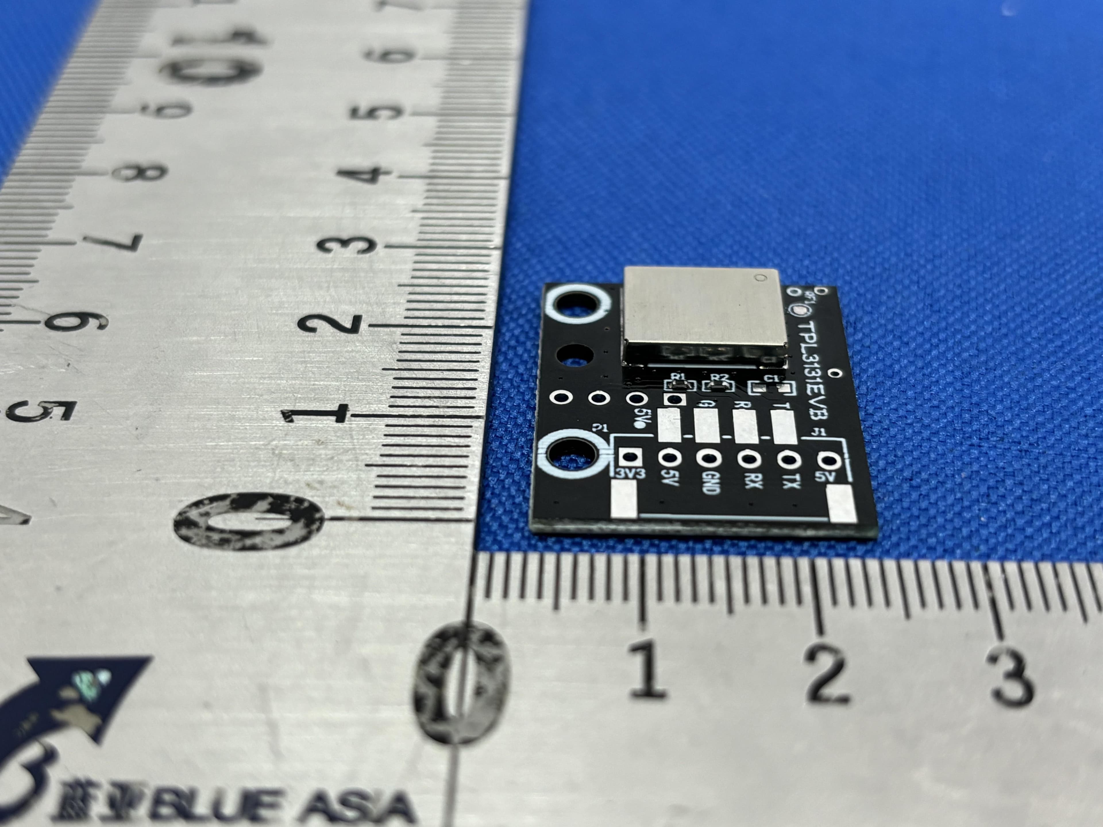
2BG7T-TPL3131
May 20, 2026Bluetooth module
Equipment Class
DTS - Digital Transmission System