A2DA9T1183GMobile Phone
Shenzhen Telacom Science & Technology Co., Ltd.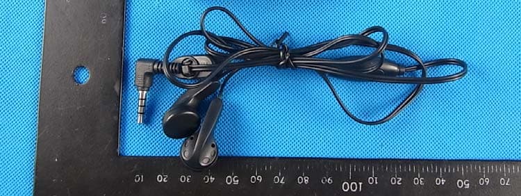
Click to zoom
Application Details
- Equipment Class
- PCE - PCS Licensed Transmitter held to ear
- Date of Grant
- Jun 04, 2012
- Application Purpose
- Original Equipment
- Date of Application
- Jun 04, 2012
- Equipment Note
- Mobile Phone
- Frequency Range
- 1852.40000000 - 1907.60000000
- Country
- China
Documents & Files
Document Text
Text extracted from the exhibit documents filed with the FCC. Open a document above to read the original.
Users Manual
T118 User manual 2 Contents 1 About your Mobile Phone ................................ 9 1.1 Appearance .............................................. 9 1.2 Key instructions ................................... 11 1.3 Icons ....................................................... 13 2 Getting started ................................................ 14 2.1 The Battery ......................................... 14 2.1.1 Install & remove a battery .. 14 2.1.2 Charging ................................ 15 2.2 SIM card installation ......................... 16 2.3 Memory card installation .................. 17 2.4 Storage Management ......................... 18 2.5 Power on and off ............................... 19 3 Call functions ..................................................... 19 3.1 Make a call ........................................... 19 3.1.1 Make a domestic call ............ 20 3.1.2 Make an extension call ......... 20 3.1.3 Make an international call .... 21 3.1.4 Make a call from Mobile Phone book 21 3 3.1.5 Redial a call by recent call lists 21 3.2 Answer a call ........................................ 21 3.3 Reject a call ......................................... 22 3.4 Call options ........................................... 22 4 Menu functions ................................................. 23 4.1 Messages ................................................ 23 4.1.1 Write message ...................... 23 4.1.2 Inbox .................................... 23 4.1.3 Drafts .................................. 24 4.1.4 Outbox ................................. 25 4.1.5 Broadcast Message ................ 25 4.1.6 Templates ............................. 26 4.1.7 Message Settings .................. 26 4.2 Multimedia ............................................ 27 4.2.1 Camera ................................. 27 4.2.2 Image viewer ........................ 27 4.2.3 Video recorder ...................... 28 4.2.4 Media player ......................... 28 4.2.5 Photo editor ........................ 29 4 4.2.6 Sound recorder ..................... 29 4.2.7 FM Radio ............................. 30 4.3 Extra ...................................................... 31 4.3.1 Calculator ............................. 31 4.3.2 Unit converter ..................... 31 4.3.3 Currency converter ............... 32 4.3.4 Answer machine .................... 32 4.4 Organizer ............................................... 32 4.4.1 Calendar................................ 32 4.4.2 Tasks .................................... 33 4.4.3 Alarm ................................... 33 4.4.4 World clock ........................... 33 4.4.5 Notes ................................... 33 4.4.6 Synchronization .................... 34 4.4.7 Phone sync ........................... 34 4.5 Settings ................................................. 34 4.5.1 Phone setting ....................... 34 4.5.2 Network setting ................... 35 4.5.3 Security Setting ................... 36 4.5.4 Connectivity ......................... 38 5 4.5.5 Restore Factory settings ...... 39 4.5.6 Sound effects ....................... 39 4.6 File Manager ......................................... 39 4.7 Phonebook ............................................. 40 4.7.1 Contacts ............................... 40 4.7.2 Add new contact .................. 41 4.7.3 Delete ALL ........................... 42 4.7.4 Copy All ............................... 42 4.7.5 Owner number ...................... 42 4.7.6 Preferred Storage ................ 42 4.7.7 Memory Status .................... 43 4.8 Call history ........................................... 43 4.9 Fun & Game ......................................... 43 4.9.1 SkyBuddy .............................. 43 4.9.2 Games .................................. 44 4.10 Service .................................................... 44 5 Battery information ........................................ 45 6 Safety information .......................................... 47 6.1 Operating environment ...................... 47 6.2 Electronic devices ................................ 47 6 6.2.1 Pacemaker ............................ 47 6.2.2 Hearing aids .......................... 48 6.2.3 Other medical devices ........... 48 6.2.4 Vehicles................................. 49 6.3 Potentially dangerous situations ..... 49 7 Care and maintenance ..................................... 50 8 FCC Caution ....................................................... 52 Preface Thank you very much for your choice of this product designed by our company! Our Mobile Phone complies with the Telecommunication industries standards of both the People's Republic of China and Europe. The product described in this guide is approved for use on the GSM networks, and has the GPRS functions. GSM network is a global cellular communications system of international standards. Allow you to receive an international telephone call used as in your homeland. However, before using these advanced network functions, 7 you must firstly apply for these required services. In order to better use your mobile phone, we suggest you to carefully read this statement to know all the functions well. Note: Due to the cellular network settings and the services provided, some functions may be unavailable, please query local service providers. For your safety Read these simple guidelines. Breaking the rules may be dangerous or illegal. Further detailed information is given in this manual. ROAD SAFETY Always keep your hands free to operate the vehicle while driving. Park the vehicle before using your Mobile Phone. SWITCH OFF IN AIRCRAFT Using of wireless telephones in aircraft may disrupt the operation of the aircraft. It is dangerous and illegal. Insure switching off the Mobile Phone before going aboard. SWITCH OFF IN HOSPITALS Follow any restrictions or rules. Switch off the Mobile Phone near medical equipment. 8 SWITCH OFF WHEN REFUELING Switch off the Mobile Phone at a refueling…
Text truncated - open the document above for the full version.
Block Diagram
ANT 26MHZ MT6276 BASEBAND H9DA1GH25HAMMR_4EM NAND Flash LCD IC Keypad MIC Speaker MT6162 RF Module SIM1 SIM2 RF7412 WCDMA PA RF 3232 GSM PA+RF Switch
Cover Letter(s)
Ersteller: D. Brandhorst Revision: 00 Erstelldatum: 07.03.2008 Datum: 00.00.00 Seite 1 von 1 PHOENIX TEST-LAB GmbH Product Certification Königswinkel 10 D 32825 Blomberg Date:2012-05-21 FCC ID: A2DA9T1183G Subject: Attestation Letter “Declaration of Conformity” Dear Sirs, Our products with the above FCC ID are defined as composite device. The transmitter is authorized under the “Certification” procedure. The device is also defined as “PC Periphery” acc to §15.101 Equipment authorization of unintentional radiators, where we hereby declare, that we apply and follow the “Declaration of Conformity” procedure. If you have any questions, please feel free to contact me at the address shown below. Yours sincerely, Signatory Signature Name: YanGuang Fu Title:Manager Company Name: Shenzhen Telacom Science & Technology Co., Ltd. Shenzhen Telacom Science & Technology Co., Ltd.
Cover Letter(s)
Shenzhen Telacom Science & Technology Co., Ltd. PHOENIX TEST-LAB GmbH Product Certification Königswinkel 10 D 32825 Blomberg Date: 21.05.2012 Authority to Act as an Agent We declare that the following representative (agent) Name Mark Wen Position General Manager Company Name Most Technology Service Co., Ltd. Address No.5, 2 nd Langshan Road, North District, Hi-Tech Industrial Park, Nanshan, Shenzhen, Guangdong, China Tel / Fax 86-755-86170306/86-755-86170310 E-Mail [email protected] to act on our behalf on all matters concerning the application and documents submitted to PHOENIX TEST-LAB for product certification below Product Name 3G Mobile Phone Model Name T118, K2776C Brand Name Cellacom /Telacom We also authorize BZT – TCP Certification GmbH, Ms.Wanida Patthanavoj (address: Hermann - Loens - Weg 6, 15859 Storkow b. Berlin Germany) to process the application. Yours sincerely, Signatory Name YanGuang Fu Position Manager Company Name Shenzhen Telacom Science & Technology Co., Ltd. Address 28/F Building B, The Pavilion Hotel, Huaqiangbei Road, Futian District, Shenzhen, Guangdong, China Tel / Fax 86) 755-61683916 /(86) 755-61683970 E-Mail [email protected] In case of FCC, we certify that we are not subject to a denial of Federal benefits, that include FCC benefits, pursuant to Section 5301 of the Anti-Drug Abuse Act of 1988, 21 U.S.C. §862 because of a conviction for possession or distribution of a controlled substance.
External Photos
APPENDIX-PHOTOGRAPHS OF EUT CONSTRUCTIONAL DETAILS Photo 1 Photo 2 Photo 3 Photo 4 Photo 5 Photo 6 Photo 7 Photo 8
ID Label/Location Info
W*L=4*4cm
Internal Photos
Photo 9 Photo 10 Photo 11
Internal Photos
Operational Description The transceiver is a complete RF front end for multi-band GSM , GPRS and WCDMA wireless communications. The receive section interfaces between the RF band-select SAW filters and the baseband subsystem. The receiver leverages a proven digital low-IF architecture and enables a universal baseband interface without the need for complex dc offset compensation. The transmit section provides a complete upconversion path from the baseband subsystem to the power amplifier (PA) using an offset phase-locked loop (OPLL) integrated with synthesizer technology. All sensitive components, such as TX/RF VCOs, loop filters, tuning inductors, and varactors are completely integrated into a single integrated circuit. The transceiver includes a digitally-controlled crystal oscillator (DCXO) and completely integrates the reference oscillator and varactor functionality. First power on the cell phone , ( Power supply’s voltage is set to 3.6 v-4.2 v, power is supplied to RF PA, audio PA circuit firstly.The pmu LDO will be opened once the power key is pressed.The LDO regulator power will be supplied to RF,FM,ATV,MCP,camera ect devices. Then the handset will detected if the sim card is existed or not.If existed ,the handset will attempt to register on the network The second SIM card’s function will be same as first SIM card. but only one of the dual SIM Card can be transmitting when the two SIM Cards are inserting the phone together. This 3G Mobile phone have Bluetooth function. Bluetooth 2.1+EDR Operation Frequency: 2402~2480 MHz Modulation Type: BT(1Mbps): GFSK BT EDR(2Mbps):∏/4-DQPSK BT EDR(3Mbps): 8-DPSK Bit Rate of Transmitter 1Mbps/2Mbps/3Mbps Number Of Channel 79 CH Antenna Designation: 0 dbi Output Power(Conducted): BT(1Mbps): 0.532dBm BT EDR(2Mbps): -0.064dBm BT EDR(3Mbps): -0.200dBm Frequency: GSM 850 PCS 1900 (U.S. Bands) GSM 900 DCS 1800 (Non-U.S. Bands) U.S. Bands: WCDMA FDD Band II WCDMA FDD Band V Non-U.S. Bands: WCDMA FDD Band I WCDMA FDD Band VIII Output Power: GSM850(Class 4) : 1.909 W (32.81dBm) GPRS850(Multislot Class 12) : 1.678 W (32.25 dBm) GSM1900 (Class 1) : 0.946 W (29.76dBm) GPRS1900 (Multislot Class 12) : 0.905W (29.57 dBm) WCDMA/HSDPA Band II: 0.214 W (23.32dBm) WCDMA/HSDPA BandV: 0.217W (23.37dBm) Type of Modulation GPRS/GSM Mode with GMSK Modulation WCDMA Mode with QPSK Modulation HSPA Mode with QPSK Modulation CIRCUIT DESCRIPTION 1、 Transmitter/Receiver Circuit This circuit shows the transmitter and receiver path of GSM/DCS/PCS and WCDMA2100/WCDAM850. The RF signal which is amplified by RF PA transmits to antenna through antenna switch andthan eradiate to the air.C117, L120, L119 make up of the antenna matching circuit.When receiver, the antenna receive the RF signal, and then demodulated by MT6276 after band filter. After inserting the battery, VRTC output voltage of 2V, and then the 32.768KHZ crystal start to work. Now press the power on/off switch SW105, then the inner program start initialing. Press the power on/off switch about 2s at normal work status, CPU MT6276 will detect the signal and start the power off program. The MT6276 integrate the charger control circuit. When inserting the charging Adapter, CHG_DEC detect high level, and start the charging program. The LCD connects to MT6276 through FPC. The signals are defined as follows: VDD: LCD inner driver voltage,provided by MT6276 RST:Reset signal WR0:LCD writing signal WR1:LCD reading signal CS0:LCD chip select signal CD: Register select D0~ D7:LCD data signal LCD backlight is Control by MT6276 GP30_PWM0_BLEN enable LCD backlight LED. The keypad contains SW107---SW118 SIM card pin defined as follows:VSIM:SIM card voltage supply, IO:Data input/output CLK:Clock signal RST:Reset signal The I/O circuit contains earphone port, UART port, charge input.HP is detecting pin for earphone insert. For normal it is high, and become low when earphone insert. The Bluetooth chip is MT6276 include, and the working frequency is 2400-2483.5MHz
Operational Description
Operational Description The transceiver is a complete RF front end for multi-band GSM , GPRS and WCDMA wireless communications. The receive section interfaces between the RF band-select SAW filters and the baseband subsystem. The receiver leverages a proven digital low-IF architecture and enables a universal baseband interface without the need for complex dc offset compensation. The transmit section provides a complete upconversion path from the baseband subsystem to the power amplifier (PA) using an offset phase-locked loop (OPLL) integrated with synthesizer technology. All sensitive components, such as TX/RF VCOs, loop filters, tuning inductors, and varactors are completely integrated into a single integrated circuit. The transceiver includes a digitally-controlled crystal oscillator (DCXO) and completely integrates the reference oscillator and varactor functionality. First power on the cell phone , ( Power supply’s voltage is set to 3.6 v-4.2 v, power is supplied to RF PA, audio PA circuit firstly.The pmu LDO will be opened once the power key is pressed.The LDO regulator power will be supplied to RF,FM,ATV,MCP,camera ect devices. Then the handset will detected if the sim card is existed or not.If existed ,the handset will attempt to register on the network The second SIM card’s function will be same as first SIM card. but only one of the dual SIM Card can be transmitting when the two SIM Cards are inserting the phone together. This 3G Mobile phone have Bluetooth function. Bluetooth 2.1+EDR Operation Frequency: 2402~2480 MHz Modulation Type: BT(1Mbps): GFSK BT EDR(2Mbps):∏/4-DQPSK BT EDR(3Mbps): 8-DPSK Bit Rate of Transmitter 1Mbps/2Mbps/3Mbps Number Of Channel 79 CH Antenna Designation: 0 dbi Output Power(Conducted): BT(1Mbps): 0.532dBm BT EDR(2Mbps): -0.064dBm BT EDR(3Mbps): -0.200dBm Frequency: GSM 850 PCS 1900 (U.S. Bands) GSM 900 DCS 1800 (Non-U.S. Bands) U.S. Bands: WCDMA FDD Band II WCDMA FDD Band V Non-U.S. Bands: WCDMA FDD Band I WCDMA FDD Band VIII Output Power: GSM850(Class 4) : 1.909 W (32.81dBm) GPRS850(Multislot Class 12) : 1.678 W (32.25 dBm) GSM1900 (Class 1) : 0.946 W (29.76dBm) GPRS1900 (Multislot Class 12) : 0.905W (29.57 dBm) WCDMA/HSDPA Band II: 0.214 W (23.32dBm) WCDMA/HSDPA BandV: 0.217W (23.37dBm) Type of Modulation GPRS/GSM Mode with GMSK Modulation WCDMA Mode with QPSK Modulation HSPA Mode with QPSK Modulation CIRCUIT DESCRIPTION 1、 Transmitter/Receiver Circuit This circuit shows the transmitter and receiver path of GSM/DCS/PCS and WCDMA2100/WCDAM850. The RF signal which is amplified by RF PA transmits to antenna through antenna switch andthan eradiate to the air.C117, L120, L119 make up of the antenna matching circuit.When receiver, the antenna receive the RF signal, and then demodulated by MT6276 after band filter. After inserting the battery, VRTC output voltage of 2V, and then the 32.768KHZ crystal start to work. Now press the power on/off switch SW105, then the inner program start initialing. Press the power on/off switch about 2s at normal work status, CPU MT6276 will detect the signal and start the power off program. The MT6276 integrate the charger control circuit. When inserting the charging Adapter, CHG_DEC detect high level, and start the charging program. The LCD connects to MT6276 through FPC. The signals are defined as follows: VDD: LCD inner driver voltage,provided by MT6276 RST:Reset signal WR0:LCD writing signal WR1:LCD reading signal CS0:LCD chip select signal CD: Register select D0~ D7:LCD data signal LCD backlight is Control by MT6276 GP30_PWM0_BLEN enable LCD backlight LED. The keypad contains SW107---SW118 SIM card pin defined as follows:VSIM:SIM card voltage supply, IO:Data input/output CLK:Clock signal RST:Reset signal The I/O circuit contains earphone port, UART port, charge input.HP is detecting pin for earphone insert. For normal it is high, and become low when earphone insert. The Bluetooth chip is MT6276 include, and the working frequency is 2400-2483.5MHz
RF Exposure Info
Compliance Certification Services Inc. Reference No .: KS120516A01-SE Date of Issue: May 23,2012 Report No .: KS120516A01-SE Page 1 of 39 GSM 850-Right Head Cheek Low CH128........................................................................................ 2 GSM 850-Right Head Cheek Middle CH190.................................................................................... 3 GSM 850-Right Head Cheek High CH251........................................................................................ 4 GSM 850-Right Head Tilted High CH251......................................................................................... 5 GSM 850-Left Head Cheek High CH251.......................................................................................... 6 GSM 850-Left Head Tilted High CH251............................................................................................ 7 PCS-1900-Right Head Cheek Low CH512....................................................................................... 8 PCS-1900-Right Head Cheek Middle CH661.................................................................................. 9 PCS-1900-Right Head Cheek High CH810.................................................................................... 10 PCS-1900-Right Head Tilted High CH810......................................................................................11 PCS 1900-Left Head Cheek High CH810....................................................................................... 12 PCS 1900-Left Head Tilted High CH810........................................................................................ 13 GSM 850-Body Up High CH251....................................................................................................... 14 GSM 850-Body Down Low CH128................................................................................................... 15 GSM 850-Body Down Middle CH190.............................................................................................. 16 GSM 850-Body Down High CH251.................................................................................................. 17 GPRS 850-Body Up High CH251..................................................................................................... 18 GPRS 850-Body Down High CH251............................................................................................... 19 PCS1900-Body Up High CH810....................................................................................................... 20 PCS1900-Body Down High CH810................................................................................................. 21 GPRS1900-Body Up High CH810.................................................................................................... 22 GPRS1900-Body Down High CH810.............................................................................................. 23 WCDMA Band II-Right Head Cheek Low CH9262....................................................................... 24 WCDMA Band II-Right Head Cheek Middle CH9400.................................................................. 25 WCDMA Band II-Right Head Cheek High CH9538...................................................................... 26 WCDMA Band II-Right Head Tilted Low CH9262........................................................................ 27 WCDMA Band II-Left Head Cheek Low CH9262.......................................................................... 28 WCDMA Band II-Left Head Tilted Low CH9262........................................................................... 29 WCDMA Band V-Right Head Cheek Low CH4132....................................................................... 30 WCDMA Band V-Right Head Cheek Middle CH4182.................................................................. 31 WCDMA Band V-Right Head Cheek High CH4233...................................................................... 32 WCDMA Band V-Right Head Tilted Low CH4132........................................................................ 33 WCDMA Band V-Left Head Cheek Low CH4132......................................................................... 34 WCDMA Band V-Left Head Tilted Low CH4132........................................................................... 35 WCDMA Band II-Body Up Low CH9262......................................................................................... 36 WCDMA Band II-Body Down Low CH9262................................................................................... 37 WCDMA Band V-Body Up Low CH4132........................................................................................ 38 WCDMA Band V-Body Down Low CH4132................................................................................... 39 Compliance Certification Services Inc. Reference No .: KS120516A01-SE Date of Issue: May 23,2012 Report No .: KS120516A01-SE Page 2 of 39 Test Laboratory: Compliance Certification Services Inc. May 22, 2012 GSM 850-Right Head Cheek Low CH128 DUT: 3G Mobile Phone; Type: T118; Serial: 358688000000158 Communication System: Generic GSM; Communication System Band: GSM 850 (824.0 - 849.0 MHz); Frequency: 824.2 MHz;Communication System PAR: 9.03 dB Ambient: Temperature: 21 °C Relative humidity: 58% Liquid : Temperature: 20 °C Medium parameters used (interpolated): f = 824.2 MHz; σ = 0.88 mho/m; ε r = 41.628; ρ = 1000 kg/m 3 Phantom section: Right Section Measurement Standard: DASY5 (IEEE/IEC/ANSI C63.19-2007) DASY Configuration: • Probe: EX3DV4 - SN3755; ConvF(8.99, 8.99, 8.99); Calibrated: 1/20/2012 • Sensor-Surface: 2.5mm (Mechanical Surface Detection) • Electronics: DAE4 Sn1245; Calibrated: 1/11/2012 • Phantom: Twin SAM Phantom; Type: QD 000 P40 CD; Serial: 1609 • DASY52 52.8.0(692); SEMCAD X 14.6.4(4989) GSM850/Right Head Cheek Low CH128/Area Scan (6x10x1): Measurement grid: dx=15mm, dy=15mm Maximum value of SAR (measured) = 0.513 mW/g GSM850/Right…
Text truncated - open the document above for the full version.
Schematics
2012-1-10 K2776 P0 SHEET: 1 8 GSM Telacom A2 1:1 REV: SIZE: DATE: COMPANY: TITLE: DRAWING NO: SCALE: A B C D 1 2 3 4 5 6 D C B A 1 2 3 4 5 6 OF P0-->P1: 1.ADD C21, R13,R14 20120301 1.L107=22nH,C121=C124=3.9pF,L106=15nH,C185=5.6nH,C184=22pF,L131=6.8nH 2.DNP:C9=C10=C11=33pF,C8=1uF,J103=CAF99-06153-1503 2012-1-10 GSM K2776 P0 OF 6 5 4 3 2 1 A B C D 6 5 4 3 2 1 D C B A SCALE: DRAWING NO: TITLE: COMPANY: DATE: SIZE: REV: 1:1 A2 Telacom 8 2 SHEET: GSM W_BAND1 PA W_BAND_5 PA Note : Reserve for debug Note : Reserve for debug Note : Use RX Co-banding GSM850 = 3G B5 GSM900 = 3G B8 GSM1900= 3G B2 900MHz 850MHz 1800MHz 1900MHz B1/B2/B4 1 MK108 MARK 1 SHD103 K2776-BB-SHD 1 SHD102 K2776-RF-SHD L119 DNP L120 DNP 6 5 2 1 3 4 CON101 TST_PORT_0A MM8430-2600B C177 0R R146 0R R144 NCP15WF104F03RC R143 39k R145 220k 1 VCC1 2 RF_IN 3 VMODE1/VBP 4 VMODE0 5 VEN 6 CPL 7 GND 8 GND/ISO 9 RF_OUT 10 VCC2 11 GND U102 BAND 2 PA C217 220pF C215 33pF R142 DNP C213 DNP C214 220pF L104 DNP C216 1uF 1 VCC1 2 RF_IN 3 VMODE1/VBP 4 VMODE0 5 VEN 6 CPL 7 GND 8 GND/ISO 9 RF_OUT 10 VCC2 11 GND U103 ACPM5405 C131 4.7uF C132 220pF C133 56pF C134 33p L105 DNP R116 51R C136 220pF L106 15nH C137 1uF C103 56pF R133 DNP R109 24R R136 24R L127 NM C198 1nF C180 1uF L124 NM C186 1.5nH C183 1.5nH C187 DNP C193 1nF 8 RX 5 G 1 RX 2 G 3 TX 4 G 7 G 6 ANT 9 G U111 B7955 C192 1nF C181 1uF 8 RX 5 G 1 RX 2 G 3 TX 4 G 7 G 6 ANT 9 G U109 SAYRJ836MCA0F00/B7923 C196 2.2pF C197 2.2pF L126 NM C189 3.9nH C184 22pF C195 NM C191 0.5pF C199 3.9pF R128 0R C194 100nF L130 2.7nH C178 1uF L125 47nH C182 1uF L129 2.7nH C190 DNP A6 RESET A8 XO1_/_REF_IN A10 CLK_MODE B9 VTUNE B11 VSUP2B C2 EN C18 TX_IP D1 VINT E2 DATA1 E18 TX_QP F1 DATA0 F17 TX_HB3 M17 VSUP3 N18 VDD_28A P17 DC_TEST_OP R18 RF_TEST_OP T17 NC U4 LNA2N U6 LNA3N U8 LNA4N U10 LNA5N U12 LNA6N U14 LNA7N U16 LNA8P V3 LNA1P V9 LNA4P V11 LNA5P V13 LNA6P V15 LNA7P V17 LNA8N A2 REFCLK1 A12 GND B15 GND B17 TX_IN D17 TX_QN G2 CLK G18 TX_HB2 H17 TX_HB1 J2 VSUP2A J18 TX_LB2 K1 VDD_18 K17 TX_LB1 L2 VSUP1 L18 GND A4 REFCLK3 A14 GND A16 GND B1 GND B3 REFCLK2 B5 VDDXO B7 XO2 B13 PDET M1 RX_BBQN N2 RX_BBQP P1 RX_BBIN R2 RX_BBIP T1 GND U2 LNA1N U18 GND V5 LNA2P V7 LNA3P 63 GND H1 VDD_28B U110 MT6162 C179 1uF C185 5.6nH C188 1.0nH 2 NC 1 VCONTROL 3 GND 6 VCC 5 NC 4 OUT U112 KT2520F26000DCW28EAK/7L26002007S2/TX0371B C207 33nH C205 0R R132 DNP R131 0R C208 18pF C202 NM R140 24K C204 NM R138 10K C203 NM C201 22uF RF3232DS 1 GND 2 GND 23 GND 4 GND 15 GND 6 GND 7 GND 8 GND 9 GND 16 GND 3 RF_IN_LB 5 RF_IN_HB 10 RX1 11 RX2 12 TRX1 13 TRX2 14 ANT 20 GPCTRL0 17 GPCTRL2 19 GPCTRL1 21 TXEN 22 VRAMP 18 VBATT U101 RF3232DS C111 220nF R137 DNP C206 56pF R111 0R C113 NM C209 6pF C210 220pF C114 3.9pF C119 3.9pF C121 3.9pF C124 3.9pF L108 15nH L107 22nH C126 3pF C127 3pF L109 6.8nH C161 3pF C129 3pF L110 6.8nH L121 3.3nH L122 3.3nH L123 6.8nH L102 DNP C130 33pF L103 DNP R113 36R C125 2.2nH C128 0.5pF ANT2 ANT-3X2 ANT1 ANT-3X2 2 G 1 IN_1 8 OUT_1 9 OUT_1 3 G 4 IN_2 5 G 10 G 6 OUT_2 7 OUT_2 Z101 SFRM81DY102 2 G 1 IN_1 8 OUT_1 9 OUT_1 3 G 4 IN_2 5 G 10 G 6 OUT_2 7 OUT_2 Z102 SFWG42MY002/B9514/FAR-G6KT-1G9600-Y4RU 1 MK101 MARK C1 DNP C135 56pF L128 DNP ANT3 ANT-3X2 B1 GZ1005U102T(f) B2 GZ1005U102T(f) B3 GZ1005U102T(f) B4 GZ1005U102T(f) C12 DNP 1 2 R10 0R 1 MK1 TAG GND GND GND GND VTCXO ADC7_UMTS_TEMP [3] VM1 [2,3] VM0 [2,3] W_PA1_ON [3] W_PA1_ON W_PA_B1_IN [2] W_PA_OUT_B1 [2] VM1 [2,3] VM0 [2,3] W_PA5_ON [3] W_PA5_ON W_PA_LB_IN [2] W_PA_OUT_B5 [2] PDET_B5 [2] GND VBAT VBAT GND W_PA_OUT_B1 [2] W_PA_OUT_B5 [2] GSM1800 [2] W_PA_B1_IN [2] W_PA_B2_IN [2] GGE_PA_HB_IN [2] GGE_PA_LB_IN [2] W_PA_LB_IN [2] VRF18 VRF28 BSI1_DATA [3] GSM_UMTSTX_IP [3] GSM_UMTSTX_IN [3] GSM_UMTSTX_QP [3] GSM_UMTSTX_QN [3] BSI1_CS1 [3] UMTSRX_IP [3] UMTSRX_IN [3] UMTSRX_QP [3] UMTSRX_QN [3] BSI1_CS0 [3] BSI1_CLK [3] AFC [3] VTCXO VTCXO VDD18 TRX1 [2] TRX2 [2] TRX1 [2] GGE_PA_HB_IN [2] GGE_PA_LB_IN [2] VBAT VAPC [3] PAEN [3] ASM_VCT3 [3] ASM_VCT4 [3] ASM_VCT1 [3] GSM900 [2] GSM1800 [2] TRX2 [2] W/GSM_ANT [2] GSM850P [2] GSM850N [2] GSM900P [2] GSM900N [2] DCS1900P [2] DCS190]0N [2] PCS1800P [2] PCS1800N [2] GND GND GSM850P [2] GSM850N [2] GSM900P [2] GSM900N [2] DCS1900P [2] DCS190]0N [2] PCS1800N [2] PCS1800P [2] GSM900 [2] SYSCLK [3,5] W_PA_B2_IN [2] WP_DET [2] VBAT VBAT GND PDET_B5 [2] GND GND GND GND GND GND GND W/GSM_ANT [2] WP_DET [2] GND W_PA_B1_IN [2] OH_REFCLK3 OF 6 5 4 3 2 1 A B C D 6 5 4 3 2 1 D C B A SCALE: DRAWING NO: TITLE: COMPANY: DATE: SIZE: REV: 1:1 A2 Telacom GSM 8 3 SHEET: K2776 P0 2012-1-10 5 8 10 10 3 MSDC A C D 5 4 3 2 1 D B A 1 2 4 5 9 2 Close to MT6276 Close to MT6276 Close to MT6276 Close to MT6276 1.35V Close to MT6276 Close to MT6276 Close to MT6276 4 5 1.8V 1.8V 1.8V GPIO22-52 =1.8V 1.8V 1.8V 1.8V 1.8V 1.8V C212 22pF C211 22pF AL14 DL_I_P AM15 DL_I_N AP15 DL_Q_P AR16 DL_Q_N AK17 UL_I_P AJ18 UL_I_N AM17 UL_Q_P AL16 UL_Q_N AN22 APC AH19 AFC AP21 3G_TX_VGA AK19 3G_VBIAS AM25 BSI1_CLK AL22 BSI1_DATA AK23 BSI1_CS1/GP1/PD AN24 BSI1_CS0 AN26 BSI0_CLK AR28 BSI0_DATA AL26 BSI0_CS0 AP27 BSI0_CS1/GP2/PD AK29 BPI_BUS0 AG24 BPI_BUS1 AE24 BPI_BUS2 AM31 BPI_BUS3 AN32 BPI_BUS4 AJ28 BPI_BUS5 AL28 BPI_BUS6/GP7/PD AM29 BPI_BUS7/GP8/PD AL30 BPI_BUS8/GP10/PD AP31 BPI_BUS9/GP6/PD AR32 BPI_BUS10 AJ26 BPI_BUS11 AN28 BPI_BUS12 AR30 BPI_BUS13/GP5/PD AN30 BPI_BUS14/GP9/PD AM27 VM0/GP3/PD AP29 VM1/GP4/PD U104-A MT6276 AM21 26M_CK_IN AR22 XOUT AP23 XIN AM23 TESTMODE AK21 RTC_GPIO/GP109/PD AP33 URXD1/GP11/PU AR34 UTXD1/GP12 AG30 MCU_JTRST_B/GP22/PD AJ32 MCU_JTCK/GP23/PU AE28 MCU_JTDI/GP24/PU AM35 MCU_JTMS/GP25/PU AD25 MCU_JTDO/GP26 AL34 MCU_JRTCK/GP27 AF29 SWCLKTCK/GP28/PU AK33 SWDIOTMS/GP29/PU E32 LSCK/GP70/PD G30 LSA0/GP71/PD D31 LSDA/GP72/PD G32 LSCE0B/GP73 B31 LSCE1B/GP74/PU AH27 URXD2/GP13/PU AN34 UTXD2/GP14 W4 USB_VBUS P1 USB_DM R2 USB_DP T7 USB_VRT U8 USB_ID U2 STXP V1 STXN V7 MPX AC30 SRCLKENA AH31 EINT0/GP33/PU AG32 EINT1/GP34/PU AF31 EINT2/GP35/PU AP35 DAICLK/GP15/PD AM33 DAIPCMOUT/GP16/PD AL32 DAIPCMIN/GP17/PD AG28 DAISYNC/GP18/PD AH29 DAIRST/GP19/PD AH33 PWMA/GP…
Text truncated - open the document above for the full version.
Test Report
FCC RADIO TEST REPORT FCC ID: A2DA9T1183G Product: 3G Mobile Phone Trade Name: Cellacom /Telacom Model Name: T118 Serial Model: K2776C Report No.: MTE/EAH/D12050598 Prepared for Shenzhen Telacom Science & Technology Co., Ltd. 28/F Building B, The Pavilion Hotel, Huaqiangbei Road, Futian District, Shenzhen, Guangdong, China Prepared by Most Technology Service Co., Ltd. No.5, Langshan 2nd Rd., North Hi-Tech Industrial park, Nanshan, Shenzhen, Guangdong, China Tel.: 86-755-8617 0306 Fax.: 86-755-8617 0310 Page 2 of 55 Report No.: MTE/EAH/D12050598 ` TEST RESULT CERTIFICATION Applicant’s name ................. : Shenzhen Telacom Science & Technology Co., Ltd. Address ................................. : 28/F Building B, The Pavilion Hotel, Huaqiangbei Road, Futian District, Shenzhen, Guangdong, China Manufacture's Name ............ : Finmek Electronic (Shenzhen) Co., Ltd. Address ................................. : 5/F, South Block 23, Shatoukok Free Trade Zone, Shenzhen, China Product description Product name ........................... : 3G Mobile Phone Model and/or type reference : T118 Serial Model: K2776C Rating(s) ................................ : DC 3.7V Standards ............................. : 47 CRF Part2 47 CRF Part22 subpart H 47 CRF Part24 subpart E Test procedure ............................... : ANSI C63.4-2003 This device described above has been tested by MOST, and the…
Text truncated - open the document above for the full version.
Contact Information
Applicant
YanGuang Fu(Manager)
Test Firm
Most Technology Service Co., Ltd.Mark Wen
Technical Specifications
| # | Rule Parts | Frequency Range | Power Output | Emission | Tolerance |
|---|---|---|---|---|---|
| 4 | 24E | 1.85 GHz - 1.91 GHz | 123.00 mW | 4M20F9W | 0.06 ppm |
Other Applications from Shenzhen Telacom Science & Technology Co., Ltd.
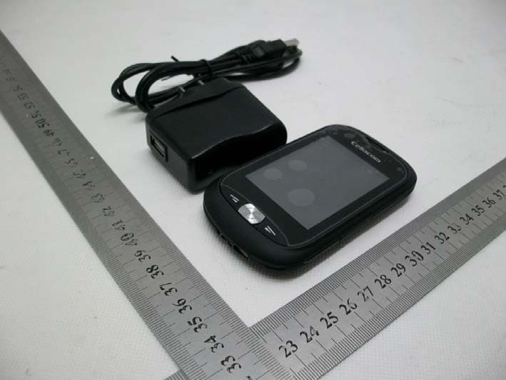
A2DA2T303G
Apr 01, 2013GSM Mobile Phone
Equipment Class
PCE - PCS Licensed Transmitter held to ear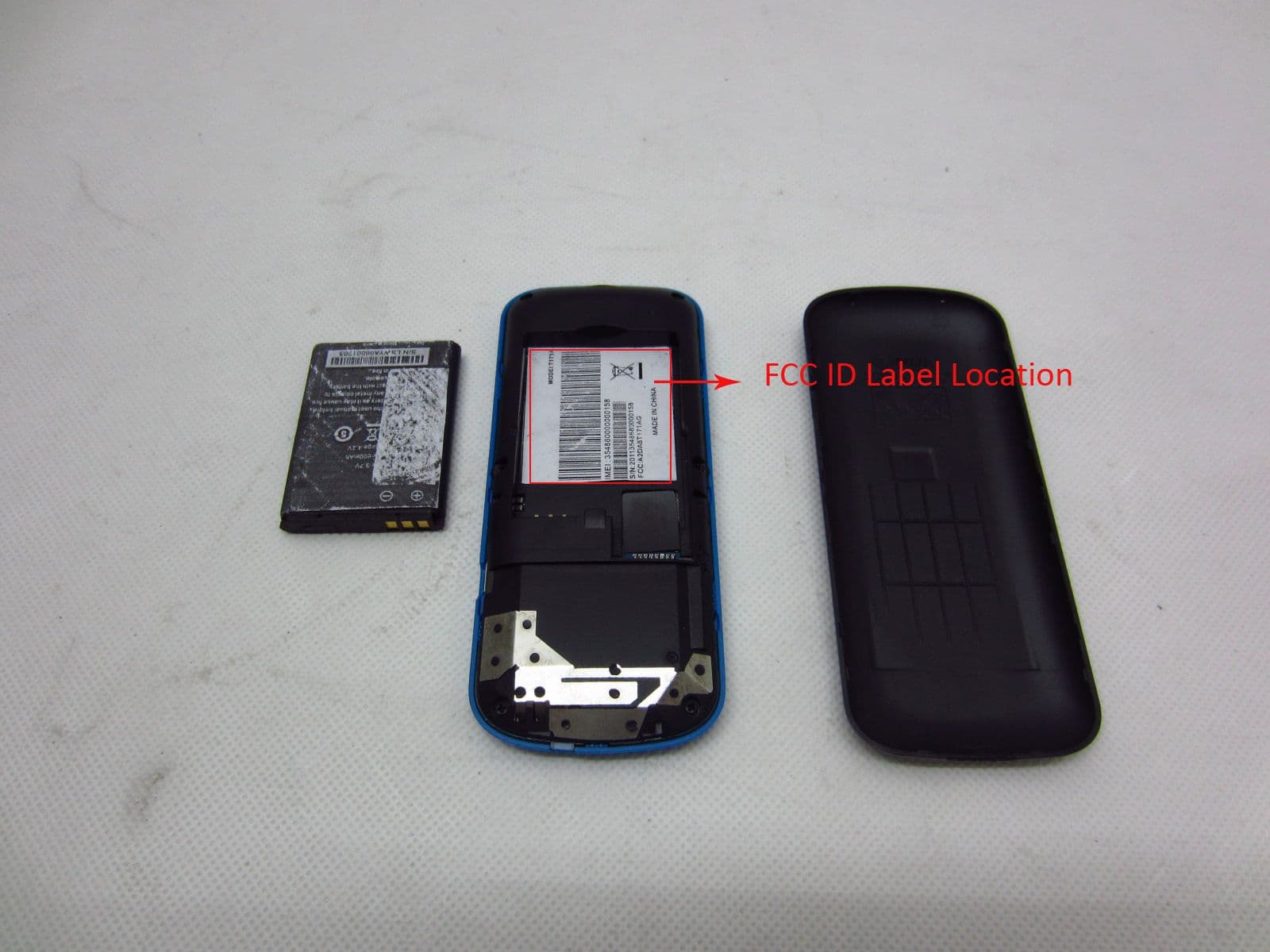
A2DA8T171AG
Mar 07, 2013GSM Mobile Phone
Equipment Class
JBP - Part 15 Class B Computing Device Peripheral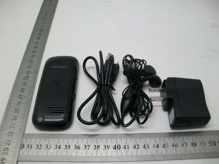
A2DA2T285G
Jan 23, 2013GSM Mobile Phone
Equipment Class
PCE - PCS Licensed Transmitter held to ear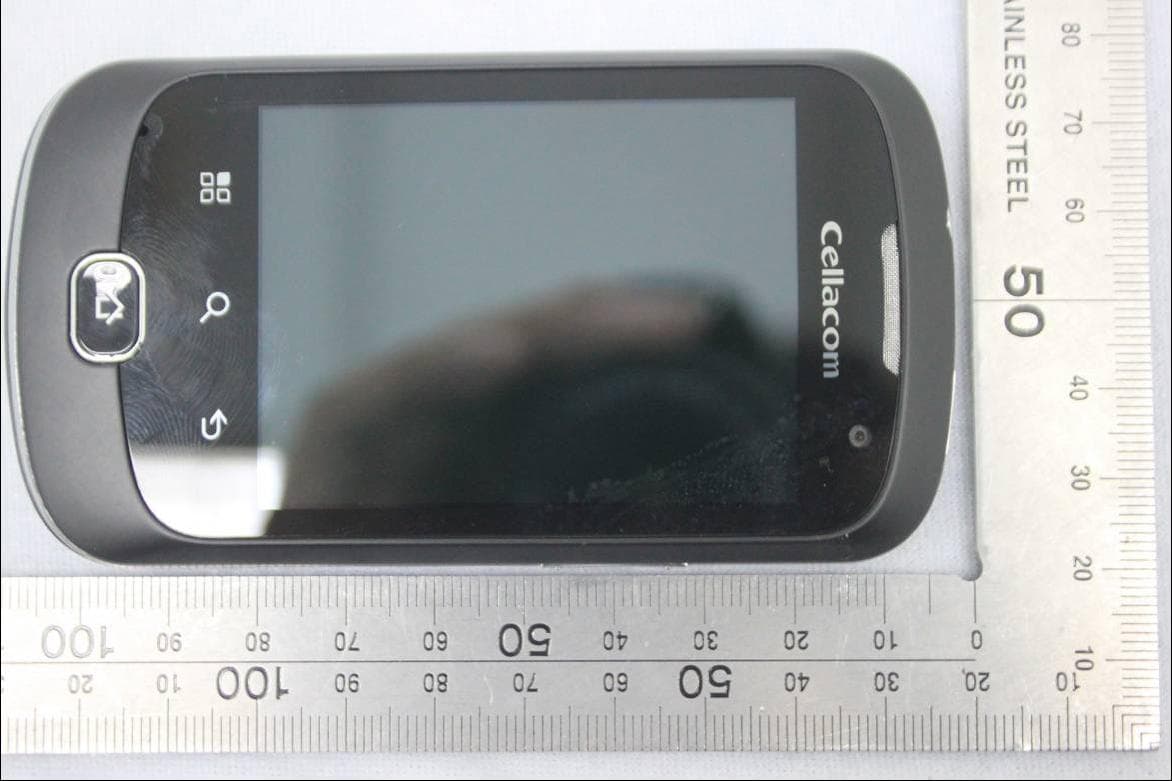
A2DA9T7013G
Nov 05, 20123G Mobile Phone
Equipment Class
DTS - Digital Transmission System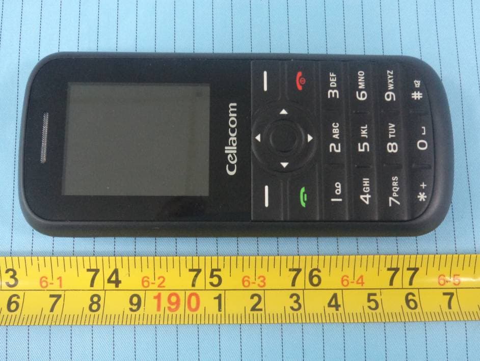
A2DA8T171G
Apr 16, 2012GSM Mobile Phone
Equipment Class
PCE - PCS Licensed Transmitter held to ear