A2SCR108MOBILE PHONE
Cellrunners Distribution Corporation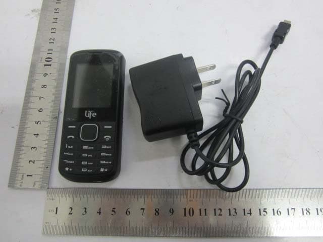
Click to zoom
Application Details
- Equipment Class
- PCE - PCS Licensed Transmitter held to ear
- Date of Grant
- Dec 05, 2011
- Application Purpose
- Original Equipment
- Date of Application
- Dec 05, 2011
- Equipment Note
- MOBILE PHONE
- Frequency Range
- 1850.20000000 - 1909.80000000
- Country
- United States
Documents & Files
Document Text
Text extracted from the exhibit documents filed with the FCC. Open a document above to read the original.
Users Manual
Color-screen Call Phone User’s Manual Contents 1 General Information .......................................................................................................................2 1.1 Introduction .........................................................................................................................2 1.2 Safety ..................................................................................................................................3 1.3 Warning and Notice.............................................................................................................3 1.3.1 Basic Notices................................................................................................................... 3 1.3.2 Notices of Your Phone .....................................................................................................3 1.3.3 Notices of Battery Use..................................................................................................... 4 1.3.4 Notices of Charger Use ...................................................................................................5 1.3.5 Care and Maintenance .................................................................................................... 5 1.3.6 General Notices............................................................................................................... 6 2 Getting Started ...............................................................................................................................6 2.1 Overview and Introduction .................................................................................................6 Product Specification ............................................................................................................... 6 2.2 Keypad ................................................................................................................................7 2.3 Battery .................................................................................................................................7 2.4 Network Connections..........................................................................................................8 2.4.1 SIM Card ......................................................................................................................... 8 2.4.2 Insert and Remove the SIM Card .................................................................................... 8 2.4.3 Turn Your Phone On or Off ............................................................................................. 8 2.4.4 Phone unlock................................................................................................................... 8 2.4.5 Unlock the SIM Card.......................................................................................................8 2.4.6 Connect to the Network ...................................................................................................9 2.4.7 Make Calls ...................................................................................................................... 9 2.4.8 Make Domestic Calls ......................................................................................................9 2.4.9 Dial Extension................................................................................................................. 9 2.4.10 International telephone Calls...................................................................................... 10 2.4.11 Dial the Numbers of Phonebook.................................................................................. 10 2.4.12 Emergency Number ..................................................................................................... 10 2.4.13 Answer Calls ............................................................................................................... 10 2.4.14 Call Records .................................................................................................................11 2 2.4.15 Call Menu.....................................................................................................................11 3 Function Menus............................................................................................................................ 11 3.1 Use of Function Menus ..................................................................................................... 11 Scroll Searching and Selection Function ................................................................................11 Exit Menus...............................................................................................................................11 3.2 Phonebook......................................................................................................................... 11 3.3 Messages ...........................................................................................................................12 3.3.1 Write Message ................................................................................................12 3.3.2 Inbox ..............................................................................................................12 3.3.3 Outbox............................................................................................................12 3.3.4 Settings...........................................................................................................12 3.3.5 Memory Status ...............................................................................................13 3.3.6 Voice mail.......................................................................................................13 3.3.7 Broadcast Messages .......................................................................................13 3.4 Call Logs ........................................................................................................................…
Text truncated - open the document above for the full version.
Cover Letter(s)
Cellrunners Distribution Corporation 1701 Green Road Suite H, Pompano Beach, FL 33064, USA FCC ill: A2SCR108 POWER OF ATTORNEY November 23, 2011 Federal Communications Commission Authorization and Evaluation Division 7435 Oakland Mills Road Columbia, MD 21046 To Whom It May Concern: We, the undersigned, hereby authorize SEM.Test Compliance Service Co., Ltd. Jandy So on our behalf, to apply to the Federal Communications Commission on our equipment. Any and all acts carried out by SEM.Test Compliance Service Co., Ltd. Jandy So on our behalf shall have the same effect as acts of our own. This is to advise that we are in full compliance with the Anti-Drug Abuse Act. We, Cellrunners Distribution Corporation are not subject to a denial of federal benefits pursuant to Section 5301 of the Anti-Drug Act of 1988, 21 USC853a, and no party to the application is subject to a denial of federal benefits pursuant to that section. Sincerely, :l " / /~, , ' __ ~~___________________~_~_=-~-r Matthew Mocarski President
External Photos
Cellrunners Distribution Corporation Model: CR108 REPORT NO.: STR11118225I FCC PART 22H/24E EXHIBIT 2 - EUT EXTERNAL PHOTOGRAPHS EUT View 1 EUT View 2 Cellrunners Distribution Corporation Model: CR108 REPORT NO.: STR11118225I FCC PART 22H/24E EUT View 3 EUT View 4
ID Label/Location Info
Cellrunners Distribution Corporation Model: CR108 REPORT NO.: STR11118225I FCC PART 22H/24E EXHIBIT 1- PRODUCT LABELING Proposed FCC ID Label Format FCC ID: A2SCR108 Specifications : Text is Black in color and justified. Labels are printed in indelible ink on permanent adhesive silk-screened onto the EUT or shall be affixed at a conspicuous location on the EUT. Proposed Label Location on EUT FCC ID Label Location
ID Label/Location Info
Cellrunners Distribution Corporation Model: CR108 REPORT NO.: STR11118225I FCC PART 22H/24E EXHIBIT 1- PRODUCT LABELING Proposed FCC ID Label Format FCC ID: A2SCR108 Specifications : Text is Black in color and justified. Labels are printed in indelible ink on permanent adhesive silk-screened onto the EUT or shall be affixed at a conspicuous location on the EUT. Proposed Label Location on EUT FCC ID Label Location
Internal Photos
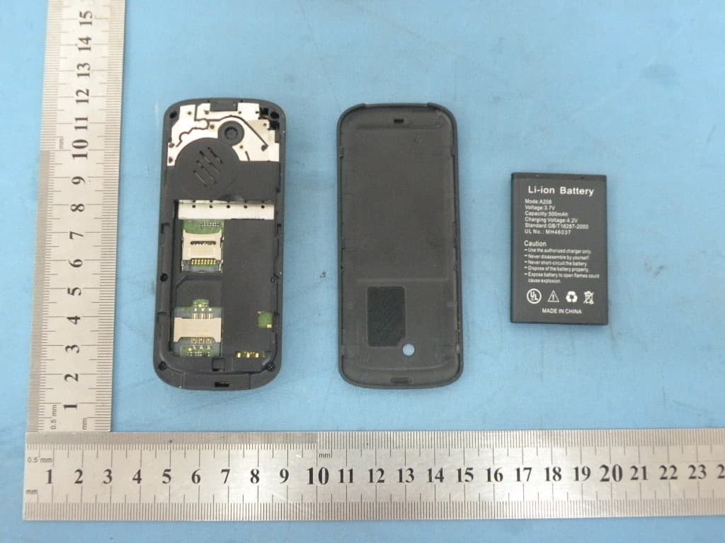
Cellrunners Distribution Corporation Model: CR108 REPORT NO.: STR11118225I FCC PART 22H/24E EXHIBIT 3 - EUT INTERNAL PHOTOGRAPHS EUT Housing and Board View 1 EUT Housing and Board View 2 Cellrunners Distribution Corporation Model: CR108 REPORT NO.: STR11118225I FCC PART 22H/24E Solder Board-Component View 1 Solder Board-Component View 2 Cellrunners Distribution Corporation Model: CR108 REPORT NO.: STR11118225I FCC PART 22H/24E Solder Board-Component View 3 Solder Board-Component View 4 Cellrunners Distribution Corporation Model: CR108 REPORT NO.: STR11118225I FCC PART 22H/24E Solder Board-Component View 5
Operational Description
Circuit Description 1. Scope This document shows and provides the more detail information about the platform we used. The basic description for the Baseband and RF section are also included.The baseband circuit is based on MTK and RF circuit is based on RFMD. It works at two bands, GSM850, PCS1900 band. 2. Baseband MT6252 is MTK first monolithic GSM handset chip solution which integrated RF, analog baseband,digital baseband as well as power Management Unit(PMU)and can greatly reduce the component count and make smaller PCB size. Beside, MT6252 is capable of SAIC(Single Antenna Interference Cancellation)and AMR speech. Based on 32 bit ARM7EJ-S RISC processor,MT6252 provides an unprecedented platform for high quality modem performance. Platform MT6252 has the ARM7EJ-S RISC processor running up to 104 MHz,thus providing best trade-off between system performance and power consumption. For large amount of data transfer,high performance DMA(Direct Memory Access) with hardware flow control is implemented,that which greatly enhances the data movement speed while reducing MCU processor load. Targeted as a modem-centric platform for mobile application,MT6252 also provides hardware security digital rights management for copyright protection. For further safeguarding,and to protect manufacturer’s development investment,hardware flash content protection is also provide to prevent unauthorized porting of software. Audio Interface Using a highly integrated mixed-signal Audio Front-End, the MT6252 architecture allows for easy audio interfacing with direct connection to the audio transducers. The audio interface integrates D/A and A/D Converters for Voice band, as well as high resolution Stereo D/A Converters for Audio band. In addition, MT6252 also provides Stereo Input and Analog Mux. MT6252 supports AMR codec to adaptively optimize speech and audio quality. Moreover, HE-AAC codec is implemented to deliver CD-quality audio at low bit rates. Overall, MT6252’s audio features provide a rich platform for multi-media applications. Radio Interface MT6252 integrates a mixed-signal Baseband front-end in order to provide a well-organized radio interface with flexibility for efficient customization. It contains gain and offset calibration mechanisms, and filters with programmable coefficients for comprehensive compatibility control on RF modules. MT6252 achieves great MODEM performance by utilizing 14-bit high resolution A/D Converter in the RF downlink path. Furthermore, to reduce the need for extra external current-driving component, the driving strength of some BPI outputs is designed to be configurable. Debug Function The JTAG interface enables in-circuit debugging of software program with the ARM7EJ-S core. With this standardized debugger interface, the MT6252 provides developers with a wide set of options for choosing ARM development kits from supports of thirty parties. For security reason, JTAG interface can be disabled by programming internal OTP (one-time programmable) fuse. Low Power Features The MT6252 offers various low-power features to help reduce system power consumption. These features include Pause Mode of 32.768kHz clocking at Standby State, Power Down Mode for individual peripherals, and Processor Sleep Mode. In addition, MT6252 is also fabricated in advanced low leakage CMOS process, hence providing an overall ultra low leakage solution. Power Management MT6252 integrates all regulators that a voice-centric phone needs. 12 LDOs optimized for Specific GSM baseband sub-systems are included. Besides Li-Ion battery charge function, DUAL- SIM card level shifter interface, one open-drain output switch to controlling the KPLED and one LDO specifically driving the vibrator motor are equipped. Other power management schemes such as thermal overload protection, Under Voltage Lock Out Protection (UVLO), over voltage protection and power-on reset and start-up timer are also part of MT6252 features. 3. The 2G mobile phone with dual frequency band, The uplink frequency band is from 824MHz to 849MHz for GSM850, the uplink frequency band is from 1850MHz to 1910MHz for GSM1900
Parts List/Tune Up Info
No.DescriptionQty.Placement 1 RES-0Ω, +/-5% ,1/16W-040215 R100 R101 R110 R164 R165 R190 R250 R300 R345 R346 R355 R358 R530 R681 R682 2 RES-0Ω, +/-5%, 1/16W- 06032 B621 B622 3 RES-0.22Ω,+/- 1%, 1/8W-08051 R356 4 RES-5.1Ω, +/-5%,1/16W-0402 2 R546 R578 5 RES-6.8Ω,+/-5%,1/10W-06031 R305 6 RES-10Ω, +/-5% ,1/16W-04022 R661 R701 7 RES-100Ω, +/-5%,1/16W-04022 R610 R611 8 RES-510Ω, +/-5%, 1/16W-04022 R560 R579 9 RES-1K, +/-5%, 1/16W-04027 R121 R601 R603 R605 R607 R630 R675 10 RES-1.5K, +/-5%, 1/16W-04024 R326 R602 R604 R606 11 RES-4.7K, +/-5% ,1/16W-04022 R902 R923 12 RES-7.5K, +/-5% ,1/16W-04021 R314 13 RES-39K,+/- 1%, 1/16W-04021 R377 14 RES-47K,+/- 5%, 1/16W-04021 R534 15 RES-100K,+/- 5%,1/16W-04023 R233 R249 R251 16 RES-330K, +/-1% ,1/16w-04021 R321 17 CAP-18PF,+/-5,C0G,50V-04024 C169 C171 C324 C325 18 CAP-27PF,+/-5,C0G,50V-04023 C801 C802 C803 19 CAP-33PF,+/-5,C0G,50V-04029 C107 C601 C602 C604 C605 C675 C676 C681 C683 20 CAP-100PF,+/-5,C0G,50V-04028 C131 C132 C244 C603 C606 C616 C630 C682 21 CAP-1nF,+/-10%,X7R,50V-04022 C108 C170 22 CAP-100nF,+/-10%,X5R,10V-04027 C221 C260 C607 C608 C611 C612 C626 23 CAP-1uF,+/-10%,X5R,10V-040214 C145 C146 C310 C317 C318 C321 C331 C354 C532 C541 C542 C543 C702 C804 24 CAP-1uF,+/-10%,X5R,10V-0603 2 C243 C322 25 CAP-1uF,+/-10%,X5R,16V-0603 1 C326 26 CAP-2.2uF,+/-10%,X5R,6.3V-0603 3 C313 C314 C315 27 CAP-4.7uF,+/-10%,X5R,6.3V-06036 C218 C323 C332 C530 C610 C639 28 CAP-10uF,+/-20%,X5R,6.3V-06031 C644 29 CAP-10uF,+/-10%,X5R,6.3V-08052 C613 C614 30 CAP-22uF,+/-20%,X5R,6.3V-08051 C250 31 CAP-TANT,47uF,+/-20%,6.3V-3216,ESR= 2.5,H=1.6mm 1 C111 32 Crystal-26MHz, LC-7.4PF,+/-10ppm, 3.2*2.5*0.7,FOR MT6253 1 X10⁴ 33 Crystal-32.768KHz, LC-12.5PF,+/-20ppm, 6.9*1.4*1.3mm 1 X311 34 IND-BEAD,DCR-0.45,75Ω@100MHz,300mA-0402 4 B603 B604 B611 B612 35 IND-BEAD,DCR-1.3,1KΩ@100MHz,250mA-04024 B606 B701 B525 B526 36 IND-BEAD,DCR-0.35,600Ω@100MHz,800mA-06031 B601 37 IC-CPU GSM/GPRS BASEBAND PROCESSOR,with a serial flash, 11.6*12.1*1.2mm,TFBGA305 1 U201 38 Silicon Planar Zener Diodes,500mW,Vbr=5.1V,[email protected],500MW,Size=1.7*0 .9*0.7mm,SOD-523 1 T203 39 DIODE-LED,BLUE,VF=2.8@5mA,VR=5V,06036 HL601 HL602 HL610 HL611 HL612 HL613 40 PNP epitaxial planar silicon transistor,HFE≥ 100,Imax=-3A,1.2W ,3.0*2.9*1.25mm, SOT-23-6 1 Q301 41 TRAN_N-channel with ESD protection,20V,180MA,V(gs)th=0.6v@Id=0.1mA,R(ds)=1. 8R@10MA, V(gs)th=2.5v, VESM 1 Q302 42 VARISTOR-12V,22P-04022 T557 T201 43 VARISTOR-5.0V,5P-04029 T514 T543 T553 T601 T602 T603 T604 T605 T606 44 2126_MB_1.2_PCB(4PTH)1 45 IC-RFPA/FEM ,DUAL-BAND GSM900/DCS,6*6 1 U103 Parts list (Model:CR108) 第 1 页,共 2 页 No.DescriptionQty.Placement 46 RES-10K, +/-5% ,1/16W-04021 R122 47 RES-27K, +/-5%, 1/16W-04021 R125 48 CAP-3.9PF,+/-0.25PF,C0G,50V-04022 C152 C153 49 CAP-5.6PF,+/-0.25PF,C0G,50V-04021 C167 50 CAP-6PF,+/-0.25PF,C0G,50V-04021 C109 51 CAP-7PF,+/-0.25PF,C0G,50V-04022 C156 C157 52 CAP-22PF,+/-5,C0G,50V-04026 C103 C104 C105 C113 C126 C127 53 CAP-220PF,+/-5,C0G,50V-04021 C112 54 IND-MULTILAYER-3.3nH,+/-0.3nH,400mA-04024 L110 R120 L106 C142 55 IND-MULTILAYER-15nH,+/-5%,300mA-04021 L101 56 SAW FILTER-RX,GSM850/1900,1.8*1.4*0.71 Z101 57 CON-SIM Socket 1.5h1 J801 58 CON-BAT_5.7h_3PIN_picth2.81 J204 59 10PIN_USB 3.7h1 J504 60 2126_BB Shielded1 第 2 页,共 2 页
Parts List/Tune Up Info
Tune up procedure Tune up procedure shall be over the power range or at specific operating power levels. 1. It must provide an operational voltage (3.4 ~ 4.2V DC) to turn on the device and on one certain channel in service mode by means of company proprietary software. 2. Base station simulator (Agilent 8960) measures the GSM device specific RF characteristics. 3. The maximum gains of each individual device are adjusted until the target value met. z For GSM 850 band: PCL = 5, PWR = 30 ‐ 33 dBm z For PCS 1900 band: PCL = 5, PWR = 27 ‐30 dBm Then these appropriate gain settings are stored in each device individually. The user has no possibility to change these settings later on, and during manufacturing each device will be individual calibrated. The measurement is done in fully calibrated setup, which is based on a Agilent 8960 base station simulator. Furthermore, the highest power level is verified afterwards in a call measurement on three channels (low, middle and high).
RF Exposure Info
Compliance Certification Services Inc. Report No: KS111123A03-SF FCCID: A2SCR108 Date Issue :November 23,2011 Page 1 of 34 Rev. 00 This report shall not be reproduced except in full, without the written approval of Compliance Certification Services. ANSI/IEEE Std. C95.1-1992 In accordance with the requirements of FCC Report and Order: ET Docket 93-62, and OET Bulletin 65 Supplement C FCC SAR TEST REPORT For Product Name: MOBILE PHONE Brand Name: LIFE Model No.: CR108 Series Model: N/A Test Report Number: KS111123A03-SF Issued for Cellrunners Distribution Corporation 1701 Green Road Suite H, Pompano Beach, FL 33064, USA Issued by Compliance Certification Services Inc. Kun shan Laboratory No.10 Weiye Rd., Innovation park, Eco&Tec, Development Zone, Kunshan City, Jiangsu, China TEL: 86-512-57355888 FAX: 86-512-57370818 Note: This report shall not be reproduced except in full, without the written approval of Compliance Certification Services Inc. This document may be altered or revised by Compliance Certification Services Inc. personnel only, and shall be noted in the revision section of the document. The client should not use it to claim product endorsement by A2LA or any government agencies. The test results in the report only apply to the tested sample. Compliance Certification Services Inc. Report No: KS111123A03-SF FCCID: A2SCR108 Date Issue :November 23,2011 Page 2 of 34 Rev. 00 This report shall not be reproduced except in full, without the written approval of Compliance Certification Services. TABLE OF CONTENTS 1. CERTIFICATE OF COMPLIANCE (SAR EVALUATION) ........................................................... 3 2. EUT DESCRIPTION....................................................................................................................4 3. REQUIREMENTS FOR COMPLIANCE TESTING DEFINED BY THE FCC ............................... 5 4. TEST METHODOLOGY.............................................................................................................. 5 5. T EST CONFIGURATION................................................................................................................... 5 6. DOSIMETRIC ASSESSMENT SETUP ....................................................................................... 5 6.1 MEASUREMENT SYSTEM DIAGRAM ...........................................................................................................7 6.2 SYSTEM COMPONENTS ...............................................................................................................................8 7. EVALUATION PROCEDURES ................................................................................................. 11 8. MEASUREMENT UNCERTAINTY............................................................................................ 14 9. EXPOSURE LIMIT .................................................................................................................... 15 10. EUT ARRANGEMENT .............................................................................................................. 16 10.1 ANTHROPOMORPHIC HEAD PHANTOM..................................................................................................16 10.2 DEFINITION OF THE “CHEEK/TOUCH” POSITION...................................................................................17 10.3 DEFINITION OF THE “TILTED” POSITION ................................................................................................18 11. MEASUREMENT RESULTS..................................................................................................... 19 11.1 TEST LIQUIDS CONFIRMATION ...............................................................................................................19 11.2 LIQUID MEASUREMENT RESULTS ..........................................................................................................19 11.3 SYSTEM PERFORMANCE CHECK............................................................................................................20 11.4 EUT TUNE-UP PROCEDURES AND TEST MODE....................................................................................23 11.5 CONDUCTED OUTPUT POWER ...............................................................................................................23 11.6 SAR HANDSETS MULTI XMITER ASSESSMENT.....................................................................................24 11.7 EUT SETUP PHOTOS ................................................................................................................................25 11.8 SAR MEASUREMENT RESULTS ...............................................................................................................26 12. EUT PHOTO ............................................................................................................................. 28 13. EQUIPMENT LIST & CALIBRATION STATUS........................................................................ 32 14. FACILITIES............................................................................................................................... 33 15. REFERENCES.......................................................................................................................... 33 16. ATTACHMENTS ....................................................................................................................... 34 Compliance Certification Services Inc. Report No: KS111123A03-SF FCCID: A2SCR108 Date Issue :November 23,2011 Page 3 of 34 Rev. 00 This report shall not be reproduced except in full, without the written approval of Compliance Certification Services. 1. CERTIFICATE OF COMPLIANCE (SAR EVALUATION) Product Name: MOBILE PHONE Trade Name: LIFE Model Name.: CR108 Series Model: N/A Applicant Discrepancy: Initial Devices supporting GPRS: N/A Description Test Modes(worst case ): SIM 1 is a chipset unit and tested as single chipset Device Category: PORTABLE DEVICES Exposure Category: GEN…
Text truncated - open the document above for the full version.
Schematics
(6.42:1) CAM350 V 9.5.1 : Fri Nov 18 10:52:17 2011 - (Untitled) Company Confidential PDF created with pdfFactory Pro trial version www.pdffactory.com (6.02:1) CAM350 V 9.5.1 : Fri Nov 18 10:54:26 2011 - (Untitled) Company Confidential PDF created with pdfFactory Pro trial version www.pdffactory.com (6.02:1) CAM350 V 9.5.1 : Fri Nov 18 10:55:07 2011 - (Untitled) Company Confidential PDF created with pdfFactory Pro trial version www.pdffactory.com (6.02:1) CAM350 V 9.5.1 : Fri Nov 18 10:56:06 2011 - (Untitled) Company Confidential PDF created with pdfFactory Pro trial version www.pdffactory.com
Schematics
Close to AVDD28_RF2 Close to AVDD28_RF1 1000PF Close to RDA6231 6232 FOR QUAD BAND 6231 FOR DUAL BAND Outside of shielding case Please noticed to add this 18pF capacitor. USE HL型 USE HL型 IN GND GND OUT X104 CRYSTAL_26M_TCXO3225 R164 R0402_0R R165 R0402_0R C167 C0402_5.6PF C169 C0402_18PF A17 TXO_LB B18 PCS1900_P A19 DCS1800_N A20 GSM900_N A16 TXO_HB A18 PCS1900_N B19 DCS1800_P B20 GSM900_P A21 GSM850_P B21 GSM850_N C17 AVDD28_RF1 E21 AVDD28_RF2 G23 XTAL D20 GND_RF H22 XTAL_GND H20 AVDD28_TCXO J22 FREF M23 BPI_BUS1 J21 AVDD28_RFD N22 BPI_BUS3 L23 BPI_BUS0 L22 BPI_BUS2 M22 BPI_BUS4 G20 TP1 G19 TP2 F22 TP3 G21 TP4 D17 GND_RF D19 GND_RF D21 GND_RF E18 GND_RF E19 GND_RF F18 GND_RF G17 GND_RF H17 GND_RF H18 GND_RF J17 GND_RF J18 GND_RF K17 GND_RF K18 GND_RF K19 GND_RF B16 GND_RF B17 GND_RF D22 GND_RF D23 GND_RF K21 GND_RF K22 GND_RF K23 GND_RF C23 GND_RF E22 AVDD28_RF2 F23 GND_RF U201-D MT6252 R190 R0402_0R R110 R0402_0R C145 C0402_1UF C146 C0402_1UF C181C0402_NC E100 GND 2 OUT 1 IN 3 4 5 6 J100 MM8430-2600B_1207 C101 C0402_NC C102 C0402_NC R100 R0402_0R E101 1 1 2 2 T101 RF_TP R101 R0402_0R 1 GND 2 ANT 3 NC 4 NC 5 NC 6 GND 7 GND 8 GND 22 CTR2 21 CTR1 20 CTR0 19 TXEN 18 VRAMP 17 DCSIN 16 GSMIN 15 GND 28 RX4 27 RX3 26 RX2 25 RX1 9 GND 10 GND 14 GND 13 GND 12 GND 11 GND 24 VCC 23 VCC 29 GND U103 RDA6232_H1.1P0.77 C107 C0402_33PF C108 C0402_1NF C109 C0402_6PF R120 R0402_0R C106C0402_NC C103 C0402_22PF C104 C0402_22PF C105 C0402_22PF R121 1K R122 R0402_10K R125 R0402_27K C112 C0402_220PF C113 C0402_22PF C126 C0402_22PF C127 C0402_22PF C131 C0402_100PF C132 C0402_100PF L125C0402_NC C161C0402_NC C160 C0402_NC C162 C0402_NCC163 C0402_NC C170 C0402_1NF C171 C0402_18PF L110 L0402_3.3NH C142 R0402_0R 2 G 1 IN_1 8 OUT_1 9 OUT_1 3 G 4 IN_2 5 G 10 G 6 OUT_2 7 OUT_2 Z103 SAWEN881MCX0F00-SAW-H0.7 2 G 1 IN_1 8 OUT_1 9 OUT_1 3 G 4 IN_2 5 G 10 G 6 OUT_2 7 OUT_2 Z102 SAWEN1G84CV0F00-SAW-H0.7 C125 R0402_0R C120 R0402_0R C100 C0402_NC C124 L0402_4.7NH C137 L0402_6.8NH C138 C0402_NC C152 C0402_3.9PF C153 C0402_3.9PF C156 C0402_7PF C157 C0402_7PF C110 C0402_7PF C147 C0402_7PF C154 C0402_3.9PF C155 C0402_3.9PF L105L0402_15NH L101L0402_15NH L107 L0402_5.6NH L106 L0402_4.7NH 1 GSMIN 2 GND 3 GND 4 DCSIN 5 GND 6 DCSOUT 7 DCSOUT+ 8 GSMOUT- 9 GSMOUT 10 GND Z101 FAR-G6KG-1G8425-Y4PA C111 100UF VRF_53 VRF_1 [1] XTAL [1] VRF_1 [1] VRF_2 VRF_2 VIO VRF_1 VTCXO_53 VRF_2 [1] PCS1900P [1] PCS1900N [1] DCS1800P [1] DCS1800N [1] GSM900P [1] GSM900N [1] GSM850P [1] GSM850N [1] TXO_HB [1] TXO_LB [1] XTAL [1] CTR2 [1] PA_EN [1] CTR1 [1] BT_SCLK_53 [2,3,4,5] VBAT [1] CTR2 [1] CTR1 [1] CTR0 [1] PA_EN [2] VAPC [1] RX_DCS [1] RX_GSM [1] TXO_HB [1] TXO_LB [1] CTR0 BT_26M [1] BT_SCLK_53 [1] RX_GSM [1] RX_DCS [1] PCS1900P [1] PCS1900N [1] DCS1800N [1] DCS1800P [1] GSM900P [1] GSM900N [1] GSM850N [1] GSM850P PDF created with pdfFactory Pro trial version www.pdffactory.com Place this resister close to battery connector, and SNS trace should be 4mil~6mil, and others are 40mils Pulse Charger CHRIN max. 8.0V when U290 NC This Cap shoud be placed near MT6252 瑻溃+16V 40mils 40mils At least 1 cap larger than 1uF on power trace. 1.VRF : 2.2uF 2.VCAMA : 2.2uF 3.VIO : 2.2uF Decoupling Caps @ BB Close to Power domain input pins Close to Memory Value should be 4.7uF Close to 6252 If bead is necessary, DCR must be small Please refer to MTK's slides for zener diode recommendation. For supporting more serial flashes in the future , this 4.7uF is mondatory. For supporting more serial flashes in the future , this LDO layout space is recommended to reserved. Please must take care of the capability of power dissipation of this BJT.Please refer to MTK's BJT selection guide. 10 C331 C0402_1UF C314 C0603_2.2UF C313 C0603_2.2UF C354 C0402_1UF R326 R0402_1.5K R345 R0402_0R R346 R0402_0R C321 C0402_1UF C322 C0603_1UF BC E C C C 1 6 3 45 2 Q301 STT818B C323 C0603_4.7UF X311 CRYSTAL_32.768kHZ C324 18PF C325 18PF R356 R0805_0.22R_1% 0.22Ω_1% C326 C0603_1UF R321 R0402_330K_1% R377 R0402_39K_1% R314 R0402_7.5K C315 C0603_2.2UF MCP power in DRIVER SYSTEM CONTROL CHARGER SLOW CLOCK SIMGND LDO VBAT IN D5 AVDD28_RFE A9 BATSNS E13 VCAMD B12 VSIM1 E14 VA N5 VDD33 T11 DVDD33_EMI M6 VDDK Y22 VDD33_MSDC B9 ISENSE E9 SIO2 E10 SRST C10 VREF C12 VSIM2 D13 VIO F13 VM E17 VRF C5 AVDD28_PLL B11 SCLK2 A10 SCLK A13 VBAT_DIGITAL C14 VRTC B8 AVDD28_AFE F9 SRST2 D9 SIO C13 VUSB E15 VTCXO C9 AVDD28_MBUF B6 DRV A15 VBAT_ANALOG B10 AGND B14 VCAMA F5 ISINK0 C3 AGND28_AFE B13 VIBR H3 ISINK2 J4 KPLED G2 ISINK1 H4 ISINK3 A12 VCORE J5 PWRKEY E5 RESETB M19 VDD33 L2 XIN K2 XOUT M5 AVDD_RTC R18 VDDK C7 BATON D10 CHR_LDO D6 VCDT J1 VBAT_SPK J2 VBAT_SPK B15 VBAT_RF N14 GND P11 GND P13 GND R10 GND R12 GND T10 VDDK T12 DVDD33_EMI T13 DVDD33_EMI T14 DVDD33_EMI T15 DVDD33_SF R14 GND U201-C MT6252 C332 4.7UF R393 R0402_0R C243 C0603_1UF C244 C0402_100PF R355 R0402_0R R358 R0402_0R C543 C0402_1UF C532 C0402_1UF 1 G 2 S 3 D Q302 SSM3K35MFV-NMOS-VESM-H0.55 C318 C0402_1UF R300 R0402_0R R301 R0402_0R C317 C0402_1UF R305 R0603_6.8R 1 MOT+ 2 MOT- J301 MOTO 1 V+ 2 V- J302 2PIN_PAD C310 C0402_1UF VIO VRF_53 VA VTCXO_53 VSIM1 VSIM2 VCAMA VUSB VMCVCORE VM VIO VCORE VBAT VCHG VBAT VCAMD VM VM VM [6]SIM1_RST [6] SIM1_CLK [6] SIM1_DATA SIM2_RST SIM2_CLK SIM2_DATA [5] LED [4] ISINK0 [4]ISINK1 [4] ISINK2 [5] PWR_KEY VREF [3] VIB ISINK3 VBAT [3] VCDT [3] CHR_LDO [3] GATDRV [3] ISENSE [3]CHR_LDO [3] VCDT [3] GATDRV [3] ISENSE [1,2,3,4,5]VBAT [1,2,3,4,5] VBAT [3]BACKUP [3] BACKUP VBAT_RF VBAT VBAT_ANALOG VBAT VIO VIO VMC VCORE PWR_KEY VA RESETB VIO V_TCART [3] VIB PDF created with pdfFactory Pro trial version www.pdffactory.com SIM SIM1 4 VCC 2 VPP 1 IO 6 CLK 5 RST 3 GND 7 GND 8 GND 9 GND 10 GND J801 C801 33PF C802 33PF C803 33PF C804 1UF 1 2 R809 4.7K(NF) [3] SIM1_RST [3] SIM1_CLK [3] SIM1_DATA [3] VSIM1 PDF created with pdfFactory Pro trial version www.pdffactory.com
Test Report
Cellrunners Distribution Corporation Model: CR108 REPORT NO.: STR11118225I PAGE 1 OF 38 FCC PART 22H&24E FCC PART 22H&24E Measurement and Test Report For Cellrunners Distribution Corporation 1701 Green Road Suite H, Pompano Beach, FL 33064, USA FCC ID: A2SCR108 Report Concerns: Original Report Equipment Type: MOBILE PHONE Model: CR108 Report No.: STR11118225I Test Date: 2011-11-21 to 2011-11-29 Issue Date: 2011-12-05 Tested By: Susan Su / Engineer Reviewed By: Lahm Peng / …
Text truncated - open the document above for the full version.
Contact Information
Applicant
Matthew Mocarski(PRESIDENT)
Test Firm
SEM.Test Compliance Service Co., Ltd.Jandy So
Technical Specifications
| # | Rule Parts | Frequency Range | Power Output | Emission | Tolerance |
|---|---|---|---|---|---|
| 2 | 24E | 1.85 GHz - 1.91 GHz | 605.00 mW | 256KGXW | 0.11 ppm |
Other Applications from Cellrunners Distribution Corporation
A2SA208
Jul 05, 2012MOBILE PHONE
Equipment Class
PCE - PCS Licensed Transmitter held to ear
A2S2012CR108
Mar 06, 2012MOBILE PHONE
Equipment Class
PCE - PCS Licensed Transmitter held to ear