A3LEADS10EBEWireless Charging Pad
Samsung Electronics Co Ltd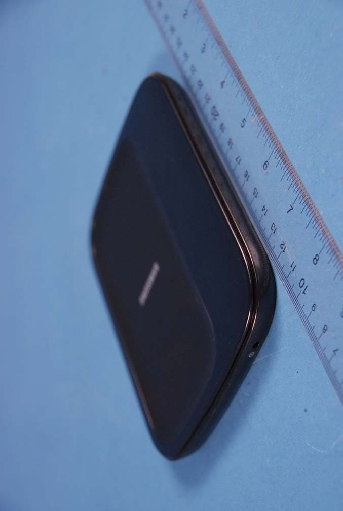
Click to zoom
Application Details
- Equipment Class
- DTS - Digital Transmission System
- Date of Grant
- May 30, 2012
- Application Purpose
- Original Equipment
- Date of Application
- May 21, 2012
- Equipment Note
- Wireless Charging Pad
- Frequency Range
- 2405.00000000 - 2470.00000000
- Company
- Samsung Electronics Co Ltd
- Country
- United States
Documents & Files
Document Text
Text extracted from the exhibit documents filed with the FCC. Open a document above to read the original.
Users Manual
Please read all Safety precautions before using your device to ensure safe and proper use. Samsung is not responsible for injuries or damages that result from improper usage or failure to follow safety precautions. Safety Precautions Do not use damaged power cords or plugs, or loose electrical sockets Do not touch the power cord with wet hands, or disconnect the charger by pulling on the cord Do not use damaged power cables and bend or damage power cables Do not use your device while charging or touch your device with wet hands Do not use your device close to metal objects such as coins, keys, or accessories Your device may overheat.• If you must use your device, keep it at least 30 cm away • from metal products. If the product overheats, remove the device from the product, disconnect the charger, and stop using the product for a while Prolonged exposure of your skin to an overheated device may cause low temperature burn symptoms, such as red spots and pigmentation. Do not store your device near or in heaters, microwaves, hot cooking equipment, or high pressure containers Your device may overheat and cause a fire. Do not drop your device or cause impacts to your device Do not store your device on slopes.• Your device may be damaged or parts may malfunction.• Do not allow your child or pet to suck or bite the device It may damage the device or cause a fire. Do not use the device for anything other than its intended use Keep your device dry place away from moisture or water Humidity and all types of liquids may damage device parts • or electronic circuits. If your device is wet, dry the device with a towel and take it • to a service centre. Do not disassemble, modify, or repair your device It may cause electrical shocks.• For service, take your device to a Samsung Service Centre.• Any changes or modifications to your device can void your • manufacturer’s warranty. Do not use your device near other electronic devices Most electronic devices use radio frequency signals. Your • device may interfere with other electronic devices. Do not use your device in a hospital or near medical • equipment that can be interfered with by radio frequency. If you personally use any medical equipment, contact the • manufacturer of the equipment to ensure the safety of your equipment from radio frequency. Graphics used in this manual are for illustration purposes. The actual products may vary. Unpack Charging Pad Charging CoverTravel Adapter Travel adapter appearance may vary depending on your region. Using the Wireless Charging System Connect the travel adapter to a mains outlet and plug 1 the charging jack into the Wireless charging pad. The buzzer will beep twice. If the buzzer doesn’t beep, disconnect and connect the travel adapter again. Replace your device’s the battery cover with the Wireless 2 charging cover, then place it on the Wireless charging pad to charge. The buzzer will beep and charging status indicators 3 are displayed on your device. When your device is fully charged, unplug the travel adapter from the wall outlet and the Wireless charging pad. The buzzer sounds when an abnormal situation • occurs while charging. Disconnect the travel adapter from the Wireless charging pad and stop using it for a while. Only use the provided pad and cover with the • dedicated mobile phone. Not compatible with WPC certified products. • Charging efficiency might be reduced if there’s an • object between the mobile device and the Wireless charging pad. 05/2012. Draft www.samsung.com Wireless Charging System Do not place the wireless charging cover separately on the wireless charging pad. The wireless charging cover will have electrical currents when positioned on the wireless charging pad. If the wireless charging cover is in contact with the wireless charging pad, it may cause a fire. FCC 1. Statement related Part15.21 Cautions Changes or modifications made in the device, not expressly approved by Samsung, will void the user’s authority to operate the equipment. The use of any unauthorized accessories may be dangerous and void the device warranty if said accessories cause damage or a defect to the device. Although your device is quite sturdy, it is a complex piece of equipment and can be broken. Avoid dropping, hitting, bending or sitting on it. 2. Statement related Part15.105 FCC Notice and Cautions This device complies with Part 15 of the FCC Rules. Operation is subject to the following two conditions: (1) this device may not cause harmful interference, and (2) this device must accept any interference received, including interference that may cause undesired operation. This equipment has been tested and found to comply with the limits for a Class B digital device, pursuant to part 15 of the FCC Rules. These limits are designed to provide reasonable protection against harmful interference in a residential installation. This equipment generates, uses and can radiate radio frequency energy and, if not installed and used in accordance with the instructions, may cause harmful interference to radio communications. However, there is no guarantee that interference will not occur in a particular installation. If this equipment does cause harmful interference to radio or television reception, which can be determined by turning the equipment off and on, the user is encouraged to try to correct the interference by one or more of the following measures: Reorient or relocate the receiving antenna.• Increase the separation between the equipment and • receiver. Connect the equipment into an outlet on a circuit • different from that to which the receiver is connected.• Consult the dealer or an experienced radio/TV • technician for help. The device may cause TV or radio interference if used in close proximity to receiving equipment. The FCC can require you to stop using the device if such interference cannot be eliminated. RFx information The RF field strength of the wireless device or devices that may be embedded in your devi…
Text truncated - open the document above for the full version.
Cover Letter(s)
SAMSUNG ELECTRONICS AMERICA, INC. American QA Lab 19 Chapin Rd, Building D. Pine Brook, NJ 07058 Date: May 18, 2012 Federal Communications Commission Authorization and Evaluation Division 7435 Oakland Mills Road, Columbia, MD 21046 RE: Request of Confidentiality for FCC ID: A3LEADS10EBE To Whom It May Concern: Pursuant to Sections 0.457 and 0.459 of the Commission’s Rules (CFR 47), and Section 552 (b) (4) of the Freedom of Information Act, SAMSUNG ELECTRONICS CO.,LTD. hereby requests confidentiality and treatment of certain information accompanying this application. The materials contain trade secrets and proprietary information not customarily released to the public. The public disclosure of these matters might be harmful to the Applicant and provide unjustified benefits to its competitors. We are also hereby request Short-Term Confidentiality for 180 days after the grant as outlined in Public Notice DA 04-1705. This provision will give SAMSUNG ELECTRONICS CO.,LTD. temporary confidentiality of commercially sensitive information prior to product release. The requested Permanent and Short-Term Confidential exhibits are listed as follows: PERMANENT AND SHORT-TERM CONFIDENTIAL LIST Exhibit Description 1 Block Diagram 2 Operational Description PERMANENT 3 Schematics 4 External Photos 5 Internal Photos 6 Test-Setup Photos SHORT-TERM 7 Users Manual The Applicant understands that pursuant to Rule 0.457, disclosure of this application and all accompanying documentations, where applicable, will not be made public before the date of the Grant for this application. Sincerely, Peter Ra General Manager American QA Lab SAMSUNG Electronics America INC.
External Photos
Samsung FCC ID: A3LEADS10EBE Model: EAD-S10EBE External Photos EUT Type: Wireless Charging Pad Page 1 of 4 © 2012 PCTEST Engineering Laboratory Inc. EXTERNAL PHOTOGRAPHS Samsung FCC ID: A3LEADS10EBE Model: EAD-S10EBE External Photos EUT Type: Wireless Charging Pad Page 2 of 4 © 2012 PCTEST Engineering Laboratory Inc. Samsung FCC ID: A3LEADS10EBE Model: EAD-S10EBE External Photos EUT Type: Wireless Charging Pad Page 3 of 4 © 2012 PCTEST Engineering Laboratory Inc. Samsung FCC ID: A3LEADS10EBE Model: EAD-S10EBE External Photos EUT Type: Wireless Charging Pad Page 4 of 4 © 2012 PCTEST Engineering Laboratory Inc.
ID Label/Location Info
Label and Location Samsung Model: EAD-S10EBE FCC ID: A3LEADS10EBE Label Location
Internal Photos
Samsung FCC ID: A3LEADS10EBE Model: EAD-S10EBE Internal Photos EUT Type: Wireless Charging Pad Page 1 of 5 © 2012 PCTEST Engineering Laboratory Inc. INTERNAL PHOTOGRAPHS Samsung FCC ID: A3LEADS10EBE Model: EAD-S10EBE Internal Photos EUT Type: Wireless Charging Pad Page 2 of 5 © 2012 PCTEST Engineering Laboratory Inc. Samsung FCC ID: A3LEADS10EBE Model: EAD-S10EBE Internal Photos EUT Type: Wireless Charging Pad Page 3 of 5 © 2012 PCTEST Engineering Laboratory Inc. Samsung FCC ID: A3LEADS10EBE Model: EAD-S10EBE Internal Photos EUT Type: Wireless Charging Pad Page 4 of 5 © 2012 PCTEST Engineering Laboratory Inc. Samsung FCC ID: A3LEADS10EBE Model: EAD-S10EBE Internal Photos EUT Type: Wireless Charging Pad Page 5 of 5 © 2012 PCTEST Engineering Laboratory Inc.
RF Exposure Info
Reviewed by: FCC ID: A3LEADS10EBE MAXIMUM PERMISSIBLE EXPOSURE (MPE) DATA REPORT Quality Manager Test Report S/N: Test Dates: EUT Type: 0Y1204200529.A3L May 2, 2012 Wireless Charging Pad Page 1 of 7 © 2012 PCTEST Engineering Laboratory, Inc. REV 3.1MPE 02/09/09 Applicant Name: Date of Testing: Samsung Electronics Co., Ltd. May 2, 2012 416 Maetan 3-Dong, Yeongtong-gu Test Site/Location: Suwon-si, Gyeonggi-do PCTEST Lab, Columbia, MD, USA 443-742 , Republic of Korea Test Report Serial No.: 0Y1204200529.A3L FCC ID: A3LEADS10EBE APPLICANT: Samsung Electronics Co., Ltd. EUT Type: Wireless Charging Pad FCC Rule Part(s): FCC Part 1 (§1.1310) and Part 2 (§2.1091) FCC Classification: Digital Transmission System (DTS) Test Procedure: OET Bulletin 65 The device bearing the FCC Identifier specified above has been shown to comply with the applicable technical standards as indicated in the measurement report and has been tested in accordance with the measurement procedures specified in FCC OET Bulletin 65 (See Test Report). These measurements were performed with no deviation from the standards. Test results reported herein relate only to the item(s) tested. I authorize and attest to the accuracy of data. All measurements reported herein were performed by me or were made under my supervision and are correct to the best of my knowledge and belief. I assume full responsibility for the completeness of these measurements and vouch for the qualifications of all persons taking them. PCTEST certifies that no party to this application has been subject to a denial of Federal benefits that include FCC benefits pursuant to Section 5301 of the Anti-Drug Abuse Act of 1988, 21 U.S.C. 862. PCTEST ENGINEERING LABORATORY, INC. 6660-B Dobbin Road, Columbia, MD 21045 USA Tel. 410.290.6652 / Fax 410.290.6554 http://www.pctestlab.com RF EXPOSURE EVALUATION (MAXIMUM PERMISSIBLE EXPOSURE) Reviewed by: FCC ID: A3LEADS10EBE MAXIMUM PERMISSIBLE EXPOSURE (MPE) DATA REPORT Quality Manager Test Report S/N: Test Dates: EUT Type: 0Y1204200529.A3L May 2, 2012 Wireless Charging Pad Page 2 of 7 © 2012 PCTEST Engineering Laboratory, Inc. REV 3.1MPE 02/09/09 TABLE OF CONTENTS 1.0 RF EXPOSURE EVALUATION – MAXIMUM PERMISSIBLE EXPOSURE (MPE) .........................3 1.1 INTRODUCTION ................................................................................................................................... 3 1.2 EUT DESCRIPTION .............................................................................................................................. 3 1.3 MPE REQUIREMENTS OVERVIEW..................................................................................................... 4 1.4 TEST EQUIPMENT ............................................................................................................................... 5 1.5 TEST CONFIGURATION AND DATA ................................................................................................... 5 2.0 CONCLUSION..................................................................................................................................7 Reviewed by: FCC ID: A3LEADS10EBE MAXIMUM PERMISSIBLE EXPOSURE (MPE) DATA REPORT Quality Manager Test Report S/N: Test Dates: EUT Type: 0Y1204200529.A3L May 2, 2012 Wireless Charging Pad Page 3 of 7 © 2012 PCTEST Engineering Laboratory, Inc. REV 3.1MPE 02/09/09 1.0 RF EXPOSURE EVALUATION – MAXIMUM PERMISSIBLE EXPOSURE (MPE) 1.1 Introduction This document is prepared on behalf of Samsung Electronics Co., Ltd. to show compliance with the RF Exposure requirements as required in §1.1310 of the FCC Rules and Regulations and RSS-102 of Industry Canada. The limit for Maximum Permissible Exposure (MPE), specified in FCC §1.1310, is listed in Table 1-1. According to FCC §1.1310 and RSS-102: the criteria listed in the following table shall be used to evaluate the environmental impact of human exposure to radio-frequency (RF) radiation as specified in §1.1307(b). Frequency Range (MHz) Electric Field Strength (V/m) Magnetic Field Strength (A/m) Power Density (mW/cm 2 ) Average Time (Minutes) (A) Limits For Occupational / Control Exposures (f = frequency) 30-300 61.4 0.163 1.0 6 300-1500 ... ... f/300 6 1500-100,000 ... ... 5.0 6 (B) Limits For General Population / Uncontrolled Exposure (f = frequency) 1.34–30 824/f 2.19/f *(180/f 2 ) 30 30-300 27.5 0.073 0.2 30 300-1500 ... ... f/1500 30 1500-100,000 ... ... 1.0 30 Table 1-1. Limits for Maximum Permissible Exposure (MPE) 1.2 EUT Description The Samsung Model: EAD-S10EBE is a wireless charging pad containing Zigbee and wireless charging circuit using ISM frequency of 6.78MHz. For this MPE evaluation the device is set to transmit and the RF exposure is evaluated. EUT: Model: EAD-S10EBE Grantee: Samsung Electronics Co., Ltd. FCC ID: A3LEADS10EBE Reviewed by: FCC ID: A3LEADS10EBE MAXIMUM PERMISSIBLE EXPOSURE (MPE) DATA REPORT Quality Manager Test Report S/N: Test Dates: EUT Type: 0Y1204200529.A3L May 2, 2012 Wireless Charging Pad Page 4 of 7 © 2012 PCTEST Engineering Laboratory, Inc. REV 3.1MPE 02/09/09 1.3 MPE Requirements Overview Three different categories of transmitters are defined by the FCC in OET Bulletin 65. These categories are fixed installation, mobile, and portable and are defined as follows: o Fixed Installations: fixed location means that the device, including its antenna, is physically secured at a permanent location and is not able to be easily moved to another location. Additionally, distance to humans from the antenna is maintained to at least 2 meters. o Mobile Devices: a mobile device is defined as a transmitting device designed to be used in other than fixed locations and to be generally used in such a way that a separation distance of at least 20 centimeters is normally maintained between the transmitter's radiating structures and the body of the user or nearby persons. Transmitters designed to be used by consumers or workers that can be easily re-located, such as a wireless…
Text truncated - open the document above for the full version.
Test Report
Reviewed by: FCC ID: A3LEADS10EBE FCC Pt. 15.247 802.15.4 ZIGBEE TEST REPORT (CERTIFICATION) Quality Manager Test Report S/N: Test Dates: EUT Type: 0Y1204200528.A3L March 26 - April 26, 2012 Wireless Charging Pad Page 1 of 34 © 2012 PCTEST Engineering Laboratory, Inc. REV 2.8WBG 11/18/2009 Applicant Name: Date of Testing: Samsung Electronics, Co. Ltd. March 26 - April 26, 2012 416 Maetan 3-Dong, Yeongtong-gu Test Site/Location: Suwon-si, Gyeonggi-do PCTEST Lab, Columbia, MD, USA 443-742 , Republic of Korea Test Report Serial No.: 0Y1204200528.A3L FCC ID: A3LEADS10EBE APPLICANT: Samsung Electronics, Co. Ltd. Application Type: Certification Model(s): EAD-S10EBE EUT Type: Wireless Charging Pad Max. RF Output Power: 2.932 mW (4.671 dBm) Peak Conducted Frequency Range: 2405 - 2470 MHz FCC Classification: Digital Transmission System (DTS) FCC Rule Part(s): Part 15.247 This equipment has been shown to be capable of compliance with the applicable technical standards as indicated in the measurement report and was tested in accordance with the measurement procedures specified in ANSI C-63.4-2003. Test results reported herein relate only to the item(s) tested. I attest to the accuracy of data. All measurements reported herein were performed by me or were made under my supervision and are correct to the best of my knowledge and belief. I assume full responsibility for the completeness of these measurements and vouch for the qualifications of all persons taking them. PCTEST certifies that no party to this application has been subject to a denial of Federal benefits that includes FCC benefits pursuant to Section 5301 of the Anti-Drug Abuse Act of 1988, 21 U.S.C. 862. PCTEST ENGINEERING LABORATORY, INC. 7185 Oakland Mills Road, Columbia, MD 21046 USA Tel. 410.290.6652 / Fax 410.290.6554 http://www.pctestlab.com MEASUREMENT REPORT FCC PART 15.247 WPAN 802.15.4 Zigbee Reviewed by: FCC ID: A3LEADS10EBE FCC Pt. 15.247 802.15.4 ZIGBEE TEST REPORT (CERTIFICATION) Quality Manager Test Report S/N: Test Dates: EUT Type: 0Y1204200528.A3L March 26 - April 26, 2012 Wireless Charging Pad Page 2 of 34 © 2012 PCTEST Engineering Laboratory, Inc. REV 2.8WBG 11/18/2009 TABLE OF CONTENTS FCC PART 15.247 MEASUREMENT REPORT...................................................................................3 1.0 INTRODUCTION......................................................................................................................................4 1.1 SCOPE....................................................................................................................................................... 4 1.2 PCTEST TEST LOCATION........................................................................................................................ 4 2.0 PRODUCT INFORMATION .....................................................................................................................5 2.1 EQUIPMENT DESCRIPTION..................................................................................................................... 5 2.2 EUT CAPABILITIES ................................................................................................................................... 5 2.3 EMI SUPPRESSION DEVICE(S)/MODIFICATIONS.................................................................................. 5 2.4 LABELING REQUIREMENTS .................................................................................................................... 5 3.0 DESCRIPTION OF TEST ........................................................................................................................6 3.1 EVALUATION PROCEDURE..................................................................................................................... 6 3.2 AC LINE CONDUCTED EMISSIONS......................................................................................................... 6 3.3 RADIATED EMISSIONS ............................................................................................................................ 7 4.0 ANTENNA REQUIREMENTS ..................................................................................................................8 5.0 TEST EQUIPMENT CALIBRATION DATA..............................................................................................9 6.0 TEST RESULTS ....................................................................................................................................10 6.1 SUMMARY ............................................................................................................................................... 10 6.2 6DB BANDWIDTH MEASUREMENT .......................................................................................................11 6.3 OUTPUT POWER MEASUREMENT .......................................................................................................14 6.4 POWER SPECTRAL DENSITY ............................................................................................................... 15 6.5 CONDUCTED EMISSIONS AT THE BAND EDGE.................................................................................. 18 6.6 CONDUCTED SPURIOUS EMISSIONS .................................................................................................. 20 6.7 RADIATED SPURIOUS EMISSION MEASUREMENTS.......................................................................... 25 6.8 RADIATED RESTRICTED BAND EDGE MEASUREMENTS .................................................................. 30 6.9 LINE-CONDUCTED TEST DATA............................................................................................................. 32 7.0 CONCLUSION .......................................................................................................................................34 Reviewed by: FCC ID: A3LEADS10EBE FCC Pt. 15.247 802.15.4 ZIGBEE TEST REPORT (CERTIFICATION) Quality Manager Test Report S/N: Test Dates: EUT …
Text truncated - open the document above for the full version.
Test Setup Photos
Samsung FCC ID: A3LEADS10EBE Model: EAD-S10EBE Test Set-Up Photos EUT Type: Wireless Charging Pad Page 1 of 3 © 2012 PCTEST Engineering Laboratory Inc. TEST SETUP PHOTOGRAPHS Figure 1 Line Conducted Test Setup Figure 2 Line Conducted Test Setup Samsung FCC ID: A3LEADS10EBE Model: EAD-S10EBE Test Set-Up Photos EUT Type: Wireless Charging Pad Page 2 of 3 © 2012 PCTEST Engineering Laboratory Inc. Figure 3 Radiated Test Setup Figure 4 Radiated Test Setup Samsung FCC ID: A3LEADS10EBE Model: EAD-S10EBE Test Set-Up Photos EUT Type: Wireless Charging Pad Page 3 of 3 © 2012 PCTEST Engineering Laboratory Inc. Figure 5 Radiated Test Setup Figure 6 Radiated Test Setup
Contact Information
Applicant
Jenni Chun(General Manager)
Technical Contact
PCTEST Engineering Lab., Inc.Randy Ortanez
[email protected]410-290-6652
6660-B Dobbin Road · Columbia, Maryland · United States
Test Firm
PCTEST Engineering Laboratory, Inc.Randy Ortanez
Technical Specifications
| # | Rule Parts | Frequency Range | Power Output |
|---|---|---|---|
| 1 | 15C | 2.40 GHz - 2.47 GHz | 3.00 mW |
Other Applications from Samsung Electronics Co Ltd
A3LSMS741B
Aug 05, 2026Portable Handset
Equipment Class
6VL - 15E 6 GHZ Very Low Power DeviceA3LSMX940
Jul 31, 2026BT,BLE Tablet DTS,UNII a,b,g,n,ac,ax,be and digitizer
Equipment Class
DTS - Digital Transmission SystemA3LSMS741U
Jul 30, 2026Portable Handset
Equipment Class
6CD - 15E 6 GHz Low Power Dual ClientA3LSMX840
Jul 27, 2026BT,BLE Tablet DTS,UNII a,b,g,n,ac,ax and Digitizer
Equipment Class
DSS - Part 15 Spread Spectrum TransmitterA3LSMX848U
Jul 27, 2026WCDMA, LTE, 5G NR Tablet BT,BLE, DTS,UNII a b g n ac ax and Digitizer
Equipment Class
JBP - Part 15 Class B Computing Device Peripheral