A72-BTX330MOBILE PHONE - BLUETOOTH PORTION
AEG Telecomunicacoes, S.A.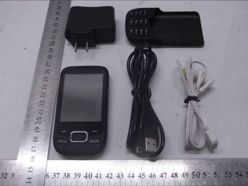
Click to zoom
Application Details
- Equipment Class
- DXX - Part 15 Low Power Communication Device Transmitter
- Date of Grant
- Dec 27, 2011
- Application Purpose
- Original Equipment
- Date of Application
- Dec 27, 2011
- Equipment Note
- MOBILE PHONE - BLUETOOTH PORTION
- Frequency Range
- 2402.00000000 - 2480.00000000
- Company
- AEG Telecomunicacoes, S.A.
- Country
- Portugal
Documents & Files
Document Text
Text extracted from the exhibit documents filed with the FCC. Open a document above to read the original.
Users Manual
BTX330 User Manual - 0 - Table of Contents 1 SAFETY AND GENERAL INFORMATION................................................................................................................. 1 1.1 BRIEFINTRODUCTION................................................................................................................................................... 1 1.2 I MPORTANTSAFETYPRECAUTIONS................................................................................................................................. 1 1.2.1 General Precautions........................................................................................................................................ 1 1.2.2 Phone Precautions........................................................................................................................................... 1 1.2.3 Battery Safety Precautions............................................................................................................................. 2 1.2.4 Disposing of Used Battery.............................................................................................................................. 2 1.2.5 Charger Precautions........................................................................................................................................ 3 1.2.6 Clean and Maintenance.................................................................................................................................. 3 1.3 T ERMINOLOGY EXPLANATION......................................................................................................................................... 3 2 SPECIFICATION............................................................................................................................................................. 4 2.1 S PECIFICATION.............................................................................................................................................................. 4 2.2 T ECHNICALPERFORMANCE............................................................................................................................................. 4 3 PHONE APPEARANCE AND KEYS..............................................................................................................................5 3.1 P HYSICALIMPRESSION.................................................................................................................................................. 5 3.2 K EYS SPECIFICATION..................................................................................................................................................... 5 3.3 I CONS........................................................................................................................................................................... 6 4MENUFUNCTION........................................................................................................................................................... 6 5USERGUIDE.................................................................................................................................................................... 7 5.1 I NSTALLING/REMOVING THE BATTERY........................................................................................................................... 7 5.2 C HARGING THE BATTERY................................................................................................................................................ 8 5.3 INSERTING/REMOVING THESIMCARD.......................................................................................................................... 8 5.4 T-FLASH CARD USE....................................................................................................................................................... 8 5.4.1 Installing/Removing T-Flash card.................................................................................................................. 8 5.4.2 T-Flash card use.............................................................................................................................................. 9 5.5 P OWERONOROFF...................................................................................................................................................... 9 6CALLFUNCTIONS.......................................................................................................................................................... 9 6.1 M AKING ACALL............................................................................................................................................................ 9 6.2 A NSWERING ACALL.................................................................................................................................................... 10 6.3 H-F REE/H-HELD......................................................................................................................................................... 10 6.4 CALLWAITING............................................................................................................................................................ 10 6.5 C ALLOPTIONS............................................................................................................................................................ 10 6.5.1 During a call................................................................................................................................................... 10 6.5.2 Making a Multiparty Call............................................................................................................................... 10 7PHONEBOOK.................................................................................................................................................................11 7.1 A DD NEW CONTACT.................................................…
Text truncated - open the document above for the full version.
Cover Letter(s)
AEG Telecomunicações, S.A. FCC ID: A72-BTX330 POWER OF ATTORNEY December 19, 2011 Federal Communications Commission Authorization and Evaluation Division 7435 Oakland Mills Road Columbia, MD 21046 To Whom It May Concern: We, AEG Telecomunicações, S.A., hereby authorize MOSTTechnology Service Co., Ltd.(Terry YANG/ Manager) on our behalf, to apply to the Federal Communications Commission on our equipment. Any and all acts carried out byMOST Technology Service Co., Ltd.(Terry YANG/ Manager) on our behalf shall have the same effect as acts of our own. This authorization expires onJanuary 31, 2012. This is to advise that we are in full compliance with the Anti-Drug Abuse Act. We, IVIO INTERNATIONAL LTD are not subject to a denial of federal benefits pursuant to Section 5301 of the Anti-Drug Act of 1988, 21 USC853a, and no party to the application is subject to a denial of federal benefits pursuant to that section. Sam Li Director AEG Telecomunicações, S.A. December 19, 2011
External Photos
FCC ID: A72-BTX330 Report No.: STS111104F1 FRONT VIEW OF SAMPLE FCC ID: A72-BTX330 Report No.: STS111104F1 BACK VIEW OF SAMPLE FCC ID: A72-BTX330 Report No.: STS111104F1 LEFT VIEW OF SAMPLE RIGHT VIEW OF SAMPLE FCC ID: A72-BTX330 Report No.: STS111104F1 TOP VIEW OF SAMPLE BOTTOM VIEW OF SAMPLE FCC ID: A72-BTX330 Report No.: STS111104F1 PHOTO OF POWER SUPPLY PHOTO OF HEADPHONE FCC ID: A72-BTX330 Report No.: STS111104F1Page 39 of 47 PHOTO OF USB PHOTO OF BATTERY FCC ID: A72-BTX330 Report No.: STS111104F1 PHOTO OF THE ENTIRE SAMPLE
Internal Photos
FCC ID: A72-BTX330 Report No.: STS111104F INTERNAL PHOTO OF SAMPLE – 1 INTERNAL PHOTO OF SAMPLE – 2 FCC ID: A72-BTX330 Report No.: STS111104F1 INTERNAL PHOTO OF SAMPLE –3 INTERNAL PHOTO OF SAMPLE –4 FCC ID: A72-BTX330 Report No.: STS111104F1 INTERNAL PHOTO OF SAMPLE –5 INTERNAL PHOTO OF SAMPLE –6 FCC ID: A72-BTX330 Report No.: STS111104F1 INTERNAL PHOTO OF SAMPLE –7 INTERNAL PHOTO OF SAMPLE –8 FCC ID: A72-BTX330 Report No.: STS111104F1 INTERNAL PHOTO OF SAMPLE–9 INTERNAL PHOTO OF SAMPLE –10 FCC ID: A72-BTX330 Report No.: STS111104F1 INTERNAL PHOTO OF SAMPLE –11 INTERNAL PHOTO OF POWER SUPPLY-1 FCC ID: A72-BTX330 Report No.: STS111104F1 INTERNAL PHOTO OF POWER SUPPLY-2
Operational Description
1/2 Operation Description OPERATIONAL DESCRIPTION APPLICANT:AEGTelecomunicações,S.A. Manufacturer: HongKongSharpTechnologyLimited FCC ID: A72-BTX330 Instruction Book: Users Manual Frequency Range GSM Transmit Frequency Band: 824.2-848.8 MHz Receive Frequency Band: 849.2-893.8 MHz Transmit Frequency Band: 1850.2-1909.8 MHz Receive Frequency Band: 1930.2-1989.8 MHz Specific Operating Power Range: Power Class 1; Power Control Level 0 +30dBm +2.0dB/-2.0dB Power Control Level 1 +28dBm +3.0dB/-3.0dB Power Control Level 2 +26dBm +3.0dB/-3.0dB Power Control Level 3 +24dBm +3.0dB/-3.0dB Power Control Level 4 +22dBm +3.0dB/-3.0dB Power Control Level 5 +20dBm +3.0dB/-3.0dB Power Control Level 6 +18dBm +3.0dB/-3.0dB Power Control Level 7 +16dBm +3.0dB/-3.0dB Power Control Level 8 +14dBm +3.0dB/-3.0dB Power Control Level 9 +12dBm +4.0dB/-4.0dB Power Control Level 10 +10dBm +4.0dB/-4.0dB Power Control Level 11 +8dBm +4.0dB/-4.0dB Power Control Level 12 +6dBm +4.0dB/-4.0dB Power Control Level 13 +4dBm +4.0dB/-4.0dB Power Control Level 14 +2dBm +5.0dB/-5.0dB Power Control Level 15 +0dBm +5.0dB/-5.0dB Note; Effective radiation efficiency is –3.7dB DC Voltage and Current into the Final Amplifier Module: Supply Voltage = 5.0Vdc Supply Current = ~0.5Amp. Tune-up Procedure: Tune-up Procedure Equipment Identification: Equipment's Identification label and its intended Location are as shown in EXHIBIT Type “ID Label / Location Information” (FCC ID Nameplate), and in EXHIBIT Type “Internal Photo”(Photograph of inside) Photographs: A complete set of the Photographs showing External and Internal Views of Circuit Details and Construction are provided by from EXHIBIT Type “External Photos” and “Internal Photos”. Accessories: Accessories 2/2 Operation Description Figure 1.2: Terminal Components (Accessories) Technical Descriptions TX synthesizer uses an Offset-PLL circuit. The Offset-PLL circuit consists of PLL-IC and TX_VCO and loop filter. Reference frequency of the above synthesizers is 26MHz and generated by VCTCXO. Control signal is sent from Baseband section and keeps frequency stability. TX IQ signal is input from Baseband section to MT6235, The Bluetooth signal is input form MT6601 and FM signal is input form TLG1120 section to MT6235. TX IQ signal is applied to the quadrature up-converter, and the up-converter LO signal is generated from the transceiver VCO within MT6139B. This up-converter translates the GMSK-modulated signal to an intermediate frequency (IF) that forms one input to a frequency/phase detector circuit. This IF signal is the reference input to an Offset-PLL circuit. The feedback path of this Offset-PLL circuit includes a down-conversion from the RF output frequency range to the IF range. The two inputs to this down-conversion mixer are formed the TX_VCO output and the LO generation circuits. The mixer output is the offset feedback signal that forms the variable input to a frequency/phase detector circuit. The detector compares its variable input to its reference input and generates an error signal that is low-pass filtered by the loop filter and applied to TX_VCO to force the RF frequency in the direction that minimizes errors. The TX_VCO output passes PA, Antenna SW, Coaxial connector with switch and emitted from embedded antenna. Digital Modulation: Analog speech produced by a microphone is encoded to digital PCM samples using a CODEC. The PCM samples are passed to a Vocoder for AMR (Advanced Multi Rate) encoding, to compress the speech samples. The encoding rate is determined by the Vocoder which formats the speech samples as data packets. A new data packet with data rate information is read by the microprocessor every 20 ms. The speech CODEC becomes AMR, FR(Full Rate), EFR(Enhanced FR) and HR(Half Rate). The microprocessor then sends the data packet to the transmit subsystem, and passed DAC to covert analog signal. I/Q base band signal is filtered and is inputted into 6M4003 containing quadrature phase modulator. Battery AC Charger
Parts List/Tune Up Info
版本 序 名称规格型号品牌商单位 位号单套备注 1 MTK基带芯片MT6253ANMTK pcs U1011 2TX Module2频RF7170D RFMD pcs U6011 3FlashSamsung ULPC 113MHz ADMUX K5N2866ATF—BQ12 SAMSUNGpcs U4011 4充电MOSFETWDFN-6L 2x2RP1800ACQWRICHPOWERpcs U2021 5音频功放D类PAM8303CAZNPAMpcs U3041 6 MOSFET_NEMT32SK3019ROHMpcs Q5031 7 26M晶体FOR MT6253(负载电容7.5PF) 7M26000028 TZ1689A X1E000021043400 TXC TST EPSON pcs U6021 8压敏电阻 SFI0402-120E100NP-LF MLVG0402100NV18BP HL0402-120E100NP-LF SFI 佳邦科技 HYLINK pcs T3 T301 T302 T308 T309 T312 T313 T501 T502 T505 T506 T507 T510 T511 T512 T513 T514 T705 T706 T707 T708 T709 T710 T711 T712 T714 T715 T723 T724 T7222 30 9 32KHZ晶体 32k crystal (32.768kHz,7pF ±20ppm) MS2V-T1S SSP-T7 Q13MC1461000200 MICRO CRYSTAL SIT e pson pcs X2011 10FPC连接器8PIN正压连接器BAT-1208X-04E广亚讯pcs CON1 CON22 11SIM卡座1.5高带桥带档16.4*16.3 CAF99-06153-1503LCN pcs J701 J7022 12T卡座掀盖卡座,高度1.6CAF11-08163-SF00 LCN pcs J7031 13系统连接器7PIN破板 IOUAF95-07164-0311LCNpcs J5031 14电池连接器4.2H 3.7P刀片电池座PAN37-03423-1002 LCN pcs BT4001 154pin TP连接器4pin TP连接器BL115-04RL-TAGF日慎pcs J5041 16G网BB屏蔽罩Z16_SC_GBB_V1迪顺鑫pcs 1 18 射频测试座 MHC-310 C90-101-0004 2RF1500-000111 Amphenol SpeedTech 信音电子 pcsJ6001 19 陶瓷电容CAP,1.5pF±0.25pF,50V,0402 GRM1555C1H1R5CZ01D C1005C0G1H1R5DT GRM1555C1H1R5CZ01D TaiyoYuden TDK MURATA pcs C669,C6702 20 陶瓷电容CAP,1.2pF±5%,50V,0402 GRM1555C1H1R2CZ01D C1005C0G1H1R2DT GRM1555C1H1R2CZ01D MURATA TAIYOYUDEN TDK pcs C601,C6022 21 陶瓷电容CAP,2pF±0.5pF,50V,0402 GRM1555C1H2R0CZ01D C1005C0G1H260DT GRM1555C1H2R0CZ01D TaiyoYuden TDK MURATA pcs C671,C672,C673,C6744 22 陶瓷电容CAP,3.9pF±5%,50V,0402 GRM1555C1H3R9CZ01D C1005C0G1H3R9DT GRM1555C1H3R9CZ01D MURATA TAIYOYUDEN TDK pcs C667,C6682 23 陶瓷电容CAP,12pF±5%,50V,0402 GRM1555C1H12R0CZ01D C1005C0G1H120DT GRM1555C1H12R0CZ01D MURATA TAIYOYUDEN TDK pcs C209,C2102 24 陶瓷电容CAP,5.6pF±0.5pF,50V,0402 GRM1555C1H5R6CZ01D C1005C0G1H5R6DT GRM1555C1H5R6CZ01D TaiyoYuden TDK MURATA pcs C6151 25 陶瓷电容CAP,6pF±0.5pF,50V,0402 GRM1555C1H6R0CZ01D C1005C0G1H060DT GRM1555C1H6R0CZ01D TaiyoYuden TDK MURATA pcs C6501 26 陶瓷电容CAP,22pF±5%,50V,0402 UMK105CH220JW-F C1005C0G1H220JT GRM1555C1H220JZ01D TaiyoYuden TDK MURATA pcs C639,C640,C646,C649,C651,C711,C7127 27 陶瓷电容CAP,33pF±5%,50V,0402 UMK105CG330JW-F C1005C0G1H330JT GRM1555C1H330JZ01D TaiyoYuden TDK MURATA pcs C308,C309,C313,C314,C315,C328,C330,C331 ,C333,C643,C644,C305,C319 13 28 陶瓷电容CAP,56pF±5%,50V,0402 UMK105CG560JW-F C1005C0G1H560JT GRM1555C1H560JZ01D TaiyoYuden TDK MURATA pcs C6471 29 陶瓷电容CAP,220pF±5%,50V,0402 UMK105CG221JW-F C1005C0G1H221JT GRM1555C1H221JD01D TaiyoYuden TDK MURATA pcs C6481 30 陶瓷电容CAP,100nF±10%,10V,X5R,0402 LMK105BJ104KV-F C1005X5R1A104KT GRM155R61A104KA01D TaiyoYuden TDK MURATA pcs C203,C204,C205,C206,C207,C303,C304,C310 ,C311,C339,C345,C342,C621,C624,C652 15 31陶瓷电容CAP,100pF±5%,50V,0402 UMK105CG101JW-F C1005C0G1H101JT GRM1555C1H101 JD01D TaiyoYuden TDK MURATA pcs C301,C312,C329,C332,C7105 32 陶瓷电容CAP,1nF±10%,16V,X7R,0402 UMK105BJ102KV-F C1005X7R1H102KT GRM155R71H102KA01D TaiyoYuden TDK MURATA pcs C637,C356,C3573 33 陶瓷电容CAP,1uF±10%,6.3V,X5R,0402 JMK105BJ105KV-T C1005X5R0J105KT GRM155R60J105KE19D TaiyoYuden TDK MURATA pcs C101,C102,C201,C208,C211,C212,C214,C216 ,C217,C218,C220,C221,C222,C223,C224,C22 5,C226,C227,C616,C620,C733 21 34 陶瓷电容 CAP,4.7uF± 10%,6.3V,X5R,0603 JMK107BJ475KV-T C1608X5R0J475KT GRM188R60J475KE19D TaiyoYuden TDK MURATA pcs C202,C213,C215,C219,C228,C229,C231,C302 ,C338,C511,C513,C552 12 35 陶瓷电容 CAP,2.2uF± 10%,6.3V,X5R,0603 JMK107BJ225KV-T C1608X5R0J225KT GRM188R60J225KE01D TaiyoYuden TDK MURATA pcs C401,C512,C703,C7044 36 陶瓷电容CAP,22uF±20%,6.3V,X5R,0805 CM21X5R226M06AT C2012X5R0J226MT TaiyoYuden TDK pcs C232,C653,C6543 37陶瓷电容 CAP,10uF±10%,6.3V,X5R,0805 高度0.85MM CM21X5R106K06AT C2012X5R0J106KT TaiyoYuden TDK MURATA 只 C306,C3072 38 贴片电阻0R(0402-0.0625W-J) MCR01MZSJ000 RC0402JR-070RL ROHM YAGEO pcs R208,R209,R221,R601,R607,R612,R616,,L60 1,R508 9 39 贴片电阻0.39R (1% 0805 1/4W)MCR10EZHFLR39ROHMpcs R2021 40 贴片电阻100R(0402-0.0625W-J) MCR01MZSJ101 RC0402JR-07100RL ROHM YAGEO pcsR304,R3052 41贴片电阻51R(0402-51R-0.0625W-J)MCR01MZSJ510ROHMpcs R505,R6082 42 贴片电阻1K(0402-0.0625W-J) MCR01MZSJ102 RC0402JR-071KL ROHM YAGEO pcs R204,R205,R303,R308,R506,R507,R610,R611 ,R613,R302,R310 11 43 贴片电阻1.5K(0402-0.0625W-J) MCR01MZSJ152 RC0402JR-071K5L ROHM YAGEO pcs R301,R3112 44 贴片电阻10R(0402-0.0625W-J) MCR01MZSJ100 RC0402JR-0710RL ROHM YAGEO pcsR703,R7082 45 贴片电阻2.0K(0402-0.0625W-J) MCR01MZSJ202 RC0402JR-072KL ROHM YAGEO pcsR306,R3072 46 贴片电阻4.7K(0402-0.0625W-J) MCR01MZSJ472 RC0402JR-074K7L ROHM YAGEO pcs R511,R5122 47 贴片电阻5.1K(0402-0.0625W-J) MCR01MZSJ512 RC0402JR-075K1L ROHM YAGEO pcs R1011 48 贴片电阻10K(0402-0.0625W-J) MCR01MZSJ103 RC0402JR-0710KL ROHM YAGEO pcs R102,R201,R309 R614,R5015 49 贴片电阻24K(0402-0.0625W-J) MCR01MZSJ243 RC0402JR-0724KL ROHM YAGEO pcs R6151 50 贴片电阻47K(0402-0.0625W-J) MCR01MZSJ473 RC0402JR-0747KL ROHM YAGEO pcs R336,R3342 51 叠层电感0402-47nH MLK1005S47NJT HK100547NJ-T SDCL1005C47N JT Murata CTC 顺络 pcsL5111 52滤波器 1800/1900SFWG42MY002WISOL pcs Z6021 53滤波器 850/900SFWM81DY102WISOL pcs Z6011 54 贴片电阻100K(0402-0.0625W-J) MCR01MZSJ104 RC0402JR-07100KL ROHM YAGEO pcs R1051 55叠层电感0402-2.7nH LQG15HN2N7S02Murata pcsC6621 56叠层电感0402-3.3nH LQG15HN3N3S02Murata pcsC6591 57叠层电感0402-3.9nH LQG15HN3N9S02Murata pcsL6171 58叠层电感0402-4.3nHLQG15HN4N3S02MuratapcsL612,L6142 59叠层电感0402-18nH LQG15HN18NJ02Murata pcsL608,L6102 60 磁珠600@1GHZ,0402HFJ100505T-601Y-NCHILISINpcsB101,B102,B304,B305 4 61 功率电感IND,4.7uH±10%,0805 LD0805-4R7K-N MGFL2012F4R7MT chilisin Micro gate pcs L201,L2022 62 磁珠1800@1GHz,0402,HFJ100505T-182Y-NCHILISINpcsB301,B306,B501,B502,B503 5 63 磁珠75@100MHZ,0402 BLM15BB750SN1 BK1005LL750-T SZ1005G750 Murata TaiyoYuden 顺络 pcsB6011 64 磁珠180@100MHZ,0603 FBMH1608HM181-T MPZ1608S181A SZ1608G181 TaiyoYuden TDK 顺络 pcsB201,B202,B205,B302,B3035 65 磁珠1000@100MHZ,0603,耐流800mAPBY160808T-102Y-NCHILISINpcs B506 B3072 66 齐纳二极管 SOD-523 封装 5.1V,500mAPZ5D4V2HPrisemipcsD2011 67 PCBZ16-V3.0pcs 1 68 蓝牙芯片QFN-40MT6622MTKpcs U9011 69BT-SAW RFBPF1608070A09FNH LFB182G45SG9A293_CA293- STD-A BF1608-L2R4DAAT /LF Walsin Murata ACX 美磊 pcs U9021 71陶瓷…
Text truncated - open the document above for the full version.
Parts List/Tune Up Info
Tune-Up Procedure A--Tune-Up TX 1 Purpose This panel gives the possibility to manage the mobile in the transmit mode. This window includes both: - all the parameters (frequency band, RF channel, RF level to get the desire antenna output power...) the user needs to make the mobile transmitting, - all the parameters needed to define a transmit burst, - all the compensation table to be able to align the mobile in production. This Tx command user guide is describing: - the characteristics of the transmit burst, - all the parameters used in the transmit mode, - the operating mode to make the mobile transmitting 2 General description 2.1 Characteristics of the transmit burst The power levels and the shape of a transmit burst are controlled by the power amplifier controller RF7170TR. The burst is generated by a 10-bits DAC from the RF7170TR as shown below: The ramping shape is referenced with the rising edge of Tx-ON (from the Baseband). There are two types of parameters define the transmit burst: the first one define the shapes of the burst, and the second one define the temporal position of the burst. The rising and the falling edge of the transmit burst are determined by a set of 32 DAC code values n = 0 ... 31. Tru = TxTRUDefault + △TRU_P + △TRU_T Trd = TxTRD_NBDefault + △TRD_P (for a normal burst). Trd = TxTRD_ABDefault + △TRD_P (for an access burst). 3 Parameters F(n) are values coming from the DAC to shape the transmit burst. Some F(n) values have a corresponding parameter used in the TAT to align the mobiles. Parameter used in TAT = [F(n)]. 3.1 Parameters used to shape the burst - H0 = [F(1)] controls the rate at which energy is given to the control loop at the beginning of the ramp. This energy is needed to bring the PA system control in a closed loop. - PeakPow = [F(15)] corresponds to the peak power of the transmit burst. - H30 = [F(30)] corresponds to the last ramping coefficients used to shape the ramp. - MinPow = [F(31)] is a fixed parameter and corresponds to the Code Start of the SI4220 specification. It ensures a fast discharge of accumulated energy during the open loop mode in the summing node. 3.2 Parameters used to define the temporal position of the burst 3.2.1 Optimum position of the burst This parameter is TRU (or △TRU_P) on the panel, in the Optimal Burst. This is the burst starting time correction, which is optimised for each power control level. (Note that _P means that the parameter is a power compensation parameter). 3.2.2 Optimum length of the burst This parameter is TRD (or △TRD_P) on the panel, in the Optimal Burst. This is the burst length compensation, which is optimised for each power control level. (Note that _P means that the parameter is a power compensation parameter). 4 Operating mode 4.1 How to transmit a Tch burst (Random data), 4.1.1 In GSM850 mode, channel 190, at power control level max Connect the mobile with special software, Configuration of the common parameters: - Band: GSM850, - Channel: 190, - RF level: 5, - Burst select: Mode Tch Random Press STAR command to start continuous TX, you can check the burst with CMU200 or Agilent 8960, it must fit the curve below. 4.1.2 How to transmit a Tch burst (Random data), 4.1.3 In GSM900 mode, channel 124, at power control level max Connect the mobile with special software, Configuration of the common parameters: - Band: GSM900, - Channel: 124, - RF level: 5, - Burst select: Mode Tch Random Press STAR command to start continuous TX, you can check the burst with CMU200 or Agilent 8960, it must fit the curve below. The request of the Power vs Time. 4.1.2 In PCS1900 mode, channel 661, at power control level max: Connect the mobile with special software, Configuration of the common parameters: - Band: PCS1900 - Channel: 661, - RF level: 0, - Burst select: Mode Tch Random Press STAR command to start continuous TX, you can check the burst with CMU200 or Agilent 8960, it must fit the curve below. In DCS1800 mode, channel 885, at power control level max: Connect the mobile with special software, Configuration of the common parameters: - Band:DCS1800 - Channel: 885, - RF level: 0, - Burst select: Mode Tch Random Press STAR command to start continuous TX, you can check the burst with CMU200 or Agilent 8960, it must fit the curve below. 4.2 How to stop Tx measurements: Press STOP command to stop the TX.. 4.3 How to transmit a burst after modifying parameters. Please note that each time a parameter (such as parameter used to shape the burst) is changed, then the user has to download to flash to validate the parameter modification. If the command is not performed, the old parameters are taken into account B--Tune-Up Frequency 5 Purpose This panel gives the description of the Frequency plan. This window includes both: - Automatic frequency control(AFC), - Static frequency error and range, - Dynamic frequency error and range 6 Automatic frequency control Before a handset is allowed to transmit any signals, it needs to first receive the FSB signal from the base station, demodulate and decode it using its own local oscillator, map it to the constellation plane, calculate the frequency offset, and adjust the local oscillator accordingly, until 0.1ppm of frequency accuracy is achieved. This frequency correction loop is called the automatic frequency control (AFC) loop in GSM standard. The process as below: In MT6223, it uses a AFC signal from baseband (DAC) to finish automatic frequency control. 7 Static frequency error and range ● Factors of static frequency error: manufacturing frequency tolerance in crystal at room temperature, aging, ● Static frequency error is compensated for using 6bits programming capacitor array (CAP ID). ● The static frequency range of capacitor array( CAP ID=0 to63) must larger than 34ppm( +-17ppm). ● The static range depends on crystal ‘s TS and CL ● The capacitor array calibration is done in production testing by setting the AFC DAC to mid-scale(4196) and adjusting CAP ID to the setting that give c…
Text truncated - open the document above for the full version.
Test Report
FCC 47 CFR PART 15 SUBPART C TEST REPORT For Applicant: AEG Telecomunicações, S.A. Address: Rua João Saraiva, 4, 1700-249 Lisboa, Portugal Product Name: Mobile Phone Model Name: BTX330 Brand Name: AEG FCC ID: A72-BTX330 Report No.: STS111104F2 Date of Issue: December. 15, 2011 Issued by: MOST Technology Service Co., Ltd. Address: No.5, 2nd Langshan Road, North District, Hi-tech Industrial Park, Nanshan, Shenzhen, Guangdong, China Tel: 86-755-2795 8522 Fax: 86-755-2795 8022 The report consists 43 pages in total. It may be duplicated completely for legal use with the approval of the applicant. It should not be reproduced except in full, without the written approval of our laboratory. The client should not use it to claim product endorsement by MOST. The test results in the report only apply to the tested sample. The test report shall be invalid without all thesignatures of testing engineers, reviewer and approver. FCC ID: A72-BTX330 Report No.: STS111104 F2 Page 2 of 43 TABLE OF CONTENTS 1. VERIFICATION OF CONFORMITY.............................................................................................................................3 2. GENERAL INFORMATION...........................................................................................................................................4 2.1 Product Information......................................................................................................................................................4 2.2 OBJECTIVE...................................................................................................................................................................5 2.3 TEST STANDARDS AND RESULTS.........................................................................................................................5 2.4 ENVIRONMENTAL CONDITIONS.............................................................................................................................5 3. TEST FACILITY..............................................................................................................................................................6 3.1TEST FACILITY.............................................................................................................................................................6 3.2 GENERAL TEST PROCEDURES..............................................................................................................................6 3.3 FCC PART 15.205 RESTRICTED BANDS OF OPERATIONS.............................................................................7 4. SETUP OF EQUIPMENT UNDER TEST....................................................................................................................8 4.1 SUPPORT EQUIPMENT.............................................................................................................................................8 4.2 TEST EQUIPMENT LIST.............................................................................................................................................9 5. 47 CFR Part 15C 15.249 Requirements.................................................................................................................10 5.1 SPURIOUS EMISSION TEST..................................................................................................................................10 5.2 BAND EDGE...............................................................................................................................................................20 5.3 LINE CONDUCTED EMISSION TEST....................................................................................................................23 APPENDIX 1......................................................................................................................................................................27 PHOTOGRAPHS OF TEST SETUP..............................................................................................................................27 APPENDIX 2......................................................................................................................................................................30 PHOTOGRAPHS OF EUT..............................................................................................................................................30 FCC ID: A72-BTX330 Report No.: STS111104 F2 Page 3 of 43 1. VERIFICATION OF CONFORMITY Equipment Under Test: Mobile Phone Brand Name: AEG Model Number: BTX330 Series Model Name:N/A Difference description: N/A FCC ID: A72-BTX330 Applicant: AEG Telecomunicações, S.A. Rua João Saraiva, 4, 1700-249 Lisboa, Portugal Manufacturer: Hong Kong Sharp Technology Limited Room 604,Guoren Mansion , Sic-tech 3rd Road, Sic-tech park, NanShan, SZ Technical Standards: 47 CFR Part 15 Subpart C File Number:STS111104F2 Date of test:November. 30,2011 ~ December.15, 2011 Deviation:None Condition of Test Sample:Normal Test Result:PASS The above equipment was tested by MOST for compliance with the requirements set forth in FCC rules and the Technical Standards mentioned above. This said equipment in the configuration described in this report shows the maximum emission levels emanating from equipment and the level of the immunity endurance of the equipment are within the compliance requirements. The test results of this report relate only to the tested sample identified in this report. Tested by (+ signature): Zhang LingDecember. 15, 2011 Review by (+ signature): July WenDecember. 15, 2011 Approved by (+ signature): Terry YangDecember. 15, 2011 FCC ID: A72-BTX330 Report No.: STS111104 F2 Page 4 of 43 2. GENERAL INFORMATION 2.1 Product Information Product:Mobile Phone Trade Name:AEG Model Number:B…
Text truncated - open the document above for the full version.
Contact Information
Applicant
Maria Damiao(Manager)
Test Firm
Most Technology Service Co., Ltd.Mark Wen
Technical Specifications
| # | Rule Parts | Frequency Range | Power Output |
|---|---|---|---|
| 1 | 15C | 2.40 GHz - 2.48 GHz | - |
Other Applications from AEG Telecomunicacoes, S.A.
A72-QSX400
Apr 12, 2012MOBILE PHONE -WIFI PORTION
Equipment Class
DTS - Digital Transmission System