ACJ96NKX-HCM270Wireless LAN Network Camera
Panasonic Corporation of North America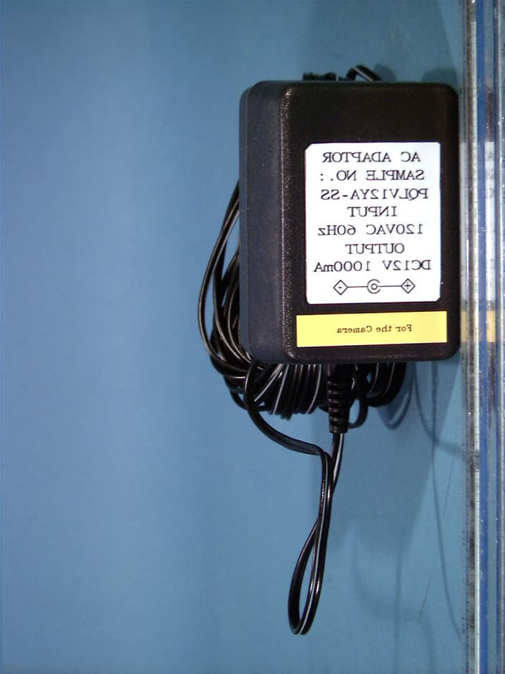
Click to zoom
Application Details
- Equipment Class
- DSS - Part 15 Spread Spectrum Transmitter
- Date of Grant
- Apr 02, 2002
- Application Purpose
- Original Equipment
- Date of Application
- Apr 02, 2002
- Equipment Note
- Wireless LAN Network Camera
- Frequency Range
- 2412.00000000 - 2462.00000000
- Country
- United States
Documents & Files
Document Text
Text extracted from the exhibit documents filed with the FCC. Open a document above to read the original.
Block Diagram
Test Block Diagram: LAPTOP PERSONAL COMPUTER KX-HCM270 RF BLOCK Σ S Hewlett Packard HPESG D4000A Signal Generator J Spectrum Analyzer Power Meter LAPTOP PERSONAL COMPUTER KX-HCM270 RF BLOCK Shield Room 6 dB Resistive Splitters Step Attenuators Variable Attenuator
External Photos
© 2002 PCTEST Lab Matsushita Electric Industrial Co. Ltd. NVLAP Lab Code: 100431-0 FCC ID: ACJ96NKX-HCM270 DSS Network Camera © 2002 PCTEST Lab Matsushita Electric Industrial Co. Ltd. NVLAP Lab Code: 100431-0 FCC ID: ACJ96NKX-HCM270 DSS Network Camera © 2002 PCTEST Lab Matsushita Electric Industrial Co. Ltd. NVLAP Lab Code: 100431-0 FCC ID: ACJ96NKX-HCM270 DSS Network Camera © 2002 PCTEST Lab Matsushita Electric Industrial Co. Ltd. NVLAP Lab Code: 100431-0 FCC ID: ACJ96NKX-HCM270 DSS Network Camera
ID Label/Location Info
© 2002 PCTEST Lab FCC ID SAMPLE LABEL & LOCATION LABELLING REQUIREMENTS PER §§ 2.925 The Label shown shall be permanently affixed at a conspicuous location on the device and be readily visible to the user at the time of purchase. (SEE NEXT PAGE) FCC ID: ACJ96NKX-HCM270
Internal Photos
© 2002 PCTEST Lab Matsushita Electric Industrial Co. Ltd. NVLAP Lab Code: 100431-0 FCC ID: ACJ96NKX-HCM270 DSS Network Camera © 2002 PCTEST Lab Matsushita Electric Industrial Co. Ltd. NVLAP Lab Code: 100431-0 FCC ID: ACJ96NKX-HCM270 DSS Network Camera © 2002 PCTEST Lab Matsushita Electric Industrial Co. Ltd. NVLAP Lab Code: 100431-0 FCC ID: ACJ96NKX-HCM270 DSS Network Camera © 2002 PCTEST Lab Matsushita Electric Industrial Co. Ltd. NVLAP Lab Code: 100431-0 FCC ID: ACJ96NKX-HCM270 DSS Network Camera © 2002 PCTEST Lab Matsushita Electric Industrial Co. Ltd. NVLAP Lab Code: 100431-0 FCC ID: ACJ96NKX-HCM270 DSS Network Camera © 2002 PCTEST Lab Matsushita Electric Industrial Co. Ltd. NVLAP Lab Code: 100431-0 FCC ID: ACJ96NKX-HCM270 DSS Network Camera © 2002 PCTEST Lab Matsushita Electric Industrial Co. Ltd. NVLAP Lab Code: 100431-0 FCC ID: ACJ96NKX-HCM270 DSS Network Camera © 2002 PCTEST Lab Matsushita Electric Industrial Co. Ltd. NVLAP Lab Code: 100431-0 FCC ID: ACJ96NKX-HCM270 DSS Network Camera © 2002 PCTEST Lab Matsushita Electric Industrial Co. Ltd. NVLAP Lab Code: 100431-0 FCC ID: ACJ96NKX-HCM270 DSS Network Camera © 2002 PCTEST Lab Matsushita Electric Industrial Co. Ltd. NVLAP Lab Code: 100431-0 FCC ID: ACJ96NKX-HCM270 DSS Network Camera © 2002 PCTEST Lab Matsushita Electric Industrial Co. Ltd. NVLAP Lab Code: 100431-0 FCC ID: ACJ96NKX-HCM270 DSS Network Camera
RF Exposure Info
RF Exposure Measurement 1. Introduction 2.4 GHz frequency band is regarded specially as a dangerous band for its heating harmfulness to the human body. That’s why microwave oven is operating in this frequency band. The manufacturer whose product is working in this frequency band is obligatory to prove the harmfulness of this product. In this document, we try to prove the safety of radiation harmfulness to the human body. The limit for the Maximum Permissible Exposure (MPE) specified in FCC 1.120 is followed. The Gain of the antenna, used in this product, is measured by a power meter. Through the Friis transmission formula and the maximum gain of the antenna, we can calculate the distance, away from the product, where the limit of MPE is reached. 2. RF Exposure Limit According to FCC 1.1310: The criteria listed in the following table shall be used to evaluate the environmental impact of human exposure to radio-frequency (RF) radiation as specified in 1.1307(b) LIMITS FOR MAXIMUM PERMISSIBLE EXPOSURE (MPE) Frequency Range (MHz) Electric Field Strength (V/m) Magnetic Field Strength (A/m) Power Density (mW/cm 2 ) Average Time (Minutes) (A) Limits for Occupational / Control Exposures 300-1500 ... ... F/300 6 1500-100,000 ... ... 5 6 (B) Limits for General Population / Uncontrolled Exposure 300-1500 ... ... F/1500 6 1500-100,000 ... ... 1.0 30 F = Frequency in MHz 3. Friis Formula Friis transmission formula : Pd = (Pout*G) / (4*pi*r 2 ) Where Pd = power density in mW/cm 2 Pout = output power to antenna in mW G = gain of antenna in linear scale Pi = 3.1416 R =distance between observation point and center of the radiator in cm Pd is the limit of MPE, 1mW/cm 2 . If we know the maximum Gain of the antenna and the total power input to the antenna, through the calculation, we will know the distance r where the MPE limit is reached. Ref.: David K. Cheng, Field and Wave Electromagnetics, Second Edition, Page 640, Eq. (11.133). 4. EUT Operating Condition Software provided by client enabled the EUT to transmit and receive data at lowest, middle and highest channel individually. 5. Climate Condition The temperature and the related humidity: 22°C and 78% RH 6. Test Results 6.1 Output Power into Antenna & RF Exposure Distance: Channel Channel Frequency (MHz) Output Power to Antenna (mW) Minimum Allowable Distance from skin (cm) 1 2412 85 6.76
RF Exposure Info
15.247(E) PROCESSING GAIN (FROM PANASONIC) Product Name: KX-HCM270 Limits: The processing gain of a direct sequence system shall be at least 10 dB. The processing gain shall be determined from the ratio in dB of the signal-to-noise ratio with the system spreading code turned off to the signal-to-noise ratio with the system spreading code turned on, as measured at the demodulated output of the receiver. Test Equipment: MS2602A Spectrum analyzer HP ESG D4000A signal generator HP437B Power meter HP8494A attenuator 1dB steps HP8495B attenuator 10dB steps PD28-0725-SMA power spiltter Laptop Computer Panasonic CF-M1V Theoretical calculation: 1. THEORETICAL PROCESS GAIN FOR DBPSK & DQPSK This value and the measured J/S ratio are used in the following equation to calculate the Process Gain (Gp) of the system. Gp = (S/N)o+Mj+Lsys Where: (S/N)o: Theoretical signal to noise ratio required to maintain the normal operation just before the BER appears. In real measurements the maximum error of 0.001 is allowed in an ideal system using their modulation scheme with all codes turned off (i.e. no spreading or processing gain). Mj: Maximum jammer to Signal Ratio that recorded at the detected BER. Lsys: System losses such as non-ideal synchronization, tracking circuitry, non-optimal baseband receiver filtering and etc... These losses can be in excess of 3 dB for each transmitter and receiver pair. For the purpose of this processing gain calculation we assume a Lsys at its minimum value of 2 dB. Ref.: Dixon, R, Spread Spectrum Systems . (New York: Wiley, 1984), Chapter 1. • (S/N)o: Refer to attached curves, BER versus (S/N)o for Differential Coherent Detection of Differentially EncodedBPSK • Processing gain Gp = (S/N)o + Lsys + Mj = (S/N)o + 2 + Mj 2. THEORETICAL PROCESS GAIN FOR CCK MODULATION The Processing gain is related to be jamming margin as follows: Gp=(S/N)output + (J/S) + Lsystem Where BER reference is the reference bit error ratio with its corresponding, theoretical output signal to noise ratio per symbol, (S/N)output, (J/S) is the jamming margin(jamming signal power relative to desired signal power), and Lsystem are the system implementation losses.. The maximum allowed total system implementation loss is 2 dB. The ISL3873 direct sequence spread spectrum baseband processor use CCK modulation which is a form of M-ary Orthogonal Keying. The Probability of error for generalized M-ary orthogonal signaling using coherent demodulation is given by: figure.1 1000 byte PER vs. Es/No PPQz Ez dz ec b M S N =−=−−+ − − − ∞ ∫ 11 1 2 212 2 1 2 1 2 01 0 π η ()exp Therefore For the case of the ISL3873, the bit rates are 1, 2, 5.5, and 11 Mbps. The corresponding symbol rates are 1, 1, 1.375,and 1.375 MSps. The chip rate is always 11 MCps, so the ratio of chip rate to symbol rate is 11:1 for the 1 and 2 Mbps rates and 8:1 for the 5.5 and 11 Mbps rates. Since the symbol rate to bit rate is less than 10 for the higher rates, we supply the theoretical processing gain calculation for these cases where spread spectrum processing gain with embedded coding gain is utilized. This is reasonable in that they cannot be separated in the demodulation process. If a separable FEC coding scheme were used, we would not be comfortable making this assertion. As can be seen from the curve of figure 1, the Es/N0 is 16.4 dB at the PER of 8%. This PER can be related to a BER of 1e-5 on 1000 byte packets. With 8 bits per symbol, the Eb/N0 is then 7.4 dB or 9 dB less than the Es/N0. It is well known that the Eb/N0 of BPSK is 9.6 dB for 1e-5 BER, so therefore the coding gain of CCK over BPSK is 2.2 dB. We add this to the processing gain of 9 dB to get 11.2 dB overall processing gain for the CW jammer test. Test Procedures: Obtain the simplex link shown. Perform all independent instrumentation calibrations prior to this procedure. Set operating power levels using fixed and variable attenuators in system to meet the following objectives: 1. Signal Power at receiver approximately -60 dBm (above thermal sensitivity such that thermal noise does not cause bit errors). 2. Signal Power at power meter between -20 and -30 dBm for optimal linearity. 3. Use spectrum analyzer to monitor test. 4. Ensure that CW Jammer generator RF output is disabled and measure the power at the power meter port using the power meter. This is the relative signal power, Sr . 5. Disable Transmitter, and set CW Jammer generator RF output frequency equal to the carrier frequency and enable generator output. Set reference CW Jammer power level at power meter port 8.4 dB below Sr (minimum J/S, or 10 dB processing gain reference level). Note the power level setting on the generator, this is the reference CW Jammer power setting, Jr. 6. Disable CW Jammer, re-establish link. PER test should be operating essentially error-free. 7. Enable CW Jammer at the reference power level and verify that the PER test indicates a PER of less than 8%. 8. Alternatively, adjust the CW Jammer level to that which causes 8% PER and verify that the S/J is less than 8.4 dB. 9. Repeat step 7 for uniform steps in frequency increments of 50 kHz across the receiver passband with the CW Jammer. In this case the receiver passband is +8.5 MHz. The number of points where the PER fails to achieve 8% (is higher than 8%) is determined and if this is above 20% of the total, the test is failed otherwise it is passed. The margin by which the radio passes the test (for informational purposes) can be determined from the average of the remaining points' PERs scaled on the PER curve above. The numerical data associated with the following radio channels is tabulated and presented for Channel 1: 2412 MHz (low channel of the band) Channel 6: 2437 MHz (middle channel of the band) Channel 11: 2462 MHz (high channel of the band) Test setup: as shown at next page Test Data: Processing gain test result summary Channel Frequency Data rate(Mbps) Worst point of the 8% FER (Limit is 20%) Resul…
Text truncated - open the document above for the full version.
Test Report
PCTEST PT. 15.247 REPORT EVALUATION REPORT Reviewed By: Quality Manager Test Report S/N: 15.220214068.ACJ Test Dates: FEB. 21-22, 2002 EUT Type: NETWORK CAMERA FCC ID: ACJ96NKX-HCM270 Page 1 of 19 PCTEST Engineering Laboratory, Inc. 66606660--B Dobbin Road B Dobbin Road •• Columbia, MD 21045 Columbia, MD 21045 •• U.S.A. U.S.A. TEL (410) 290TEL (410) 290--6652 6652 •• FAX (410) 290 FAX (410) 290--66546654 http://www.pctestlab.comhttp://www.pctestlab.com CERTIFICATE OF COMPLIANCE Matsushita Electric Industrial Co., Ltd. Dates of Tests: February 21-22, 2002 1006 Oaza Kadoma Test Report S/N: 15.220214068.ACJ Kadoma, Osaka 571 Japan Test Site: PCTEST Lab, Columbia MD Attention: Rich Mullen (PSCD) N. Yoshizumi-Kyushu MEICL FCC ID ACJ96NKX-HCM270 APPLICANT Matsushita Electric Industrial Co., Ltd. FCC Rule Part(s): § 15.247; ANSI C-63.4 (1992) Classification: Spread Spectrum Transceiver (DSS) Method/System: Direct Sequence System (DSS) Equipment Type: Network Camera Frequency Range: 2412.0 - 2462.0 MHz Model No(s).: KX-HCM270 Max. RF Power: 0.085W (EIRP) This equipment has been shown to be capable of compliance with the applicable technical standards as indicated in the measurement report and was tested in accordance with the measurement procedures specified in ANSI C-63-4. I attest to the accuracy of data. All measurements reported herein were performed by me or were made under my supervision and are correct to the best of my knowledge and belief. I assume full responsibility for the completeness of these measurements and vouch for the qualifications of all persons taking them. PCTEST certifies that no party to this application has been denied the FCC benefits pursuant to Section 5301 of the Anti-Drug Abuse Act of 1988, 21 U.S.C. 862. 220214068.ACJ PCTEST PT. 15.247 REPORT EVALUATION REPORT Reviewed By: Quality Manager Test Report S/N: 15.220214068.ACJ Test Dates: FEB. 21-22, 2002 EUT Type: NETWORK CAMERA FCC ID: ACJ96NKX-HCM270 Page 2 of 19 TABLE OF CONTENTS SCOPE 3 INTRODUCTION (SITE DESCRIPTION) 4 PRODUCT INFORMATION 5 DESCRIPTION OF TESTS A. CONDUCTED EMISSIONS 6 B. RADIATED EMISSIONS 7 C. RESTRICTED BANDS 8 D. ANTENNA REQUIREMENT 9 E. DIRECT SEQUENCE BANDWIDTH 10 F. MAXIMUM PEAK POWER OUTPUT 11 G. POWER DENSITY 12 RADIATED MEASUREMENTS (FUNDAMENTAL & HARMONICS) 13-15 RADIATED MEASUREMENTS (RESTRICTED BAND) 16 FREQUENCY MEASUREMENTS (SPURIOUS) 17 LIST OF TEST EQUIPMENT 18 CONCLUSION 19 APPENDIX A - LABELLING REQUIREMENTS APPENDIX B - PLOTS OF EMISSIONS APPENDIX C - PHOTOGRAPHS OF TEST SET-UP APPENDIX D - EUT PHOTOGRAPHS APPENDIX E - PROCESSING GAIN APPENDIX F - MPE DATA APPENDIX G - USERS MANUAL PCTEST PT. 15.247 REPORT EVALUATION REPORT Reviewed By: Quality Manager Test Report S/N: 15.220214068.ACJ Test Dates: FEB. 21-22, 2002 EUT Type: NETWORK CAMERA FCC ID: ACJ96NKX-HCM270 Page 3 of 19 MEASUREMENT REPORT Scope - Measurement and determination of electromagnetic emissions (EME) of radio frequency devices including intentional and/or unintentional radiators for compliance with the technical rules and regulations of the Federal Communications Commission. §2983(a) General Information Applicant Name: Matsushita Electric Industrial Co., Ltd. Address: 1006 Oaza Kadoma Kadoma, Osaka 571 JAPAN Attention: Rich Mullen (PSCD) • FCC ID: ACJ96NKX-HCM270 • Class: Spread Spectrum Transceiver (DSS) • Type: Network Camera • Freq. Range: 2412.0 - 2462.0 MHz • Method/System: Direct Sequence System (DSS) • Model No(s): KX-HCM270 • Max. RF Output Power: 0.085 W • Power Supply: AC Adapter Panasonic Model: PQLV12Y Input: 120V ~ 60Hz Output: 12V ~ 850mA • USOC Jack: RJ-45 • Rule Part(s): § 15.247 • Dates of Tests: February 21-22, 2002 • Place of Tests: PCTEST Lab, Columbia, MD U.S.A. • Test Report S/N: 15.220214068.ACJ NOTE: The receiver portion was tested and complies with Part 15B under the verification procedure. PCTEST PT. 15.247 REPORT EVALUATION REPORT Reviewed By: Quality Manager Test Report S/N: 15.220214068.ACJ Test Dates: FEB. 21-22, 2002 EUT Type: NETWORK CAMERA FCC ID: ACJ96NKX-HCM270 Page 4 of 19 INTRODUCTION The measurement procedure described in American National Standard for Methods of Measurement of Radio- Noise Emissions from Low-Voltage Electrical and Electronic Equipment in the Range of 9kHz to 40GHz (ANSI C63.4-1992) and FCC Public Notice dated July 12, 1995 entitled “Guidance on Measurement for Direct Sequence Spread Spectrum Systems” were used in the measurement of Panasonic Network Camera model: KX- HCM270. These measurement tests were conducted at PCTEST Engineering Laboratory, Inc. facility in New Concept Business Park, Guilford Industrial Park, Columbia, Maryland. The site address is 6660-B Dobbin Road, Columbia, MD 21045. The test site is one of the highest points in the Columbia area with an elevation of 390 feet above mean sea level. The site coordinates are 39° 11'15" N latitude and 76° 49'38" W longitude. The facility is 1.5 miles North of the FCC laboratory, and the ambient signal and ambient signal strength are approximately equal to those of the FCC laboratory. There are no FM or TV transmitters within 15 miles of the site. The detailed description of the measurement facility was found to be in compliance with the requirements of § 2.948 according to ANSI C63.4 on October 19, 1992. PCTEST Location The map at right shows the location of the PCTEST Lab, its proximity to the FCC Lab, the Columbia vicinity area, the Baltimore-Washington International (BWI) airport, and the city of Baltimore, and the Washington, D.C. area. (see Figure1). Figure 1. Map of the Greater Baltimore and Metropolitan Washington, D.C. area. PCTEST PT. 15.247 REPORT EVALUATION REPORT Reviewed By: Quality Manager Test Report S/N: 15.220214068.ACJ Test Dates: FEB. 21-22, 2002 EUT Type: NETWORK CAMERA FCC ID: ACJ96NKX-HCM270 Page 5 of 19 PRODUCT INFORMATION Equipment Description: The Equipment under test (EUT) is the Panasonic Network Camera system using spread spectrum direct sequence and time division…
Text truncated - open the document above for the full version.
Test Setup Photos
© 2002 PCTEST Lab Matsushita Electric Industrial Co. Ltd. NVLAP Lab Code: 100431-0 FCC ID: ACJ96NKX-HCM270 DSS Network Camera © 2002 PCTEST Lab Matsushita Electric Industrial Co. Ltd. NVLAP Lab Code: 100431-0 FCC ID: ACJ96NKX-HCM270 DSS Network Camera © 2002 PCTEST Lab Matsushita Electric Industrial Co. Ltd. NVLAP Lab Code: 100431-0 FCC ID: ACJ96NKX-HCM270 DSS Network Camera © 2002 PCTEST Lab Matsushita Electric Industrial Co. Ltd. NVLAP Lab Code: 100431-0 FCC ID: ACJ96NKX-HCM270 DSS Network Camera
Contact Information
Applicant
Ben Botros(Project Manager)
Technical Contact
PCTEST Engineering Lab., Inc.Randy Ortanez
[email protected]410-290-6652
6660-B Dobbin Road · Columbia, Maryland · United States
Test Firm
PCTEST Engineering Laboratory, Inc.Randy Ortanez
Technical Specifications
| # | Rule Parts | Frequency Range | Power Output |
|---|---|---|---|
| 1 | 15C | 2.41 GHz - 2.46 GHz | 85.00 mW |
Other Applications from Panasonic Corporation of North America
ACJ-EAH-A1000
Aug 19, 2026Digital Wireless Stereo Headphones
Equipment Class
DSS - Part 15 Spread Spectrum TransmitterACJ9TGFZVNF3G1
Jun 16, 2026Contactless Smart Card Reader
Equipment Class
DXX - Part 15 Low Power Communication Device Transmitter
ACJ932AM2301
Jan 29, 2025Car AV Control Unit for CDC
Equipment Class
DTS - Digital Transmission SystemACJ96NKX-TGEA60B
Aug 13, 2024DECT Handset
Equipment Class
PUE - Part 15 Unlicensed PCS portable Tx held to earACJ96NKX-TGE630B
Aug 12, 2024DECT Base Unit
Equipment Class
PUB - Part 15 Unlicensed PCS Base Station