ACJ96NKX-TDA0142Base unit for FHSS phone system
Panasonic Corporation of North America
Click to zoom
Application Details
- Equipment Class
- DSS - Part 15 Spread Spectrum Transmitter
- Date of Grant
- Feb 25, 2002
- Application Purpose
- Original Equipment
- Date of Application
- Oct 22, 2001
- Equipment Note
- Base unit for FHSS phone system
- Frequency Range
- 2401.05600000 - 2479.68000000
- Country
- United States
Documents & Files
Document Text
Text extracted from the exhibit documents filed with the FCC. Open a document above to read the original.
Users Manual
Installation Manual13 For Cell Station CAUTION Any changes or modifications not expressly approved by the party responsible for compliance could void user’s authority to operate this device. Note This equipment has been tested and found to comply with the limits for a Class B digital device, pursuant to Part 15 of the FCC Rules. These limits are designed to provide reasonable protection against harmful interference in a residential installation. This equipment generates, uses, and can radiate radio frequency energy and, if not installed and used accordance with the instructions, may cause harmful interference to radio communications. However, there is no guarantee that interference will not occur in a paticular installation. If this equipment does cause harmful interference to radio or television reception, which can be determined by turning the equipment off and on, the user is encouraged to try to correct the interference by one or more of the following measures: • Reorient or relocate the receiving antenna. • Increase the separation between the equipment and receiver. • Connect the equipment into an outlet on a circuit different from that to which the receiver is connected. • Consult the dealer or an experienced radio/TV technician for help. Some wireless telephones operate at frequencies that may cause interference to nearby TVs and VCRs. To minimize or prevent such interference, the base of the wireless telephone should not be placed near or on top of a TV or VCR. If interference is experienced, move the wireless telephone further away from the TV or VCR. This will often reduce, or eliminate, interference. Operating near 2.4 GHz electrical appliances may cause interference. Move away from the electrical appliances. CAUTION To comply with FCC RF exposure requirements in uncontrolled environment: • This equipment must be installed and operated in accordance with provided instructions and a minimum 20 cm spacing must be provided between antenna and all person’s body (excluding extremities of hands, wrist and feet) during wireless modes of operation. • This transmitter must not be co-located or operated in conjunction with any other antenna or transmitter. Medical – consult the manufacturer of any personal medical devices, such as pacemakers, to determine if they are adequately shielded from external RF(radio frequency) energy. (The unit operates in the frequency range of 2401 MHz to 2480 MHz, and the power output level can range from 0.004 watts to 0.4 watts.) Do not use the unit in health care facilities if any regulations posted in the area instruct you not to do so. Hospitals or health care facilities may be using equipment that could be sensitive to external RF(radio frequency) energy.
Attestation Statements
FCC ID : ACJ96NKX-TDA0142 FACTORY CONTROL NO. : KMSC-01-F103 1 of 1 EXHIBIT E DESCRIPTION OF ELECTRICAL CIRCUITRY A) When receiving a call to Portable Station (1) When there is an incoming call to Portable Station, PBX sends paging information to IC113 via cable. IC113 is responsible for wired data transmission between Cell Station and PBX. (2) Paging information is received at IC113 and sent to IC112. IC 112 is a HDLC protocol controller for high reliability data communication. Paging information is formatted at IC112. (3) IC102 (CPU) reads paging information in IC112 by bus access and writes paging information onto IC100 (Base Band IC). In IC100 paging information is combined with voice data, framed, and sent to RF circuit as TXDA signal. (4) Voice data (ADPCM) is also transferred to IC113 via cable. Voice data is fed to pin DSTI of IC101 and formatted to fit to IC100 data format. Then Voice data is fed to pin DDN of IC100. Voice data is combined with paging information in IC100 and fed to RF circuit as TXDA signal. TXDA signal is filtered at analog filter composed of FLT1, FLT2, R113, R114, R115, C120, C121 and C122 and fed to RF circuit. (5) The filtered TXDA signal is converted into 2.4GHz FSK (Frequency Sift Keying) modulation signal at the inside of RFIC (IC201). After amplified by RF Power Amp (IC101), FSK modulation signal goes through band pass filter (FIL101) and then outputs to the antenna. B) When making a call from Portable Station (1) Portable Station sends call information to Cell Station by radio. (2) RF signal from Portable Station (KX-TD7690) is received by an antenna, passes through the 2.4GHz band pass filter FIL101, and then the signal is fed to pin (RF and RFX) of RF-IC (IC201). (3) The RF signal fed to RF-IC passes through LNA (Low Noise Amplifier) Low IF band pass filter and is demodulated to digital signal by demodulator. Then the demodulated signal is fed to base band IC (IC100) from RXDA pin. (4) In IC100 call information and voice data (ADPCM) is extracted from demodulated signal. (5) IC102 (CPU) reads call information from IC100 and writes call information onto IC112. Then call information is formatted and transferred to IC113. And Call information is transmitted to PBX via cable. (6) On the other hand voice data (ADPCM) is extracted at IC100 and fed to IC101 through pin DUP. Voice data is formatted to fit to IC113 data format and fed to pin DSTI of IC113. Voice data is transmitted from IC113 to PBX via cable.
Attestation Statements
FCC ID : ACJ96NKX-TDA0142 FACTORY CONTROL NO. : KMSC-01-F103 1 of 1 EXHIBIT A STATEMENT OF SECURITY CODE This wireless system has 1000 billion digital security coding combinations that are provided by the following means: • Provided with 40 bits (1000 billion) for security codes.. • When shipped from the factory, the security code is decided by the manufacturer.
Attestation Statements
Matsushita Electric Corporation of America Product Safety & Compliance Division 1 Panasonic Way, 4B-8 Zameel Shahat Secaucus, NJ 07094 Project Engineer Panasonic Quasar Technics Fax: (201) 392-4564 Tel: (201) 392-4161 e-mail: [email protected] January 10, 2002 KMSC-01F103 731 Confirmation Number: EA559209 To: Joseph Dichoso / FCC Application Processing Branch From: Zameel Shahat / Matsushita Electric Corp. of America EA559209 Please note following answers to your above referenced correspondence inquiry: 1- Q) A) The measured conducted power in page 17 is 295mW. This is a typing error it should be 219mW same as measurement result at page 32 of the test report. We will submit the test report correction. Also we will change the Item 11 on page 4 as shown below (present) Typical TX power 125.9mW(21.0dBm) (after changed ) Measured TX power(conducted) 219mW(23.4dBm) 2- Q)What is the gain? Describe the antenna. How does it get 4.77 dBi gain? A) *Antenna gain (numeric) = EIRP /TP Antenna gain (dB) = 10log 10 (EIRP /TP) EIRP is the max radiated power and TP is the max transmitted power. * this antenna is half-wave length dipole. * The following is the calculated result CH Frequency EIRP TP Antenna gain(Geut) No. (MHz) (W) (W) (dBi) 00 2401.056 0.656 0.219 4 .7 7 ------------------------------------------------------------------------------------------------- 46 2440.800 0.585 0.204 4.57 91 2479.680 0.498 0.186 4.27 Sample of calculated result at 2401,056 MHz, as the Maximum point: EIRP = 28.17 dBm = l0log 10 (0.656) + 30 TP = 23.40 dBm = l0log 10 (0.219) + 30 Result = 4.77 dBi 3- Q) Provide AC power line tests. A) The power source of Cell station is supplied from PBX unit.(DC40V,80mA maximum) (Please refer to the attached file. "MKSC-01-F103(TDA0142).pdf") Therefore this product have no direct connection to the AC Line. 4- Q) Provide RF safety calculations with the correct output power and antenna gain. A) The Maximum Peak Power (EIRP) is measured as 656mW on page 30 on test eport. The EIRP have already included the antenna gain. Considering the power density, power should be averaged the EIRP in the total transmitting time of Whole TDMA frame. We calculated averaged radiated power using below steps. (Calculation step) ****************************************************************** The TDMA frame structure of this system is described in the attached file named "MKSC-01-F103(TDMA frame structure).pdf ". According to this description, maximum transmitting time of RF carrier is calculated from below Steps. a. Transmitting time(each slot) :Tst Tst = transmission slot time(ex. t0 ,t1,t2,t3,t4))-Guard Space time = 833 (micro seconds) - 96(micro seconds) =737 (micro seconds) Considering the rising or falling time of RF output at power amplifier, actual Tst is approximately 750 (micro seconds) . b. Maximum time of transmitting carrier :Tmax Tmax = Tst * 4 slots = 750 micro seconds * 4 = 3000 micro seconds= 3( msec ) c. Whole time of TDMA frame is 10msec. So The EIRP is averaged using the ratio means Tmax /10msec. Averaging Ratio = 3/10. d. As a result, Actual radiated Power is EIRP* 3/10 = 656 * 3/10 = 196.8 mW From the above the distance between observation point and center of radiator in cm (R) Can be calculated using the formula R 2 = EIRP/4ps S = Power density in mW/cm 2 R 2 = 196.8/4p*1 R= 3.96 cm << 20 cm Our operation instruction will have the following in page 14 "CAUTION: To comply with FCC RF exposure requirements, the base unit should be installed with its antenna located at 20 cm or more from persons.” This enable the subject device to classified as a mobile unit and exempt from SAR requirement. 5- Q) It appears that the device will not comply with the Restricted band requirements at 2483.5-2500 MHz. The emission is only 49 dB down from the peak of the fundamental emission. The fundamental emission was measured with a 100 kHz RBW. It must be measured with a 1 MHz RBW and VBW. Therefore, the level of the fundamental will be higher than 123.4 dBuV/m and the level at 2483.5 MHz will be greater than 74 dBuV/m. A)We think the measurement condition of Band-edge compliance test described on test report could be adapted for FCC 15.247(C). The reason is following subjects. According to PUBLIC NOTICE document issued by FCC named" Filing and Measurement Guidelines for Frequency Hopping Spread Spectrum Systems", (Released March 30, 2000) the measurement setting and method for "Band- edge compliance of RF Conducted Emissions" is described as follows, “ Use the following spectrum analyzer setting: Span= wide enough to capture the peak level of the emission operating on the channel closest to the band edge , as well as any modulation products which fall outside of the authorized band of operation. RBW >= 1percent of the span.( When span is 10MHz, RBW is more than 100KHz) VBW>= RBW( if RBW is 100KHz, VBW is available for 300KHz)” In addition, We confirmed that the level of the fundamental does not change when using the 100KHz RBW from when using the 1MHz RBW. Therefore the level of the fundamental must be 122.2 dBuV/m at 91ch(2479.680MHz)and the level at 2483.5 MHz must be less than 74 dBuV/m. You have pointed out the fundamental level is 123.4dBuVm. But when we confirm the compliance of Band edge emission, we think reference fundamental level should be used the level of nearest channel(91ch) from band edge. If above requirements could be available now, we think band- edge emission level is complied for the regulation. 6- Q) Provide a few examples of the pseudorandom hop sequence. A) The Pseudo random Hopping sequence 1- The system operates the pseudo randomly hopping sequence that is given by random hopping sequence table. A dummy bearer that has broad cast information uses a table generated hop sequence. The sequence are generated by the following formula. Fx( i )= (Fo(i) + x)mod 75 The sequence index "i" in the above formula is incremented (mod 75) each frame. The value "x" is used to select the re…
Text truncated - open the document above for the full version.
Attestation Statements
Hopping Pattern of Dummy Bearer (total 75Patterns) index(i)*Pattern 0Pattern 1Pattern 2Pattern 3----Patten74 0012374 12728293026 23839404137 31415161713 42627282925 54950515248 61314151612 73334353632 87374757672 95556575854 101617181915 1112340 121112131410 135455565753 148910117 156465666763 1623451 174849505147 182829303127 196162636460 2045673 214041424339 226566676864 2367895 242324252622 256768697066 265758596056 274243444541 281213141511 292930313228 306263646561 313637383935 324748495046 3356784 347172737470 354344454642 363233343531 375657585955 382122232420 395960616258 403940414238 411516171814 425354555652 431819202117 444546474844 453738394036 467401273 476364656662 484647484945 4934562 505152535450 513132333430 527273747571 535859606157 5491011128 557071727369 563536373834 576970717268 582526272824 593435363733 605051525349 616061626359 626869707167 632223242521 645253545551 652425262723 664142434440 67789106 681718192016 693031323329 701920212218 71101112139 722021222319 736667686965 744445464743 *A index No. means sequential number of hop sequence. Each number described beside the index No. means Logical Channel Number. Each number of Logical Channel No table to be converted from physical channel No.from 00 to 91. The system selects the physical channels which have good communication quality to make up the Logical Channel No table. The physical channels is ranging from 00 to 91,on the other hand Logical Channel No. has a range from 00 to 74. This results in 16 physical channels that are not part of the normal sequence ,and these are reserved as 'spares'.
Attestation Statements
COMMERCIAL IN CONFIDENCE P/GLENEAGLES/DOC/SPEC/S10462/4.0 Page 21 APPENDIX D – LCG RANDOM HOPPING SEQUENCE The following table is the random channel sequence produced by the LCG random number generator. The sequence is 3000-long (arranged in a 300 × 10 table): 0 1 2 3 4 5 6 7 8 9 0 0 19 66 20 60 68 73 29 43 69 10 61 51 68 66 2 55 29 31 15 10 20 48 8 69 38 19 41 61 33 61 27 30 35 39 71 10 35 28 18 34 33 44 40 22 71 73 57 52 15 50 36 5 61 50 8 28 0 28 69 2 6 38 52 2 60 70 60 1 0 11 63 38 40 23 19 70 57 16 3 47 27 50 70 41 70 36 80 44 48 5 19 44 37 27 43 42 53 90 30 5 7 65 61 24 58 45 14 69 100 17 37 8 37 3 10 15 47 60 11 110 4 68 10 9 19 72 47 48 32 28 120 66 25 12 56 36 59 4 50 4 45 130 52 57 14 27 53 46 35 52 51 61 140 39 14 15 74 70 32 67 54 22 3 150 26 45 17 46 11 19 24 55 69 20 160 13 2 19 18 28 6 56 57 41 37 170 74 34 21 64 45 68 12 59 13 53 180 61 66 22 36 62 54 44 61 59 70 190 48 22 24 8 3 41 1 62 31 12 200 35 54 26 55 20 28 33 64 3 29 210 21 11 28 26 37 15 64 66 50 45 220 8 43 29 73 54 1 21 68 21 62 230 70 74 31 45 70 63 53 69 68 4 240 57 31 33 17 12 50 10 71 40 21 250 43 63 35 63 29 37 41 73 12 37 260 30 20 36 35 46 23 73 0 58 54 270 17 51 38 7 62 10 30 1 30 71 280 4 8 40 54 4 72 62 3 2 13 COMMERCIAL IN CONFIDENCE P/GLENEAGLES/DOC/SPEC/S10462/4.0 Page 22 290 65 40 42 25 21 59 18 5 49 29 300 52 72 43 72 38 45 50 7 20 46 310 39 28 45 44 54 32 7 8 67 63 320 26 60 47 16 71 19 39 10 39 5 330 12 17 49 62 13 6 70 12 11 21 340 74 49 50 34 30 67 27 14 57 38 350 61 5 52 6 46 54 59 15 29 55 360 48 37 54 53 63 41 16 17 1 72 370 34 69 56 24 5 28 47 19 48 13 380 21 26 57 71 22 14 4 21 19 30 390 8 57 59 43 38 1 36 22 66 47 400 70 14 61 15 55 63 68 24 38 64 410 56 46 63 61 72 50 24 26 10 5 420 43 3 64 33 14 36 56 28 56 22 430 30 34 66 5 30 23 13 29 28 39 440 17 66 68 52 47 10 45 31 0 56 450 3 23 70 23 64 72 1 33 47 72 460 65 55 71 70 6 58 33 35 18 14 470 52 11 73 42 22 45 65 36 65 31 480 39 43 0 14 39 32 22 38 37 48 490 25 0 2 60 56 19 53 40 9 64 500 12 32 3 32 73 5 10 42 55 6 510 74 63 5 4 14 67 42 43 27 23 520 61 20 7 51 31 54 74 45 74 40 530 47 52 9 22 48 41 30 47 46 56 540 34 9 10 69 65 27 62 49 17 73 550 21 40 12 41 6 14 19 50 64 15 560 8 72 14 13 23 1 51 52 36 32 570 69 29 16 59 40 63 7 54 8 48 580 56 61 17 31 57 49 39 56 54 65 590 43 17 19 3 73 36 71 57 26 7 600 30 49 21 50 15 23 28 59 73 24 610 16 6 23 21 32 10 59 61 45 40 620 3 38 24 68 49 71 16 63 16 57 COMMERCIAL IN CONFIDENCE P/GLENEAGLES/DOC/SPEC/S10462/4.0 Page 23 630 65 69 26 40 65 58 48 64 63 74 640 52 26 28 12 7 45 5 66 35 16 650 38 58 30 58 24 32 36 68 7 32 660 25 15 31 30 41 18 68 70 53 49 670 12 46 33 2 57 5 25 71 25 66 680 74 3 35 49 74 67 57 73 72 8 690 60 35 37 20 16 54 13 0 44 24 700 47 67 38 67 33 40 45 2 15 41 710 34 23 40 39 49 27 2 3 62 58 720 21 55 42 11 66 14 34 5 34 0 730 7 12 44 57 8 1 65 7 6 16 740 69 44 45 29 25 62 22 9 52 33 750 56 0 47 1 41 49 54 10 24 50 760 43 32 49 48 58 36 11 12 71 67 770 29 64 51 19 0 23 42 14 43 8 780 16 21 52 66 17 9 74 16 14 25 790 3 52 54 38 33 71 31 17 61 42 800 65 9 56 10 50 58 63 19 33 59 810 51 41 58 56 67 45 19 21 5 0 820 38 73 59 28 9 31 51 23 51 17 830 25 29 61 0 25 18 8 24 23 34 840 12 61 63 47 42 5 40 26 70 51 850 73 18 65 18 59 67 71 28 42 67 860 60 50 66 65 1 53 28 30 13 9 870 47 6 68 37 17 40 60 31 60 26 880 34 38 70 9 34 27 17 33 32 43 890 20 70 72 55 51 14 48 35 4 59 900 7 27 73 27 68 0 5 37 50 1 910 69 58 0 74 9 62 37 38 22 18 920 56 15 2 46 26 49 69 40 69 35 930 42 47 4 17 43 36 25 42 41 51 940 29 4 5 64 60 22 57 44 12 68 950 16 35 7 36 1 9 14 45 59 10 960 3 67 9 8 18 71 46 47 31 27 COMMERCIAL IN CONFIDENCE P/GLENEAGLES/DOC/SPEC/S10462/4.0 Page 24 970 64 24 11 54 35 58 2 49 3 43 980 51 56 12 26 52 44 34 51 49 60 990 38 12 14 73 68 31 66 52 21 2 1000 25 44 16 45 10 18 23 54 68 19 1010 11 1 18 16 27 5 54 56 40 35 1020 73 33 19 63 44 66 11 58 11 52 1030 60 64 21 35 60 53 43 59 58 69 1040 47 21 23 7 2 40 0 61 30 11 1050 33 53 25 53 19 27 31 63 2 27 1060 20 10 26 25 36 13 63 65 48 44 1070 7 41 28 72 52 0 20 66 20 61 1080 69 73 30 44 69 62 52 68 67 3 1090 55 30 32 15 11 49 8 70 39 19 1100 42 62 33 62 28 35 40 72 10 36 1110 29 18 35 34 44 22 72 73 57 53 1120 16 50 37 6 61 9 29 0 29 70 1130 2 7 39 52 3 71 60 2 1 11 1140 64 39 40 24 20 57 17 4 47 28 1150 51 70 42 71 36 44 49 5 19 45 1160 38 27 44 43 53 31 6 7 66 62 1170 24 59 46 14 70 18 37 9 38 3 1180 11 16 47 61 12 4 69 11 9 20 1190 73 47 49 33 28 66 26 12 56 37 1200 60 4 51 5 45 53 58 14 28 54 1210 46 36 53 51 62 40 14 16 0 70 1220 33 68 54 23 4 26 46 18 46 12 1230 20 24 56 70 20 13 3 19 18 29 1240 7 56 58 42 37 0 35 21 65 46 1250 68 13 60 13 54 62 66 23 37 62 1260 55 45 61 60 71 48 23 25 8 4 1270 42 1 63 32 12 35 55 26 55 21 1280 29 33 65 4 29 22 12 28 27 38 1290 15 65 67 50 46 9 43 30 74 54 1300 2 22 68 22 63 70 0 32 45 71 COMMERCIAL IN CONFIDENCE P/GLENEAGLES/DOC/SPEC/S10462/4.0 Page 25 1310 64 53 70 69 4 57 32 33 17 13 1320 51 10 72 41 21 44 64 35 64 30 1330 37 42 74 12 38 31 20 37 36 46 1340 24 74 0 59 55 17 52 39 7 63 1350 11 30 2 31 71 4 9 40 54 5 1360 73 62 4 3 13 66 41 42 26 22 1370 59 19 6 49 30 53 72 44 73 38 1380 46 51 7 21 47 39 29 46 44 55 1390 33 7 9 68 63 26 61 47 16 72 1400 20 39 11 40 5 13 18 49 63 14 1410 6 71 13 11 22 0 49 51 35 30 1420 68 28 14 58 39 61 6 53 6 47 1430 55 59 16 30 55 48 38 54 53 64 1440 42 16 18 2 72 35 70 56 25 6 1450 28 48 20 48 14 22 26 58 72 22 1460 15 5 21 20 31 8 58 60 43 39 1470 2 36 23 67 47 70 15 61 15 56 1480 64 68 25 39 64 57 47 63 62 73 1490 50 25 27 10 6 44 3 65 34 14 1500 37 57 28 57 23 30 35 67 5 31 1510 24 13 30 29 39 17 67 68 52 48 1520 11 45 32 1 56 4 24 70 24 65 1530 72 2 34 47 73 66 55 72 71 6 1540 59 34 35 19 15 52 12 74 42 23 1550 46 65 37 66 31 39 44 0 14 40 1560 33 22 39 38 48 26 1 2 61 57 1570 19 54 41 9 65 13 32 4 33 73 1580 6 11 42 56 7 74 64 6 4 15 1590 68 42 44 28 23 61 21 7 51 32 1600 55 74 46 0 40 48 53 9 23 49 1610 41 31 48 46 57 35 9 11 70 65 1620 28 63 49 18 74 21 41 13 41 7 1630 15 19 51 65 15 8 73 14 13 24 1640 2 51 53 37 32 70 30 16 60 41 COMMERCIAL IN…
Text truncated - open the document above for the full version.
Block Diagram
Cell Station(KX-TDA0142) BLOCK DIAGRAM2001/9/6 PMB4729ADPCM BYPASS 3.7V PSYNC D8-D15 SERIAL RF Burst Mode Controller RF Interface 4x ADPCM 2x Echo Cancel. 2x C-ID 4x Echo Suppre TX/RX DTMF Generator & Receiver 2x PMB2920 I/F IOM-2 IOM-2 I/F 4x PCM I/F uC I/F FLASH 4Mbit 16bit CPU(16Bit) (H8S/2340) MT8952 HDLC controller MT9171 DNIC Line I/F FPGA SYNC GEN FRAMER/DEFRAMER DECODER RAM 1Mit D0-D15 D8-D15 PF MONITOR DC/DC 40V 3.7V 3.3V SuperC 5V D8-D15 3.3V 5V 3.7V TCXO 19.2M A/DRSSI VCXO 10.368M TRIM D/A DIP SW Multi Frame 9.6M RESET IC DC/DC F/F Dual operation 10.24M 2.5V 2.5V IC100 IC113 IC112 IC101 IC102
Block Diagram
RF Block Diagram 5 Unit Ver.11 7 1234 Model Title Page KX-TDA0142 6 512346 2 : R CHP :32/33:N/A PLL & Control logic Demodulator VCO PD Stand by & Control logic S&H Low IF bandpass filter LNA IC201 PMB6618 ADRSSI RXDA SYCL SYDA SYEN FIL101 PQVFLFS2450B D101 BAR64- 05WRXDSG Loop filter Gausian filter TXDA SYRI PAON RXON IC102 Regu lator DRON 3.7V Q201 Voltage regulator Voltage regulator To CPU Block To CPU Block IC101 ITT2303GJ ANT1 ANT2 To CPU Block D124 Main Antenna Sub Antenna
Block Diagram
PBX Unit KX-TDA0142 (RF base) Power source DC40V,80mA (Supply from PBX) AC120V 60Hz Wireless Handset KX-TDA0142 Connection Diagram Cell Station Not required for AC power source.
Cover Letter(s)
Matsushita Electric Corporation of America Product Safety & Compliance Division 1 Panasonic Way, 4B-8 Zameel Shahat Secaucus, NJ 07094 Project Engineer Panasonic Quasar Technics Fax: (201) 392-4564 Tel: (201) 392-4161 e-mail: [email protected] February 8, 2002 KMSC-01F103 731 Confirmation Number: EA559209 To: Joseph Dichoso / FCC Application Processing Branch From: Zameel Shahat / Matsushita Electric Corp. of America Re: FCC ID ACJ96NKX-TDA0142 Applicant: Matsushita Electric Industrial Co Ltd Correspondence Reference Number: 21824 731 Confirmation Number: EA559209 Please note we submit the following files to the FCC 1- new test report corrections.pdf 2- AC test report 3- Dummy bearer hop table.pdf 4- Traffic bearer hop table.pdf 5- Installation manual corrections.pdf The following are the answers to your above referenced correspondence inquiry: 1- Q) The EIRP on page 16 does not agree with the EIRP of 656 mW. Also, A half wave dipole cannot have a gain of 4.77 dBi. Please correct these discrepancies. The EIRP must agree with the conducted output power + antenna gain. A) first, please see the corrected test report (new test report.pdf). We think it is very difficult avoiding difference from theoretical value and actual measured value. But our data in the test report is truly measured value. Below are our comments about this subject as a general knowledge of radiated power measurement. The measured field strength to calculate the EIRP does not agree with the EIRP calculated adding the transmitter power + antenna gain in the test report. For your question, it is understood that in the definition the EIRP measured in the substitution method is equal to the EIRP (adding the transmitter power + the antenna gain). In the test report, the both values are not equal by using the antenna gain indicated in page 4(less than 2.14dBi). Actually, they are not equal because of the chassis radiation and the secondary radiation. The completed condition of the equation is the ideal condition that the full transmitting power is cost in the transmitting antenna without reflection. The antenna gain indicated in page 4(less than 2.14dBi). is the specification in the antenna manufacturer. Less than 2.14dBi is not the value that is calculated from the EIRP and the transmitter power. Actually the chassis radiation and the secondary radiation add to the antenna radiation. In the radiation measurement, the multiplex radiation are included in the EIRP. This condition is not satisfied with the completed condition of the equation. 2- Q) Unless the device is battery operated, AC power line tests are required. Provide tests with a typical AC to DC adapter. A) I submit the AC test report to FCC today. 3- Q) You verified how the pseudorandom sequence is derived but you did not submit a few examples of the hop sequence as requeted. Please submit them. A)To establish the RF link, the system will broadcast a dummy bearer all the time it is powered up and operating. To avoid a sequence collision , the system select the one of proper Hopping pattern from Pattern 00 to pattern 74. (Please refer to 'Dummy bearer hop table.pdf'.) Once system have established the RF link to portable station, the Hopping sequence to be changed from dummy barer to traffic bearer. (Please refer to the 'Traffic bearer hop table.pdf'.) The table indicates the sequence of logical channel numbers. 4- Q) Provide conducted output power for the port not tested for verification purposes. If the data is higher, submit radiated tests. A) We have measured conducted power of two antenna ports. The port of 'ANT 1' is used for the submitted radiated data . Measuring condition(spectrum analyzer) RBW=1MHz, VBW=3MHz, SWP=20ms, MAX HOLD Result CH0 CH46 CH91 ANT1 23.06 22.66 22.35 ANT2 22.71 22.16 21.65 UnitdBm As you see the data above, the Power of ANT1 is higher than Power of ANT2. 5- Q) Mobile, 20 cm, non-colocated. A)we will have the following in our installation manual. “ CAUTION To comply with FCC RF exposure requirements in uncontrolled environment: • This equipment must be installed and operated in accordance with provided instructions and a minimum 20 cm spacing must be provided between antenna and all person’s body (excluding extremities of hands, wrist and feet) during wireless modes of operation. • This transmitter must not be co-located or operated in conjunction with any other antenna or transmitter.” Should you have any questions, please contact the undersigned. Thank you for your attention in this matter. Sincerely yours, Zameel Shahat Zameel Shahat Project Engineer
External Photos
FCC ID : ACJ96NKX-TDA0142 FACTORY CONTROL NO. : KMSC-01-F103 1 of 3 EXHIBIT D Photographs Figure 1 Front View Figure 2 Rear View FCC ID : ACJ96NKX-TDA0142 FACTORY CONTROL NO. : KMSC-01-F103 2 of 3 Figure 1 FCC ID : ACJ96NKX-TDA0142 FACTORY CONTROL NO. : KMSC-01-F103 3 of 3 Figure 2
ID Label/Location Info
FCC ID : ACJ96NKX-TDA0142 FACTORY CONTROL NO. : KMSC-01-F103 1 of 1 EXHIBIT B MARKINGS The unit provides with the following marking, or equivalent. This device complies with Part 15 of the FCC rules. Operation is subject to the following two conditions: (1) This device may not cause harmful interference, and (2) this device must accept any interference received, including interference that may cause undesired operation. NOTE: Above markings are shown on rear side of the unit.
Internal Photos
FCC ID : ACJ96NKX-TDA0142 FACTORY CONTROL NO. : KMSC-01-F103 1 of 3 EXHIBIT D-2 Photographs Figure 3 Internal view (Printed Wiring Board, Component side) Figure 4 Printed Wiring Board, Rear side FCC ID : ACJ96NKX-TDA0142 FACTORY CONTROL NO. : KMSC-01-F103 2 of 3 Figure 3 FCC ID : ACJ96NKX-TDA0142 FACTORY CONTROL NO. : KMSC-01-F103 3 of 3 Figure 4
Operational Description
Please read this manual before connecting the Hybrid IP PBX. Thank you for purchasing the Panasonic Model KX-TDA100/KX-TDA200, Hybrid IP PBX. KX-TDA100 Model No. KX-TDA200 Hybrid IP PBX Installation Manual System Components 2Installation Manual System Components System Components Table Model Description ShelvesKX-TDA100 KX-TDA200 Basic Shelf Basic Shelf Main Processor Card MPR (Main Central Processing Unit Circuit) Card MPR Option Cards KX-TDA0196 RMT (Remote Maintenance Trunk) Card Trunk CardsKX-TDA0180 KX-TDA0189 KX-TDA0193 KX-TDA0181 KX-TDA0187 KX-TDA0188 KX-TDA0184 KX-TDA0284 KX-TDA0288 KX-TDA0290 KX-TDA0290 KX-TDA0480 LCOT8 (8-port Loop Start Central Office Trunk) Card CID/PAY8 (8-port Caller ID / Pay Tone) Card CID8 (8-port Caller ID) Card LCOT16 (16-port Loop Start Central Office Trunk) Card T1 (T-1 Line Trunk) Card E1 (E-1 Line Trunk) Card E&M8 (8-port E&M) Card BRI4 (4-port ISDN Basic Rate Access Interface) Card BRI8 (8-port ISDN Basic Rate Access Interface) Card PRI30 (ISDN Primary Rate Access Interface) Card PRI23 (ISDN Primary Rate Access Interface) Card IP-GW4 (IP-Gateway Circuit) Card Extension Cards KX-TDA0170 KX-TDA0172 KX-TDA0171 KX-TDA0175 KX-TDA0174 KX-TDA0173 KX-TDA0143 KX-TDA0144 DHLC8 (8-port Digital Hybrid Line Circuit) Card DLC16 (16-port Digital Proprietary Line Circuit) Card DLC8 (8-port Digital Proprietary Line Circuit) Card MSLC16 (16-port SLT with Message Waiting Lamp Circuit) Card SLC16 (16-port SLT Circuit) Card SLC8 (8-port SLT Circuit) Card CSIF4 (4-port Cell Station Interface Circuit) Card CSIF8 (8-port Cell Station Interface Circuit) Card System Components Installation Manual3 Notice • There are some optional service cards and features which are not available for certain countries. Consult your authorised Panasonic dealer for detailed instructions. • The power supply capacity of the main unit may differ from the values described in this manual depending on the suffix of the model number, please consult your dealer for detailed information. Option CardsKX-TDA0190 KX-TDA0191 KX-TDA0161 KX-TDA0162 KX-TDA0164 KX-TDA0166 KX-TDA0410 OPB3 (Option Base 3 Circuit) Card MSG4 (Message Circuit) Card DPH4 (Doorphone Circuit) Card DPH2 (Doorphone Circuit) Card EIO4 (External I/O Circuit) Card ECHO16 (16-port Echo Cancelling Circuit) Card CTI-LINK (CTI-Link) Card Power Supply Unit KX-TDA0103 KX-TDA0104 L-Type Power Supply Unit M-Type Power Supply Unit System Components Table Model Description System Components 4Installation Manual System Components Table Model Description Digital Proprietary Telephones (DPTs) KX-T7625 KX-T7630 KX-T7633 KX-T7636 DPT with SP-PHONE (24-CO) DPT with SP-PHONE, 3-Line Display (24-CO) DPT with SP-PHONE, 3-Line Display (24-CO) DPT with SP-PHONE, 6-Line Display (24-CO) KX-T7520 KX-T7531 KX-T7533 KX-T7536 KX-T7550 KX-T7560 KX-T7565 DPT with SP-PHONE (12-CO) DPT with SP-PHONE, 1-Line Display (12-CO) DPT with SP-PHONE, 3-Line Display (12-CO) DPT with SP-PHONE, 6-Line Display (12-CO) DPT with MONITOR (12-CO) DPT with MONITOR (8-CO) DPT with SP-PHONE, 1-Line Display (8-CO) KX-T7420 KX-T7425 KX-T7431 KX-T7433 KX-T7436 KX-T7450 KX-T7451 DPT with SP-PHONE (12-CO) DPT with SP-PHONE (24-CO) DPT with SP-PHONE, 1-Line Display (12-CO) DPT with SP-PHONE, 3-Line Display (24-CO) DPT with SP-PHONE, 6-Line Display (24-CO) DPT with MONITOR (12-CO) DPT with MONITOR (4-CO) KX-T7220 KX-T7230 KX-T7235 KX-T7250 DPT with SP-PHONE (24-CO) DPT with SP-PHONE, 2-Line Display (24-CO) DPT with SP-PHONE, 6-Line Display (12-CO) DPT with MONITOR (6-CO) Analogue Proprietary Telephones (APTs) KX-T7320 KX-T7330 KX-T7350 APT with SP-PHONE (12-CO) APT with SP-PHONE, 1-Line Display (12-CO) APT with MONITOR (12-CO) KX-T7130APT with SP-PHONE, 1-Line Display (12-CO) KX-T7020 KX-T7030 KX-T7033 KX-T7050 KX-T7055 APT with SP-PHONE (12-CO) APT with SP-PHONE, 1-Line Display (12-CO)…
Text truncated - open the document above for the full version.
Contact Information
Applicant
Ben Botros(Project Manager)
Test Firm
Japan Quality Assurance Org.Katsumi Nishii
Technical Specifications
| # | Rule Parts | Frequency Range | Power Output | Tolerance |
|---|---|---|---|---|
| 1 | 15C | 2.40 GHz - 2.48 GHz | 219.00 mW | ppm |
Other Applications from Panasonic Corporation of North America
ACJ-EAH-A1000
Aug 19, 2026Digital Wireless Stereo Headphones
Equipment Class
DSS - Part 15 Spread Spectrum TransmitterACJ9TGFZVNF3G1
Jun 16, 2026Contactless Smart Card Reader
Equipment Class
DXX - Part 15 Low Power Communication Device Transmitter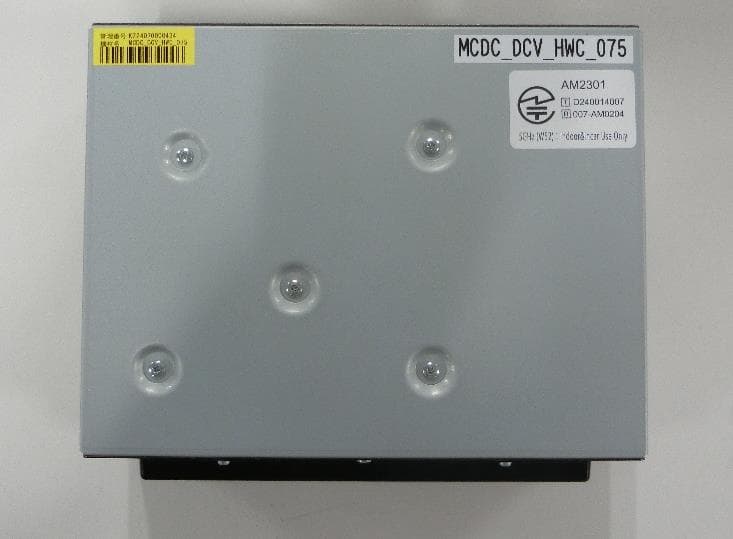
ACJ932AM2301
Jan 29, 2025Car AV Control Unit for CDC
Equipment Class
DTS - Digital Transmission SystemACJ96NKX-TGEA60B
Aug 13, 2024DECT Handset
Equipment Class
PUE - Part 15 Unlicensed PCS portable Tx held to earACJ96NKX-TGE630B
Aug 12, 2024DECT Base Unit
Equipment Class
PUB - Part 15 Unlicensed PCS Base Station