ACJ96NKX-UDT111DECT 6.0 Cordless Telephone Handset for SIP server or PBX
Panasonic Corporation of North America
Click to zoom
Application Details
- Equipment Class
- PUE - Part 15 Unlicensed PCS portable Tx held to ear
- Date of Grant
- May 23, 2012
- Application Purpose
- Original Equipment
- Date of Application
- May 23, 2012
- Equipment Note
- DECT 6.0 Cordless Telephone Handset for SIP server or PBX
- Frequency Range
- 1921.53600000 - 1928.44800000
- Country
- United States
Documents & Files
Document Text
Text extracted from the exhibit documents filed with the FCC. Open a document above to read the original.
Cover Letter(s)
EXHIBIT A STATEMENT OF SECURITY CODE This cordless telephone system has more than 1,000 billion combinations that are provided by the following means: ∑ Provided with 128 bits for security codes. ∑ When shipped from the factory, the security code is decided by the manufacture. It is memorized in a memory IC. ∑ Base and Handset knows each other’s security code information.
Cover Letter(s)
Panasonic Corporation of North America One Panasonic Way 4B-8 Secaucus, NJ 07094 Tel: 201-348-7758 / Fax: 201-392-4564 [email protected] Richard Mullen Group Manager Product Safety and Compliance Division Power of Attorney May 23, 2012 PCNF-12-F023 Federal Communication Commission Equipment Authorization Division / Application Processing Branch 7435 Oakland Mills Road Columbia, Maryland 21046 To whom it may concern; Panasonic Corporation of North America hereby authorizes Nemko AS to act on our behalf in all matters relating to the preparation of TCB Certification application for the below described product, which are in compliance with FCC Part 15D. Any and all acts carried out by Nemko AS on our behalf shall have the same effects as acts of our own for a period of one year from the date of this letter. Type Filing: Original Application for DECT 6.0 Cordless Telephone Handset for SIP Server or PBX Model KX-UDT111 Product Classification: Part 15 Unlicensed PCS Portable Tx Held to Ear (PUE) FCC ID Handset Unit ACJ96NKX-UDT111 FCC Rule Part: FCC Part 15, Subpart D 1 Frequency Range: 1921.536 ~ 1928.448 MHz RF Output Power: 0.065 Watts Power Supply: Battery Charger Cradle, Model PNLV226 and AC Adaptor, Model PNLV226 with switching power supply at 36 kHz Responsible Panasonic Corporation of North America Applicant & Grantee: One Panasonic Way, Secaucus, NJ 07094 FRN Number: 0003762242 Responsible Manufacturer: Panasonic System Networks Co., Ltd. Sincerely yours, Richard Mullen Richard Mullen Group Manager Panasonic Corporation of North America Product Safety and Compliance Division 1 The subject DECT 6.0 Cordless Telephone Handset was FCC Part 68 certified under US: ACJIPNANKX-UDT11. Also, it may be used with DECT Base Model KX-UDS124, which will be FCC Part 15D certified under FCC ID: ACJ96NKX-UDS124. Panasonic Corporation of North America One Panasonic Way 4B-8 Secaucus, NJ 07094 Tel: 201-348-7758 / Fax: 201-392-4564 [email protected] Richard Mullen Group Manager Product Safety and Compliance Division Request for Confidentiality May 23, 2012 PCNF-12-F023 Federal Communication Commission Equipment Authorization Division Application Processing Branch 7435 Oakland Mills Road Columbia, Maryland 21046 To whom it may concern; Type Filing: Original Application for DECT 6.0 Cordless Telephone Handset for SIP Server or PBX Model KX-UDT111 Product Classification: Part 15 Unlicensed PCS Portable Tx Held to Ear (PUE) FCC ID Handset Unit ACJ96NKX-UDT111 In accordance with provisions of Sections 0.457 and 0.459 of the Commission’s Rules and Section 552(b)(4) of the Freedom of Information Act, we request permanent confidentiality for exhibits, which contain: (1) Antennas Construction; (2) Description of Electrical Circuitry; (3) Schematic Diagrams of Handset Unit and RF Unit; and (4) Block Diagram. The transmitter is not user adjustable and does not have a Tune-Up Procedure. These exhibits contain proprietary, confidential and trade secrets material, which would not be routinely made available for public inspection. In accordance with FCC Public DA 04-1705, we request forty-five day short-term confidentiality, starting from the from the issuance of equipment authorization date, for exhibits, which contain: (1) External Photographs of Handset Unit and RF Unit; (2) Internal Photographs of Handset Unit and RF Unit; (3) Test Setup Photographs; and (4) User Manual. These exhibits contain pre-market information, which could give our competitors unfair advantage should this information be released before this product is actually introduced into the common marketplace. Sincerely yours, Richard Mullen Richard Mullen Group Manager Panasonic Corporation of North America Product Safety and Compliance Division
External Photos
EXHIBIT D-1 EXTERNAL PHOTOGRAPHS EXHIBIT D-1 EXTERNAL PHOTOGRAPHS
Internal Photos
EXHIBIT D-2 INTERNAL PHOTOGRAPHS PCB front PCB rear EXHIBIT D-2 INTERNAL PHOTOGRAPHS PCB rear, removed shield case of RF block RF block under the shield case
Parts List/Tune Up Info
20111222-307 M O D E L P A R T S L I S T (Ref.No.PNLPUDT111R1ZA-S2-REV004) MODEL: PNLPUDT111R1ZA-S2 STEP:D APPROVED DATE:2011/12/26 Panasonic System Networks Co., Ltd. APPLY: E_CLERK: M_CLERK: S_CLERK: O/P DATE:2012/01/10 LEVEL SORT ASSY CODE OR SUPLY PARTS RISK NOT USE PARTS NUMBER MAKER NUMBER REMARKS QT. UNIT PL S_RMKS S_SUM S_ID NOTE 1 PNLPUDT111R1ZA-S2 #1AJ1LPUDT111RZA 1 PC Inspection and Adjustment Standard 2 #1AJ1LPUDT111RZA #1AP1LPUDT111RZA 1 PC Manual & Auto Insert Part3 #1AP1LPUDT111RZA #1RE2LPUDT111RZA #1RE2 1 PC Reflow Process4 #1RE2LPUDT111RZA #1RE1LPUDT111RZA #1RE1 1 PC Reflow Process4 #1VJ1LPUDT111RZA #1VJ1 1 PC ROM Write-In Processing(2nd Reflow)4 P * B1ABGE000011 BC817K-40 Q540 1 PC TRANSISTOR4 P ** B1ABGE000014 BC817-40 TRANSISTOR4 C * B1ABMD000007 2SD1664T100R Q204 1 PC4 ** B1ABMD000006 2SD1664T100Q4 C * B1ADCF000040 2SA1774TLQR Q200,Q205 2 PC TRANSISTOR4 N ** DSA900100L DSA900100L TRANSISTOR4 N ** B1ADCF000196 ISA1989AU1-T111-1R TRANSISTOR4 P B1GBCFGH0007 RT1N432U-T111-1 Q523,Q527 2 PC TRANSISTOR4 P * B1GDCFYY0005 RT1P231U-T111-1 Q520 1 PC TRANSISTOR4 P ** B1GBCFEE0014 DTA123EETL TRANSISTOR4 C * B1HBCFA00028 KTC801U-GR-RTK/P Q522,Q526 2 PC TRANSISTOR4 N ** DMC504010R DMC504010R TRANSISTOR4 P C0DBZYY00357 BU90030G-TR IC201 1 PC POWER SUPPLY IC4 T Y C1CB00003729 DRF1912ANC-2 IC1 1 PC COMMUNICATION IC4 N Y C2HBCY000099 DCXD9EF0DFBE0ALC IC100 1 PC IC4 T C3BBKY000023 CY62146EV30LL-45BVXIT IC101 1 PC SRAM4 P D1H433220001 RS2N-3301-J-2 RA300 1 PC RESISTOR NETWORK4 T D4FB1R100010 MINISMDC110F/16 P1 1 PC NON-LINEAR RESISTOR4 T * DA2J10100L DA2J10100L D540 1 PC DIODE4 M ** B0ACCK000005 1SS355TE-17 DIODE4 N DB2J20100L DB2J20100L D200 1 PC DIODE4 P * DRC9113Z0L DRC9113Z0L Q521,Q524,Q525,Q528 4 PC TRANSISTOR4 P ** X B1GBCFYY0010 RT1N136U-T111-1 TRANSISTOR4 N DSC9001S0L DSC9001S0L Q201,Q203 2 PC TRANSISTOR4 T * DZ2J043M0L DZ2J043M0L D302,D303 2 PC DIODE4 N ** B0BC4R3A0006 UDZSTE-174.3B DIODE4 O ECUE0J105KBQ ECUE0J105KBQ C1,C15,C18,C3 4 PC CAPACITOR ECJ0EB0J105K ,F1G0J1050007,F1G0J105A007 4 O ECUE1A104KBQ ECUE1A104KBQ C10,C100,C101,C102C104,C105,C106,C107C108,C111,C112,C113C114,C115,C116,C117C118,C119,C12,C216C23,C301,C302,C323C324,C501,C506 27 PC ECJ0EB1A104K,F1G1A1040003,F1G1A104A014,F1G1A1040006,F1G1A104A01 2 4 O ECUE1C103KBQ ECUE1C103KBQ C205 1 PC CAPACITOR ECJ0EB1C103K,F1G1C103 A110,F1G1C103A004,F1G1C1030008,F1G1C103A048 4 O ECUE1H100DCQ ECUE1H100DCQ C17,C306,C307,C313C36,C44,C48,C50,L33L43,L45 11 PC CAPACITOR ECJ0EC1H100D,F1G1H100A456,F1G1H100A723,F1G1H100A56 5 4 O ECUE1H102KBQ ECUE1H102KBQ C316,C321,C322,C328 4 PC CERAMIC CAPACIT OR ECJ0EB1H102K,F1G1H102A709,F1G1H102A496,F1G1H1020008,F1G1H102A 459 4 O ECUE1H151JCQ ECUE1H151JCQ C314,C331 2 PC CERAMIC CAPACITOR ECJ0EC1H 151J,F1G1H151A444,F1G1H151A495,F1G1H151A541,F1G1H151A551 4 O ECUE1H1R5CCQ ECUE1H1R5CCQ C31,C33,C37,C39,C53 5 PC CERAMIC CAPACIT OR ECJ0EC1H1R5C,F1G1H1R5A445,F1G1H1R5A448,F1G1H1R5A424,F1G1H1R5A 577 4 O ECUE1H390JCQ ECUE1H390JCQ C202,C206,C210 3 PC CERAMIC CAPACITOR ECJ 0EC1H390J,F1G1H390A444,F1G1H390A542,F1G1H390A565,F1G1H390A557 4 O ECUE1H3R0CCQ ECUE1H3R0CCQ C52 1 PC ECJ0EC1H030C,F1G1H3R0A445,F1G1H3R0A543,F1G1H3R00002,F1G1H3R0A60 9 4 O ECUE1H471KBQ ECUE1H471KBQ C320 1 PC ECJ0EB1H471K,F1G1H471A709,F1G1H4710004,F1G1H471A459 4 O ECUE1H5R0CCQ ECUE1H5R0CCQ C41 1 PC CAPACITOR ECJ0EC1H050C,F1G1H5R0A 445,F1G1H5R0A543,F1G1H5R0A564,F1G1H5R0A418 4 O ECUE1H8R0DCQ ECUE1H8R0DCQ C16 1 PC CAPACITOR ECJ0EC1H080D,F1G1H8R0A 456,F1G1H8R00009,F1G1H8R0A723 4 O ECUV1A105KBV ECUV1A105KBV C223,C5 2 PC CERAMIC CAPACITOR ECJ1VB1A10 5K,F1H1A1050026,F1H1A105A025,F1H1A105A003 PARTS NAME 1/3 20111222-307 M O D E L P A R T S L I S T (Ref.No.PNLPUDT111R1ZA-S2-REV004) MODEL: PNLPUDT111R1ZA-S2 STEP:D APPROVED DATE:2011/12/26 Panasonic System Networks Co., Ltd. APPLY: E_CLERK: M_CLERK: S_CLERK: O/P DATE:2012/01/10 LEVEL SORT ASSY CODE OR SUPLY PARTS RISK NOT USE PARTS NUMBER MAKER NUMBER REMARKS QT. UNIT PL S_RMKS S_SUM S_ID NOTE PARTS NAME 4 O ECUV1A225KBV ECUV1A225KBV C21 1 PC CAPACITOR ECJ1VB1A225K,F1H1A225A 003,F1H1A225A025 4 O ECUV1C104KBV ECUV1C104KBV C212 1 PC CERAMIC CAPACITOR ECJ1VB1C104K,F1H1C104A001,F1H1C104A071,F1H1C104A042,F1H1C104A06 5 F1H1C104A107 4 O ECUV1C393KBV ECUV1C393KBV C305,C325 2 PC ECJ1VB1C393K,F1H1C393A001,F1H1C393A071,F1H1C393A041,F1H1C393A06 5 F1H1C393A107 4 C EEE0JA331XP EEE0JA331XP C203,C204,C221 3 PC ALUMINUM CAPACITOR4 Z ERJ6RSJR10V ERJ6RSJR10V R201 1 PC RESISTOR4 N * EXB28V471JX EXB28V471JX RA520,RA522 2 PC RESISTOR NETWORK4 ** D1H84714A024 RS4N-4700-J-2-NH RESISTOR NETWORK4 P ** D1H84714A034 CRA108-471JV RESISTOR NETWORK4 T EZAEG2A50AX EZAEG2A50AX D50,D51 2 PC FILTER4 N F1G1A105A047 GRM155B31A105KE15D C8,C9 2 PC CERAMIC CAPACITOR4 N Y F1G1H1R8A765 UMK105CH1R8BV-F C34,C35 2 PC CERAMIC CAPACITOR4 N Y F1G1H2R2A765 UMK105CH2R2BV-F C54 1 PC CERAMIC CAPACITOR4 N Y F1G1H2R7A765 UMK105CH2R7BV-F C42 1 PC CERAMIC CAPACITOR4 N F1G1HR50A765 UMK105CH0R5BV-F C30,C32,C40,C46,C56C57 6 PC CERAMIC CAPACITOR 4 P * F1H0J1060003 JMK107BJ106MA-T C13,C19,C315,C6,C7 5 PC CERAMIC CAPA CITOR 4 N ** F1H0J1060006 GRM188B30J106ME47D CERAMIC CAPACITOR4 P * F1J0J2260002 JMK212BJ226MG-T C14 1 PC CERAMIC CAPACITOR4 N ** F1J0J2260004 GRM21BB30J226ME38L CERAMIC CAPACITOR4 F ** F1J0J226A012 C2012JB0J226MT000N CERAMIC CAPACITOR4 N * F1J0J2260004 GRM21BB30J226ME38L C310 1 PC CERAMIC CAPACITOR4 P ** F1J0J2260002 JMK212BJ226MG-T CERAMIC CAPACITOR4 F ** F1J0J226A012 C2012JB0J226MT000N CERAMIC CAPACITOR4 N * F1J0J476A013 JMK212BJ476MG-T C317 1 PC CERAMIC CAPACITOR4 N ** F1J0J476A068 GRM21BR60J476ME15L CERAMIC CAPACITOR4 P G1C100MA0072 LBC2518T100M L200,L201 2 PC CHIP INDUCTOR4 G1C1N5Z00005 HK10051N5S-T L32 1 PC CHIP INDUCTOR4 N G1C220MA0320 BRL2012T220M L1 1 PC CHIP INDUCTOR4 G1C2N2Z00009 HK10052N2S-T L35 1 PC CHIP INDUCTOR4 G1C4N7Z00004 HK10054N7S-T C47,L30,L31 3 PC CHIP INDUCTOR4 P G1C5N1ZA0063 HK10055N1C-T L34 1 PC CHIP INDUCTOR4 G1C8N2J00004 HK10058N2J-T L36 1 PC CHIP INDUCTOR4 P G1CR18J00004 HK1608R18J-T L304,L305 2 PC CHIP INDUCTOR4 P H0J138500011 C…
Text truncated - open the document above for the full version.
RF Exposure Info
The Testcenter facility ‘Dosimetric Test Lab’ within IMST GmbH is accredited by the German National ‘Deutsche Akkreditierungsstelle GmbH (DAkkS)’ for testing according to the scope as listed in the accreditation certificate: D-PL-12139-01-01. SAR_Report_Nemko_60320_6120103_FCC_DECT_KX-UDT111 Page 1 of 31 Report Dosimetric Assessment of the Portable Device KX-UDT111 (FCC ID: ACJ96NKX-UDT111) (IC: 216A-KXUDT111) According to the FCC Requirements April 19, 2012 IMST GmbH Carl-Friedrich-Gauß-Str. 2 D-47475 Kamp-Lintfort Customer Panasonic System Networks Co., Ltd. 1 - 62, 4 - chome Minoshima, Hakata, Fukuoka 812-8531 Japan The test results only relate to the items tested. This report shall not be reproduced except in full without the written approval of the testing laboratory. SAR_Report_Nemko_60320_6120103_FCC_DECT_KX-UDT111 Page 2 of 31 Dasy_Report_FCC_DECT_1900_1.3.doc/10.09.2010/ABo Executive Summary The KX-UDT111 is a new cordless phone (Portable Device) from Panasonic operating in the 1920 MHz frequency range (US DECT Standard). The device has two integrated antennas. The objective of the measurements done by IMST was the dosimetric assessment of one device in a worst case setup in head and body worn configuration. The handset was set to use one specific frequency, antenna and maximum output power during the measurement. The examinations have been carried out with the dosimetric assessment system „DASY4“. The measurements were conducted according to the Supplement C to OET Bulletin 65 of the Federal Communications Commission (FCC) Guidelines [OET 65] for evaluating compliance of mobile and portable devices with FCC limits for human exposure (general population) to radiofrequency emissions. All measurements have been performed in accordance to the recommendations given by SPEAG. SAR assessments were conducted with a Crest Factor of 24. Since the device is able to switch to a Crest Factor of 12, IMST has calculated the SAR values with a factor of two for that crest factor. Compliance Statement The Panasonic KX-UDT111 cordless telephone (FCC ID: ACJ96NKX-UDT111) is in compliance with the Federal Communications Commission (FCC) Guidelines [OET 65] for uncontrolled exposure. The phone was tested in addition to the head positions in the following body worn configurations: • with headset connected, display towards the phantom, distance 0 mm • with headset connected display towards the ground, distance 0 mm Maximum SAR 1g (measured) = 0.047 W/kg (display towards the phantom, ch 2, antenna 1) Maximum SAR 1g (calculated) = 0.094 W/kg (display towards the phantom, ch 2, antenna 1) prepared by: ........................................ reviewed by: ..................................... Alexander Rahn André van den Bosch test engineer quality assurance engineer SAR_Report_Nemko_60320_6120103_FCC_DECT_KX-UDT111 Page 3 of 31 Dasy_Report_FCC_DECT_1900_1.3.doc/10.09.2010/ABo Table of Contents 1 SUBJECT OF INVESTIGATION .......................................................................................................... 4 2 THE IEEE STANDARD C95.1-1999 AND THE FCC EXPOSURE CRITERIA .................................... 4 2.1 DISTINCTION BETWEEN EXPOSED POPULATION, DURATION OF EXPOSURE AND FREQUENCIES ........... 4 2.2 DISTINCTION BETWEEN MAXIMUM PERMISSIBLE EXPOSURE AND SAR LIMITS .................................... 5 2.3 SAR LIMIT ..................................................................................................................................... 5 3 THE FCC MEASUREMENT PROCEDURE ......................................................................................... 5 3.1 GENERAL REQUIREMENTS .............................................................................................................. 6 3.2 DEVICE OPERATING NEXT TO A PERSON’S EAR ................................................................................ 6 4 BODY-WORN CONFIGURATIONS ..................................................................................................... 9 4.1 POC (PTT) POSITION ................................................................................................................... 10 4.2 PHANTOM REQUIREMENTS ............................................................................................................ 10 4.3 TEST TO BE PERFORMED .............................................................................................................. 10 5 THE MEASUREMENT SYSTEM ........................................................................................................ 10 5.1 PHANTOM .................................................................................................................................... 12 5.2 PROBE ......................................................................................................................................... 12 5.3 MEASUREMENT PROCEDURE ........................................................................................................ 13 5.4 UNCERTAINTY ASSESSMENT ......................................................................................................... 14 6 SAR RESULTS ................................................................................................................................... 15 7 EVALUATION ..................................................................................................................................... 17 8 APPENDIX .......................................................................................................................................... 18 8.1 ADMINISTRATIVE DATA .................................................................................................................. 18 8.2 DEVICE UNDER TEST AND TEST CONDITIONS ................................................................................. 18 8.3 TISSUE RECIPES ......................................................................................................…
Text truncated - open the document above for the full version.
RF Exposure Info
The Testcenter facility ‘Dosimetric Test Lab’ within IMST GmbH is accredited by the German National ‘Deutsche Akkreditierungsstelle GmbH (DAkkS)’ for testing according to the scope as listed in the accreditation certificate: D-PL-12139-01-01. SAR_Report_Nemko_60320_6120103_FCC_DECT_KX-UDT111 Page 1 of 5 Appendix to Report Dosimetric Assessment of the Portable Device KX-UDT111 (FCC ID: ACJ96NKX-UDT111) (IC: 216A-KXUDT111) According to the FCC Requirements April 19, 2012 IMST GmbH Carl-Friedrich-Gauß-Str. 2 D-47475 Kamp-Lintfort Customer Panasonic System Networks Co., Ltd. 1 - 62, 4 - chome Minoshima, Hakata, Fukuoka 812-8531 Japan The test results only relate to the items tested. This report shall not be reproduced except in full without the written approval of the testing laboratory. SAR_Report_Nemko_60320_6120103_FCC_DECT_KX-UDT111 Page 2 of 5 Dasy_Report_FCC_DECT_1900_1.3.doc/10.09.2010/ABo 1 Subject of Investigation Fig. 1: Pictures of the device under test. 8.9 Pictures of the Device under Test Figure 14 - 15 show the device under test and the used accessory. Fig. 2: Pictures of the device under test. SAR_Report_Nemko_60320_6120103_FCC_DECT_KX-UDT111 Page 3 of 5 Dasy_Report_FCC_DECT_1900_1.3.doc/10.09.2010/ABo Fig. 3: Pictures of the used headset. SAR_Report_Nemko_60320_6120103_FCC_DECT_KX-UDT111 Page 4 of 5 Dasy_Report_FCC_DECT_1900_1.3.doc/10.09.2010/ABo 8.10 Test Positions for the Device under Test Figure 16 - 21 show the test positions for the SAR measurements. Fig. 4: Cheek position, left side. Fig. 5: Tilted position, left side. Fig. 6: Cheek position, right side. Fig. 7: Tilted position, right side. SAR_Report_Nemko_60320_6120103_FCC_DECT_KX-UDT111 Page 5 of 5 Dasy_Report_FCC_DECT_1900_1.3.doc/10.09.2010/ABo Fig. 8: Body worn configuration for KX-UDT111, position 1, display towards the phantom, headset attached, 0 mm distance. Fig. 9: Body worn configuration for KX-UDT111, position 2, display towards the ground, headset attached, 0 mm distance.
RF Exposure Info
The Testcenter facility ‘Dosimetric Test Lab’ within IMST GmbH is accredited by the German National ‘Deutsche Akkreditierungsstelle GmbH (DAkkS)’ for testing according to the scope as listed in the accreditation certificate: D-PL-12139-01-01. SAR_Report_Nemko_60320_6120103_FCC_DECT_Plots_KX-UDT111 Page 1 of 16 Appendix for the Report Dosimetric Assessment of the Portable Device KX-UDT111 (FCC ID: ACJ96NKX-UDT111) (IC: 216A-KXUDT111) According to the FCC Requirements SAR Distribution Plots April 19, 2012 IMST GmbH Carl-Friedrich-Gauß-Str. 2 D-47475 Kamp-Lintfort Customer Panasonic System Networks Co., Ltd. 1 - 62, 4 - chome Minoshima, Hakata, Fukuoka 812-8531 Japan The test results only relate to the items tested. This report shall not be reproduced except in full without the written approval of the testing laboratory. SAR_Report_Nemko_60320_6120103_FCC_DECT_Plots_KX-UDT111 Page 2 of 16 dasy_report_fcc_DECT_1900_plots_1.0.doc/110.05.2006/ABo Table of Contents 1 SAR DISTRIBUTION PLOTS, HEAD MEASUREMENT ........................................................................... 3 2 SAR DISTRIBUTION PLOTS, BODY MEASUREMENTS ...................................................................... 11 3 SAR Z-AXIS SCANS (VALIDATION) ......................................................................................................... 15 4 SAR Z-AXIS SCANS (MEASUREMENTS) ................................................................................................ 16 SAR_Report_Nemko_60320_6120103_FCC_DECT_Plots_KX-UDT111 Page 3 of 16 dasy_report_fcc_DECT_1900_plots_1.0.doc/110.05.2006/ABo 1 SAR Distribution Plots, Head Measurement Test Laboratory: Imst GmbH, DASY Yellow (II); File Name: UDT111_yplm_1_ant1.da4 DUT: Panasonic; Type: KX-UDT111; Program Name: DECT Communication System: DECT US; Frequency: 1924.99 MHz;Duty Cycle: 1:24 Medium parameters used: f = 1924.99 MHz; σ = 1.46 mho/m; ε r = 39.5; ρ = 1000 kg/m 3 Phantom section: Left Section DASY4 Configuration: - Probe: EX3DV4 - SN3536; ConvF(8.07, 8.07, 8.07); Calibrated: 26.09.2011 - Sensor-Surface: 4mm (Mechanical Surface Detection) - Electronics: DAE4 Sn631; Calibrated: 21.09.2011 - Phantom: SAM Glycol 1340; Type: QD 000 P40 CB; Serial: TP-1340 - Measurement SW: DASY4, V4.7 Build 80; Postprocessing SW: SEMCAD, V1.8 Build 186 Cheek Left/Area Scan (7x13x1): Measurement grid: dx=15mm, dy=15mm Maximum value of SAR (measured) = 0.029 mW/g Cheek Left/Zoom Scan (7x7x7)/Cube 0: Measurement grid: dx=5mm, dy=5mm, dz=5mm Reference Value = 3.25 V/m; Power Drift = -0.104 dB Peak SAR (extrapolated) = 0.046 W/kg SAR(1 g) = 0.027 mW/g; SAR(10 g) = 0.016 mW/g Maximum value of SAR (measured) = 0.030 mW/g Fig. 1: SAR distribution for DECT US, channel 2, cheek position, left side of head, Antenna 1 (April 03, 2012; Ambient Temperature: 21.6°C; Liquid Temperature: 21.3°C). SAR_Report_Nemko_60320_6120103_FCC_DECT_Plots_KX-UDT111 Page 4 of 16 dasy_report_fcc_DECT_1900_plots_1.0.doc/110.05.2006/ABo Test Laboratory: Imst GmbH, DASY Yellow (II); File Name: UDT111_yplm_2_ant1.da4 DUT: Panasonic; Type: KX-UDT111; Program Name: DECT Communication System: DECT US; Frequency: 1924.99 MHz;Duty Cycle: 1:24 Medium parameters used: f = 1924.99 MHz; σ = 1.46 mho/m; ε r = 39.5; ρ = 1000 kg/m 3 Phantom section: Left Section DASY4 Configuration: - Probe: EX3DV4 - SN3536; ConvF(8.07, 8.07, 8.07); Calibrated: 26.09.2011 - Sensor-Surface: 4mm (Mechanical Surface Detection) - Electronics: DAE4 Sn631; Calibrated: 21.09.2011 - Phantom: SAM Glycol 1340; Type: QD 000 P40 CB; Serial: TP-1340 - Measurement SW: DASY4, V4.7 Build 80; Postprocessing SW: SEMCAD, V1.8 Build 186 Tilted Left/Area Scan (7x13x1): Measurement grid: dx=15mm, dy=15mm Maximum value of SAR (measured) = 0.020 mW/g Tilted Left/Zoom Scan (7x7x7)/Cube 0: Measurement grid: dx=5mm, dy=5mm, dz=5mm Reference Value = 3.15 V/m; Power Drift = -0.128 dB Peak SAR (extrapolated) = 0.036 W/kg SAR(1 g) = 0.020 mW/g; SAR(10 g) = 0.011 mW/g Maximum value of SAR (measured) = 0.021 mW/g Fig. 2: SAR distribution for DECT US, channel 2, tilted position, left side of head, Antenna 1 (April 03, 2012; Ambient Temperature: 21.6°C; Liquid Temperature: 21.3°C). SAR_Report_Nemko_60320_6120103_FCC_DECT_Plots_KX-UDT111 Page 5 of 16 dasy_report_fcc_DECT_1900_plots_1.0.doc/110.05.2006/ABo Test Laboratory: Imst GmbH, DASY Yellow (II); File Name: UDT111_yprm_1_ant1.da4 DUT: Panasonic; Type: KX-UDT111; Program Name: DECT Communication System: DECT US; Frequency: 1924.99 MHz;Duty Cycle: 1:24 Medium parameters used: f = 1924.99 MHz; σ = 1.46 mho/m; ε r = 39.5; ρ = 1000 kg/m 3 Phantom section: Right Section DASY4 Configuration: - Probe: EX3DV4 - SN3536; ConvF(8.07, 8.07, 8.07); Calibrated: 26.09.2011 - Sensor-Surface: 4mm (Mechanical Surface Detection) - Electronics: DAE4 Sn631; Calibrated: 21.09.2011 - Phantom: SAM Glycol 1340; Type: QD 000 P40 CB; Serial: TP-1340 - Measurement SW: DASY4, V4.7 Build 80; Postprocessing SW: SEMCAD, V1.8 Build 186 Cheek Right/Area Scan (7x13x1): Measurement grid: dx=15mm, dy=15mm Maximum value of SAR (measured) = 0.036 mW/g Cheek Right/Zoom Scan (7x7x7)/Cube 0: Measurement grid: dx=5mm, dy=5mm, dz=5mm Reference Value = 3.46 V/m; Power Drift = -0.124 dB Peak SAR (extrapolated) = 0.065 W/kg SAR(1 g) = 0.033 mW/g; SAR(10 g) = 0.016 mW/g Fig. 3: SAR distribution for DECT US, channel 2, cheek position, right side of head, Antenna 1 (April 03, 2012; Ambient Temperature: 21.6°C; Liquid Temperature: 21.3°C). SAR_Report_Nemko_60320_6120103_FCC_DECT_Plots_KX-UDT111 Page 6 of 16 dasy_report_fcc_DECT_1900_plots_1.0.doc/110.05.2006/ABo Test Laboratory: Imst GmbH, DASY Yellow (II); File Name: UDT111_yprm_2_ant1.da4 DUT: Panasonic; Type: KX-UDT111; Program Name: DECT Communication System: DECT US; Frequency: 1924.99 MHz;Duty Cycle: 1:24 Medium parameters used: f = 1924.99 MHz; σ = 1.46 mho/m; ε r = 39.5; ρ = 1000 kg/m 3 Phantom section: Right Section DASY4 Configuration: - Probe: EX3DV4 - SN3536; ConvF(8.07, 8.07, 8.07); Calibrated: 26…
Text truncated - open the document above for the full version.
Test Report
Nemko AS, Gaustadalléen 30, P.O.Box 73 Blindern, NO-0314 Oslo Norway T +47 22 96 03 30 F +47 22 96 05 50 Enterprise number NO974404532 Visiting address: Nemko Kjeller, Instituttveien 6, P.O.Box 96, NO-2027 Kjeller Norway T +47 64 84 57 00 F +47 64 84 57 05 Test report no. : 201776-4 Item tested : KX-UDT111 Type of equipment : UPCS Handset FCC ID : ACJ96NKX-UDT111 Client : Panasonic System Networks Co., Ltd. FCC Part 15, subpart D Isochronous UPCS Device 1920 - 1930 MHz Industry Canada RSS-213, Issue 2 2 GHz Licence-exempt Personal Communications Service Devices (LE-PCS) 14 May 2012 Authorized by : .............................................. G. Suhanthakumar Technical Verificator TEST REPORT FCC part 15D Report no.: 201776-4 FCC ID: ACJ96NKX-UDT111 Nemko AS, N-2007 Kjeller Page 2 (49) CONTENTS 1 GENERAL INFORMATION ............................................................................................................... 3 1.1 Testhouse Info ................................................................................................................................... 3 1.2 Client Information .............................................................................................................................. 3 1.3 Responsible Manufacturer (if other than client) ................................................................................. 3 2 TEST INFORMATION ....................................................................................................................... 4 2.1 Tested Item........................................................................................................................................ 4 2.2 Description of Tested Device ............................................................................................................. 4 2.3 Exposure Evaluation .......................................................................................................................... 4 2.4 Test Environment .............................................................................................................................. 5 2.5 Test Period ........................................................................................................................................ 5 2.6 Test Engineer(s) ................................................................................................................................ 5 2.7 Test Equipment ................................................................................................................................. 5 2.8 Other Comments ............................................................................................................................... 5 3 TEST REPORT SUMMARY .............................................................................................................. 6 3.1 General .............................................................................................................................................. 6 3.2 Test Summary ................................................................................................................................... 7 4 TEST RESULTS ................................................................................................................................ 8 4.1 Power Line Conducted Emissions ..................................................................................................... 8 4.2 Coordination with fixed microwave .................................................................................................. 10 4.3 Digital Modulation Techniques ........................................................................................................ 10 4.4 Labeling Requirements ................................................................................................................... 10 4.5 Antenna Requirement...................................................................................................................... 11 4.6 Channel Frequencies ...................................................................................................................... 11 4.7 Automatic Discontinuation of Transmission .................................................................................... 12 4.8 Peak Power Output ......................................................................................................................... 13 4.9 Emission Bandwidth B ..................................................................................................................... 18 4.10 Power Spectral Density ................................................................................................................... 21 4.11 In-Band Unwanted Emissions, Conducted ...................................................................................... 24 4.12 Out-of-band Emissions, Conducted................................................................................................. 26 4.13 Carrier Frequency Stability .............................................................................................................. 30 4.14 Frame Repetition Stability ............................................................................................................... 31 4.15 Frame Period and Jitter ................................................................................................................... 31 4.16 Monitoring Threshold, Least Interfered Channel ............................................................................. 33 4.17 Threshold Monitoring Bandwidth ......…
Text truncated - open the document above for the full version.
Contact Information
Applicant
Ben Botros(Project Manager)
Technical Contact
Panasonic Corporation of North AmericaRichard Mullen
[email protected]201-348-7758
One Panasonic Way, 4B-8 · Secaucus, New Jersey · United States
Test Firm
Nemko ASFrode Sveinsen
Technical Specifications
| # | Rule Parts | Frequency Range | Power Output |
|---|---|---|---|
| 1 | 15D | 1.92 GHz - 1.93 GHz | 65.00 mW |
Other Applications from Panasonic Corporation of North America
ACJ-EAH-A1000
Aug 19, 2026Digital Wireless Stereo Headphones
Equipment Class
DSS - Part 15 Spread Spectrum TransmitterACJ9TGFZVNF3G1
Jun 16, 2026Contactless Smart Card Reader
Equipment Class
DXX - Part 15 Low Power Communication Device Transmitter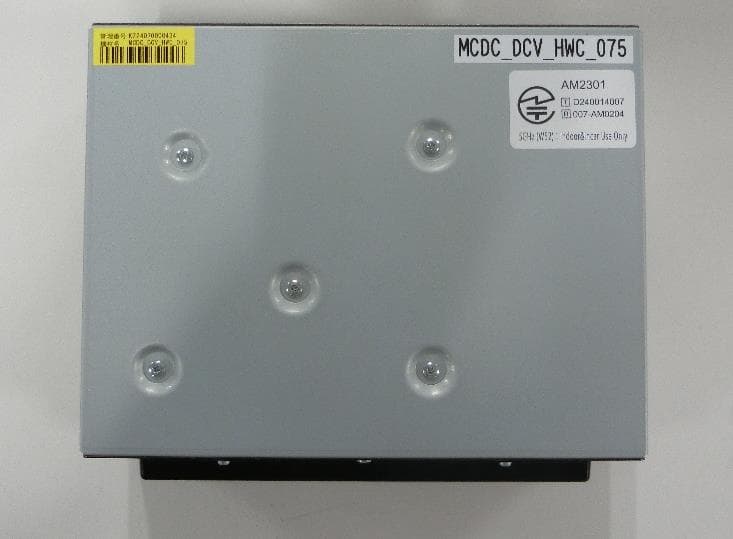
ACJ932AM2301
Jan 29, 2025Car AV Control Unit for CDC
Equipment Class
DTS - Digital Transmission SystemACJ96NKX-TGEA60B
Aug 13, 2024DECT Handset
Equipment Class
PUE - Part 15 Unlicensed PCS portable Tx held to earACJ96NKX-TGE630B
Aug 12, 2024DECT Base Unit
Equipment Class
PUB - Part 15 Unlicensed PCS Base Station