ACJ9TGWW11ATD-CDMA PCI Express Mini Module
Panasonic Corporation of North America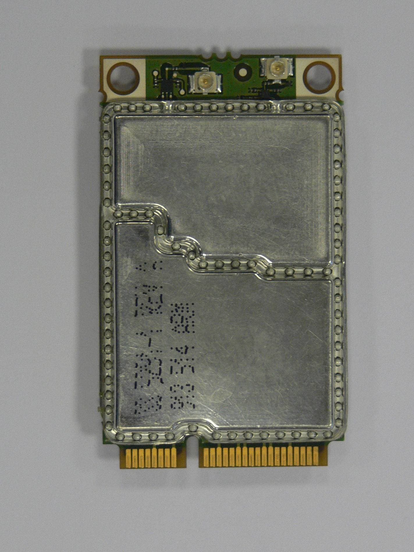
Click to zoom
Application Details
- Equipment Class
- TNB - Licensed Non-Broadcast Station Transmitter
- Date of Grant
- Feb 22, 2012
- Application Purpose
- Original Equipment
- Date of Application
- Feb 08, 2012
- Equipment Note
- TD-CDMA PCI Express Mini Module
- Frequency Range
- 2501.40000000 - 2684.60000000
- Country
- United States
Documents & Files
Document Text
Text extracted from the exhibit documents filed with the FCC. Open a document above to read the original.
Users Manual
Contents Getting Started Introduction .................................................................2 Read Me First .............................................................3 (Precautions) Description of Parts ....................................................9 Preparation ...............................................................11 First-time Operation ..................................................12 OPERATING INSTRUCTIONS Personal Computer Model No. CF-H2 series Useful Information On-screen Manual ....................................................16 Handling and Maintenance .......................................17 Reinstalling Software ................................................19 Troubleshooting Troubleshooting (Basic) ............................................21 Appendix LIMITED USE LICENSE AGREEMENT ...................25 Specifications ...........................................................27 LIMITED WARRANTY ..............................................30 Please read these instructions carefully before using this product, and save this manual for future use. For further information about the computer, you can refer to the on-screen manual. To access the on-screen manual è page 16 “On-screen Manual” Getting Started Useful Information Troubleshooting Appendix 2 Getting Started Introduction Thank you for purchasing this Panasonic product. For optimum performance and safety, please read these instructions carefully. In these instructions, the names are referred as follows. l Genuine “Windows ® 7 Professional” as “Windows” or “Windows 7” l Genuine “Microsoft ® Windows ® XP Tablet PC Edition Service Pack 3” as “Windows” or “Windows XP” n Terms and illustrations in these instructions è : Page in these Operating Instructions or in the Reference Manual. : Reference to the on-screen manuals. CAUTION : Conditions that may result in minor or moderate injury. NOTE : Useful and helpful information. Click : Touch the screen with the digitizer pen. Right-click : Touch and hold with the digitizer pen, or press and hold the right button, and then touch the object. (Start) - [All Programs] : Click (Start), and then click [All Programs]. [start] - [All Programs] : Click [start], and then click [All Programs]. You may need to double-click in some cases. <Only when connected to Cradle and keyboard> : Press [] (Enter) key. Ctrl + F7 : Press and hold Ctrl key, and then press F7 key. l The display of the key may be different from this manual according to the keyboard used. (e.g. “Delete” instead of “Del”) <For flash memory model> Read the term “hard disk” as “flash memory” whenever it appears in this manual. l Some illustrations are simplified to help your understanding and may look different from the actual unit. l If you do not log on as an administrator, you cannot use some functions or cannot display some screens. l Refer for the latest information about optional products to the catalogs, etc. n Disclaimer Computer specifications and manuals are subject to change without notice. Panasonic Corporation assumes no liability for damage incurred directly or indirectly from errors, omissions or discrepancies between the computer and the manuals. n Trademarks Microsoft ® , Windows ® and the Windows logo are registered trademarks of Microsoft Corporation of the United States and/or other countries. Intel, Core, Centrino and PROSet are either registered trademarks or trademarks of Intel Corporation. Adobe, the Adobe logo and Adobe Reader are either registered trademarks or trademarks of Adobe Systems Incorporated in the United States and/or other countries. Computrace ® is a registered trademark of Absolute ® Software Corp. Bluetooth™ is a trademark owned by Bluetooth SIG, Inc., U.S.A. and licensed to Panasonic Corporation. Names of products, brands, etc., appearing in this manual are trademarks or registered trademarks of their respective own companies. 3 Getting Started Federal Communications Commission Radio Frequency Interference Statement Note: This equipment has been tested and found to comply with the limits for a Class B digital device, pursuant to Part 15 of the FCC Rules. These limits are designed to provide reasonable protection against harmful interference in a residential installation. This equipment generates, uses and can radiate radio frequency energy and, if not installed and used in accordance with the instructions, may cause harmful interference to radio communications. However, there is no guarantee that interference will not occur in a particular installation. If this equipment does cause harmful interference to radio or television reception, which can be determined by turning the equipment off and on, the user is encouraged to try to correct the interference by one or more of the following measures: l Reorient or relocate the receiving antenna. l Increase the separation between the equipment and receiver. l Connect the equipment into an outlet on a circuit different from that to which the receiver is connected. l Consult the Panasonic Service Center or an experienced radio/TV technician for help. Warning To assure continued compliance, use only shielded interface cables when connecting to a computer or peripheral. Also, any changes or modifications not expressly approved by the party responsible for compliance could void the user’s authority to operate this equipment. This device complies with Part 15 of the FCC Rules. Operation is subject to the following two conditions: (1) This device may not cause harmful interference, and (2) This device must accept any interference received, including interference that may cause undesired operation. FCC RF Exposure Warning: <Only for model with wireless LAN/wireless WAN/ Bluetooth> l This equipment complies with FCC radiation exposure limits set forth for an uncontrolled environment. l This equipment has been approved for portable operation, and does not require any minimum spacing be provided between antennas and all…
Text truncated - open the document above for the full version.
Users Manual
OEM PCI Express Mini Module Integration OEM PCI Express Mini Module Integration Guide V01.02 4 th March 2009 IPWireless Proprietary and Confidential Page 1 of 10 Subject to Non Disclosure Agreement OEM PCI Express Mini Module Integration 4 th March 2009 IPWireless Proprietary and Confidential Page 2 of 10 Subject to Non Disclosure Agreement Contents 1 General ................................................................................................................ 3 1.1 Approvals and Dates ............................................................................................................... 3 1.2 Change Record ....................................................................................................................... 3 1.3 Acronyms ................................................................................................................................ 4 1.4 External References ................................................................................................................ 4 2 Introduction .......................................................................................................... 5 2.1 Scope of Document ................................................................................................................. 5 2.2 Overview of Module ................................................................................................................ 5 3 Module Connections ............................................................................................ 6 3.1 PCI Express Mini Interface (J1) .............................................................................................. 6 3.1.1 Universal Serial Bus ........................................................................................................ 6 3.1.2 SIM Interface ................................................................................................................... 6 3.2 Media Independent Interface (J4) ........................................................................................... 6 3.3 RF Connections ...................................................................................................................... 7 3.4 DC Power ................................................................................................................................ 7 4 Mechanical .......................................................................................................... 8 4.1 Thermal Management ............................................................................................................. 8 5 Regulatory Information ........................................................................................ 9 5.1 Compliance with FCC Rules and Regulations ........................................................................ 9 5.2 Exposure to Radio Frequency Signals .................................................................................... 9 6 Annex 1: PCI Express Mini Edge Connector Pinout .......................................... 10 Figures Figure 1: MII Interface J4 ........................................................................................................................ 6 Figure 2: RF Connections ....................................................................................................................... 7 Figure 3: PEM Module ............................................................................................................................ 8 OEM PCI Express Mini Module Integration 4 th March 2009 IPWireless Proprietary and Confidential Page 3 of 10 Subject to Non Disclosure Agreement 1 General 1.1 Approvals and Dates Approval Date W. J. Jones 1.2 Change Record Date Version Author Reason For Change Issue 20/08/2008 01.00 PFW New Document. 23/10/2008 01.01 PFW Additional details added. 04/03/2009 01.02 PFW Updated PEM Mechanical drawing. OEM PCI Express Mini Module Integration 4 th March 2009 IPWireless Proprietary and Confidential Page 4 of 10 Subject to Non Disclosure Agreement 1.3 Acronyms Term Definition MPE Maximum Permissible Exposure OEM Original Equipment Manufacturer PCIe PCI Express PCI SIG PCI Special Interest Group PEM PCI Express Mini SIM Subscriber Identity Module TDD Time Division Duplex UMTS Universal Mobile Telephone System USB Universal Serial Bus 1.4 External References Ref () Number Title 1 FCC Part 27 Miscellaneous Wireless Communications Service 2 PCI SIG PCI Express Base Specification Revision 2.0 3 PCI SIG Card Electromechanical Specification Revision 2.0 4 - PEM + Adapter Thermal Specification Revision 1.0 Note: Where a reference is undated, the latest version applies unless a specific revision is defined. OEM PCI Express Mini Module Integration 4 th March 2009 IPWireless Proprietary and Confidential Page 5 of 10 Subject to Non Disclosure Agreement 2 Introduction This document describes the method of integrating the IPWireless PCI Express Mini module into an OEM product. 2.1 Scope of Document This document applies to the IPWireless PCI Express Mini module only. 2.2 Overview of Module The IPWireless PCI Express Mini module provides a complete UMTS TDD wireless modem solution and only requires to be inserted in a PCI Express Mini compliant interface and connection of external antennas. The module is designed to minimise the time and resource required to integrate. OEM PCI Express Mini Module Integration 3 Module Connections 3.1 PCI Express Mini Interface (J1) The IPWireless PCI Express Mini module is provided with a 52 pin edge connector for connection to the external application. This connection supports the following interface types and these are described below. The pinout is shown in Annex 1. 3.1.1 Universal Serial Bus The PCI Express edge connector provides a USB 2.0 interface, this interface supports low speed (1.5Mbps), full speed (12Mbps) and High speed (480Mbps) operation. 3.1.2 SIM Interface The PCI Express edge connect…
Text truncated - open the document above for the full version.
Cover Letter(s)
Applicant/Grantee Panasonic Corporation of North America FCC ID: ACJ9TGWW11A Section 15.212 Modular Transmitters Request for Modular Approval Request for Limited Modular Approval Requirements EUT Conditions Comply (Y/N) Single Modular Approval Requirements 1 The radio elements of the modular transmitter must have their own shielding. The physical crystal and tuning capacitors may be located external to the shielded radio elements. The module has its own shielding and does not rely upon any shielding that maybe introduced as a result of integrating the module into a final product. Y 2 The modular transmitter must have buffered modulation/data inputs (if such inputs are provided) to ensure that the module will comply with Part 15 requirements under conditions of excessive data rates or over-modulation. The module provides a USB interface, this interface is digital and therefore does not allow excessive data rates or over-modulation to occur. Y 3 The modular transmitter must have its own power supply regulation. The module has on-board power conversion from the primary supply and is therefore not reliant on any power conversion from the host equipment. Y 4 The modular transmitter must comply with the antenna and transmission system requirements of Sections 15.203, 15.204(b) and 15.204(c). The antenna must either be permanently attached or employ a “unique” antenna coupler (at all connections between the module and the antenna, including the cable). The “professional installation” provision of Section 15.203 is not applicable to modules but can apply to limited modular approvals under paragraph (b) of this section. The module is not supplied with antennae and the antennae connectors provided on the pcb are considered unique connectors. Y 5 The modular transmitter must be tested in a stand- alone configuration, i.e., the module must not be inside another device during testing for compliance with Part 15 requirements. Unless the transmitter module will be battery powered, it must comply with the AC line conducted requirements found in Section 15.207. AC or DC power lines and data input/output lines connected to the module must not contain ferrites, unless they will be marketed with the module (see Section 15.27(a)). The length of these lines shall be the length typical of actual use or, if that length is unknown, at least 10 centimeters to insure that there is no coupling between the case of the module and supporting equipment. Any accessories, peripherals, or support equipment connected to the module during testing shall be unmodified and commercially available (see Section 15.31(i)). The module has been tested with installed in Panasonic Tablet PC CF- H2. N 6 The modular transmitter must be equipped with either a permanently affixed label or must be capable of electronically displaying its FCC identification number. The proposed FCC ID label format is to be placed on the module. If FCC ID is not visible when the module is installed into the system, Y (A) If using a permanently affixed label, the modular transmitter must be labeled with its own FCC identification number, and, if the FCC identification number is not visible when the module is installed inside another device, then the outside of the device into which the module is installed must also display a label referring to the enclosed module. This exterior label can use wording such as the following: “Contains Transmitter Module FCC ID: XYZMODEL1” or “Contains FCC ID: XYZMODEL1.” Any similar wording that expresses the same meaning may be used. The Grantee may either provide such a label, an example of which must be included in the application for equipment authorization, or, must provide adequate instructions along with the module which explain this requirement. In the latter case, a copy of these instructions must be included in the application for equipment authorization. (B) If the modular transmitter uses an electronic display of the FCC identification number, the information must be readily accessible and visible on the modular transmitter or on the device in which it is installed. If the module is installed inside another device, then the outside of the device into which the module is installed must display a label referring to the enclosed module. This exterior label can use wording such as the following: “Contains FCC certified transmitter module(s).” Any similar wording that expresses the same meaning may be used. The user manual must include instructions on how to access the electronic display. A copy of these instructions must be included in the application for equipment authorization. “Contains FCC ID: ACJ9TGWW11A” shall be placed on the outside of final host system. 7 The modular transmitter must comply with any specific rules or operating requirements that ordinarily apply to a complete transmitter and the manufacturer must provide adequate instructions along with the module to explain any such requirements. A copy of these instructions must be included in the application for equipment authorization. The integration instructions have been provided with this application. Y 8 The modular transmitter must comply with any applicable RF exposure requirements in its final configuration. The device complies with RF exposure compliance requirement. Y A limited modular approval may be granted for single or split modular transmitters that do not comply with all of the above requirements, e.g., shielding, minimum signaling amplitude, buffered modulation/data inputs, or power supply regulation, if the manufacturer can demonstrate by alternative means in the application for equipment authorization that the modular transmitter meets all the applicable Part 15 requirements under the operating conditions in which the transmitter will be used. Limited modular approval also may be granted in those instances where compliance with RF exposure rules is demonstrated only for particular product configurations. The applicant for certification must…
Text truncated - open the document above for the full version.
Cover Letter(s)
Panasonic Corporation of North America One Panasonic Way 4B-8 Secaucus, NJ 07094 Tel: 201-348-7758 / Fax: 201-392-4564 [email protected] RICHARD MULLEN Group Manager Product Safety and Compliance Division Agent Authorization Letter November 8, 2011 ITP-11-F030 UL CCS Certification Division 47173 Benicia Street Fremont, CA 94538, USA Re: Original Application TD-CDMA PCI Express Mini Module for Limited Modular Approval Panasonic TD-CDMA PCI Express Mini Module, Model WW11A / FCC ID: ACJ9TGWW11A Installation within Panasonic Personal Computer Model CF-H2mk1 To whom it may concern: The undersigned hereby authorizes Ms. Aliza Zaffar of Compliance Engineering Services, Inc., d.b.a. UL CCS and hereafter referred to as UL CCS, to act on our behalf in all manners relating to application for equipment authorization, including signing of all documents relating to these matters. Any and all acts carried out by Ms. Aliza Zaffar of UL CCS on our behalf shall have the same effect as acts of our own. The undersigned hereby certify that I am not subject to a denial of federal benefits, that includes FCC benefits, pursuant to Section 5301 of the Anti-Drug Abuse Act of 1988, 21 U.S.C. 853(a). Further, no party, as defined in 47 CFR 1.2002(b), to the application is subject to denial of federal benefits, that includes FCC benefits. This authorization is valid for one year period from the date of this letter. This application for the subject equipment has not been submitted to another TCB for certification In authorizing UL CCS as our agent, we still recognize that we are responsible to: a) Comply with the relevant provisions of the certification program; b) Make all necessary arrangements for the conduct of the evaluation, including provision for examining documentation and access to all areas, records (including internal audit reports) and personnel for the purposes of evaluation (e.g. testing, inspection, assessment, surveillance, reassessment) and resolution of complaints; c) Make claims regarding certification only in respect of the scope for which certification has been granted; d) Do not use our product certification in such a manner as to bring the Certification Division into disrepute and not make any statement regarding our product certification which the Certification Division may consider misleading or unauthorized; e) Upon suspension or cancellation of certification, discontinue use of all advertising matter that contains any reference thereto and return any certification documents as required by the Certification Division; f) Use certification only to indicate the products are certified as being in conformity with specified standards; g) Endeavor to ensure that no certificate or report nor any part thereof is used in a misleading manner; h) Ensure that any reference to our product certification in communication media such as documents, brochures or advertising, complies with the requirements of the Certification Division; Panasonic Corporation of North America One Panasonic Way 4B-8 Secaucus, NJ 07094 Tel: 201-348-7758 / Fax: 201-392-4564 [email protected] RICHARD MULLEN Group Manager Product Safety and Compliance Division November 8, 2011 ITP-11-F030 i) Keep a record of all complaints made known to the us relating to the product’s compliance with requirements of the relevant standard and to make these records available to the Certification Division when requested; j) Take appropriate action with respect to such complaints and any deficiencies found in products or services that affect compliance with the requirements for certification; k) Document the actions taken. Sincerely yours, Richard Mullen Richard Mullen Group Manager Product Safety & Compliance Division
RF Exposure Info
Date: 10/27/2011 Test Laboratory: UL CCS SAR Lab C 20111027_ELI-B_SystemPerformanceCheck-D2600V2 SN 1036 Communication System: CW; Frequency: 2600 MHz;Duty Cycle: 1:1 Medium parameters used: f = 2600 MHz; σ = 2.097 mho/m; ε r = 52.963; ρ = 1000 kg/m 3 Phantom section: Flat Section Room Ambient Temperature: 24.0 deg. C; Liquid Temperature: 23.0 deg. C DASY5 Configuration: - Area Scan setting - Find Secondary Maximum Within: 2.0 dB and with a peak SAR value greater than 0.0012W/kg - Probe: EX3DV4 - SN3772; ConvF(6.3, 6.3, 6.3); Calibrated: 5/3/2011 - Sensor-Surface: 2.5mm (Mechanical Surface Detection) - Electronics: DAE4 Sn1239; Calibrated: 10/18/2011 - Phantom: ELI v4.0 (B); Type: QDOVA001BB; Serial: 1121 - Measurement SW: DASY52, Version 52.6 (2);SEMCAD X Version 14.4.5 (3634) Body/Pin=100 mW/Area Scan (61x61x1): Measurement grid: dx=15mm, dy=15mm Maximum value of SAR (interpolated) = 8.309 mW/g Body/Pin=100 mW/Zoom Scan (7x7x7)/Cube 0: Measurement grid: dx=5mm, dy=5mm, dz=5mm Reference Value = 60.886 V/m; Power Drift = -0.10 dB Peak SAR (extrapolated) = 12.490 W/kg SAR(1 g) = 5.69 mW/g; SAR(10 g) = 2.5 mW/g Maximum value of SAR (measured) = 8.300 mW/g 0 dB = 8.300mW/g Date: 10/27/2011 Test Laboratory: UL CCS SAR Lab C 20111027_ELI-B_SystemPerformanceCheck-D2600V2 SN 1036 Communication System: CW; Frequency: 2600 MHz;Duty Cycle: 1:1 Body/Pin=100 mW/Z Scan (1x1x21): Measurement grid: dx=20mm, dy=20mm, dz=5mm Maximum value of SAR (measured) = 7.566 mW/g Date: 10/28/2011 Test Laboratory: UL CCS SAR Lab C 20111028_ELI-B_SystemPerformanceCheck-D2600V2 SN 1036 Communication System: CW; Frequency: 2600 MHz;Duty Cycle: 1:1 Medium parameters used: f = 2600 MHz; σ = 2.161 mho/m; ε r = 52.399; ρ = 1000 kg/m 3 Phantom section: Flat Section Room Ambient Temperature: 24.0 deg. C; Liquid Temperature: 23.0 deg. C DASY5 Configuration: - Area Scan setting - Find Secondary Maximum Within: 2.0 dB and with a peak SAR value greater than 0.0012W/kg - Probe: EX3DV4 - SN3772; ConvF(6.3, 6.3, 6.3); Calibrated: 5/3/2011 - Sensor-Surface: 2.5mm (Mechanical Surface Detection) - Electronics: DAE4 Sn1239; Calibrated: 10/18/2011 - Phantom: ELI v4.0 (B); Type: QDOVA001BB; Serial: 1121 - Measurement SW: DASY52, Version 52.6 (2);SEMCAD X Version 14.4.5 (3634) Body/Pin=100 mW/Area Scan (61x61x1): Measurement grid: dx=15mm, dy=15mm Maximum value of SAR (interpolated) = 8.317 mW/g Body/Pin=100 mW/Zoom Scan (7x7x7)/Cube 0: Measurement grid: dx=5mm, dy=5mm, dz=5mm Reference Value = 61.836 V/m; Power Drift = -0.02 dB Peak SAR (extrapolated) = 12.731 W/kg SAR(1 g) = 5.86 mW/g; SAR(10 g) = 2.59 mW/g Maximum value of SAR (measured) = 8.488 mW/g 0 dB = 8.490mW/g Date: 10/28/2011 Test Laboratory: UL CCS SAR Lab C 20111028_ELI-B_SystemPerformanceCheck-D2600V2 SN 1036 Communication System: CW; Frequency: 2600 MHz;Duty Cycle: 1:1 Body/Pin=100 mW/Z Scan (1x1x21): Measurement grid: dx=20mm, dy=20mm, dz=5mm Maximum value of SAR (measured) = 8.198 mW/g Date: 10/29/2011 Test Laboratory: UL CCS SAR Lab C 20111029_ELI-B_SystemPerformanceCheck-D2600V2 SN 1036 Communication System: CW; Frequency: 2600 MHz;Duty Cycle: 1:1 Medium parameters used: f = 2600 MHz; σ = 2.098 mho/m; ε r = 52.469; ρ = 1000 kg/m 3 Phantom section: Flat Section Room Ambient Temperature: 24.0 deg. C; Liquid Temperature: 23.0 deg. C DASY5 Configuration: - Area Scan setting - Find Secondary Maximum Within: 2.0 dB and with a peak SAR value greater than 0.0012W/kg - Probe: EX3DV4 - SN3772; ConvF(6.3, 6.3, 6.3); Calibrated: 5/3/2011 - Sensor-Surface: 2.5mm (Mechanical Surface Detection) - Electronics: DAE4 Sn1239; Calibrated: 10/18/2011 - Phantom: ELI v4.0 (B); Type: QDOVA001BB; Serial: 1121 - Measurement SW: DASY52, Version 52.6 (2);SEMCAD X Version 14.4.5 (3634) Body/Pin=100 mW/Area Scan (61x61x1): Measurement grid: dx=15mm, dy=15mm Maximum value of SAR (interpolated) = 8.465 mW/g Body/Pin=100 mW/Zoom Scan (7x7x7)/Cube 0: Measurement grid: dx=5mm, dy=5mm, dz=5mm Reference Value = 63.825 V/m; Power Drift = 0.0089 dB Peak SAR (extrapolated) = 13.290 W/kg SAR(1 g) = 5.91 mW/g; SAR(10 g) = 2.56 mW/g Maximum value of SAR (measured) = 8.683 mW/g 0 dB = 8.680mW/g Date: 10/29/2011 Test Laboratory: UL CCS SAR Lab C 20111029_ELI-B_SystemPerformanceCheck-D2600V2 SN 1036 Communication System: CW; Frequency: 2600 MHz;Duty Cycle: 1:1 Body/Pin=100 mW/Z Scan (1x1x21): Measurement grid: dx=20mm, dy=20mm, dz=5mm Maximum value of SAR (measured) = 8.463 mW/g Date: 10/31/2011 Test Laboratory: UL CCS SAR Lab C 20111031_ELI-B_SystemPerformanceCheck-D2600V2 SN 1036 Communication System: CW; Frequency: 2600 MHz;Duty Cycle: 1:1 Medium parameters used: f = 2600 MHz; σ = 2.17 mho/m; ε r = 52.787; ρ = 1000 kg/m 3 Phantom section: Flat Section Room Ambient Temperature: 24.0 deg. C; Liquid Temperature: 23.0 deg. C DASY5 Configuration: - Area Scan setting - Find Secondary Maximum Within: 2.0 dB and with a peak SAR value greater than 0.0012W/kg - Probe: EX3DV4 - SN3772; ConvF(6.3, 6.3, 6.3); Calibrated: 5/3/2011 - Sensor-Surface: 2.5mm (Mechanical Surface Detection) - Electronics: DAE4 Sn1239; Calibrated: 10/18/2011 - Phantom: ELI v4.0 (B); Type: QDOVA001BB; Serial: 1121 - Measurement SW: DASY52, Version 52.6 (2);SEMCAD X Version 14.4.5 (3634) Body/Pin=100 mW/Area Scan (61x61x1): Measurement grid: dx=15mm, dy=15mm Maximum value of SAR (interpolated) = 8.485 mW/g Body/Pin=100 mW/Zoom Scan (7x7x7)/Cube 0: Measurement grid: dx=5mm, dy=5mm, dz=5mm Reference Value = 61.639 V/m; Power Drift = -0.03 dB Peak SAR (extrapolated) = 12.856 W/kg SAR(1 g) = 5.91 mW/g; SAR(10 g) = 2.61 mW/g Maximum value of SAR (measured) = 8.512 mW/g 0 dB = 8.510mW/g Date: 10/31/2011 Test Laboratory: UL CCS SAR Lab C 20111031_ELI-B_SystemPerformanceCheck-D2600V2 SN 1036 Communication System: CW; Frequency: 2600 MHz;Duty Cycle: 1:1 Body/Pin=100 mW/Z Scan (1x1x21): Measurement grid: dx=20mm, dy=20mm, dz=5mm Maximum value of SAR (measured) = 8.122 mW/g Date: 1/5/2012 Test Laboratory: UL CCS SAR Lab C 2012 01 05_SystemPerformanceCheck-D2600V…
Text truncated - open the document above for the full version.
RF Exposure Info
Date: 10/27/2011 Test Laboratory: UL CCS SAR Lab C TD-CDMA 2.6GHz Band_Body_Primary Portrait Communication System: TD-CDMA; Frequency: 2593 MHz;Duty Cycle: 1:3.0 Medium parameters used (interpolated): f = 2593 MHz; σ = 2.087 mho/m; ε r = 52.988; ρ = 1000 kg/m 3 Phantom section: Flat Section Room Ambient Temperature: 24.0 deg. C; Liquid Temperature: 23.0 deg. C DASY5 Configuration: - Area Scan setting - Find Secondary Maximum Within: 2.0 dB and with a peak SAR value greater than 0.0012W/kg - Probe: EX3DV4 - SN3772; ConvF(6.3, 6.3, 6.3); Calibrated: 5/3/2011 - Sensor-Surface: 2.5mm (Mechanical Surface Detection) - Electronics: DAE4 Sn1239; Calibrated: 10/18/2011 - Phantom: ELI v4.0 (B); Type: QDOVA001BB; Serial: 1121 - Measurement SW: DASY52, Version 52.6 (2);SEMCAD X Version 14.4.5 (3634) QPSK_BW-10MHz_Mid-Ch/Area Scan (81x101x1): Measurement grid: dx=15mm, dy=15mm Info: Interpolated medium parameters used for SAR evaluation. Maximum value of SAR (interpolated) = 0.210 mW/g QPSK_BW-10MHz_Mid-Ch/Zoom Scan (5x5x7)/Cube 0: Measurement grid: dx=8mm, dy=8mm, dz=5mm Reference Value = 9.126 V/m; Power Drift = 0.04 dB Peak SAR (extrapolated) = 0.271 W/kg SAR(1 g) = 0.117 mW/g; SAR(10 g) = 0.063 mW/g Info: Interpolated medium parameters used for SAR evaluation. Maximum value of SAR (measured) = 0.161 mW/g 0 dB = 0.160mW/g Date: 10/27/2011 Test Laboratory: UL CCS SAR Lab C TD-CDMA 2.6GHz Band_Body_Primary Portrait Communication System: TD-CDMA; Frequency: 2593 MHz;Duty Cycle: 1:3.0 QPSK_BW-10MHz_Mid-Ch/Z Scan (1x1x21): Measurement grid: dx=20mm, dy=20mm, dz=5mm Info: Interpolated medium parameters used for SAR evaluation. Maximum value of SAR (measured) = 0.174 mW/g Date: 10/27/2011 Test Laboratory: UL CCS SAR Lab C TD-CDMA 2.6GHz Band_Body_Primary Portrait Communication System: TD-CDMA; Frequency: 2593 MHz;Duty Cycle: 1:3.0 Medium parameters used (interpolated): f = 2593 MHz; σ = 2.087 mho/m; ε r = 52.988; ρ = 1000 kg/m 3 Phantom section: Flat Section Room Ambient Temperature: 24.0 deg. C; Liquid Temperature: 23.0 deg. C DASY5 Configuration: - Area Scan setting - Find Secondary Maximum Within: 2.0 dB and with a peak SAR value greater than 0.0012W/kg - Probe: EX3DV4 - SN3772; ConvF(6.3, 6.3, 6.3); Calibrated: 5/3/2011 - S…
Text truncated - open the document above for the full version.
Contact Information
Applicant
Ben Botros(Project Manager)
Technical Contact
Compliance Certification ServicesThu Chan
[email protected](510)771-1000
47173 Benicia Street · Fremont · United States
Test Firm
Compliance Certification Services (UL CCS)Barbara Judge
Technical Specifications
| # | Rule Parts | Frequency Range | Power Output | Emission | Tolerance |
|---|---|---|---|---|---|
| 4 | 27 | 2.50 GHz - 2.68 GHz | 291.10 mW | 8M53G7D | 1 ppm |
Other Applications from Panasonic Corporation of North America
ACJ-EAH-A1000
Aug 19, 2026Digital Wireless Stereo Headphones
Equipment Class
DSS - Part 15 Spread Spectrum TransmitterACJ9TGFZVNF3G1
Jun 16, 2026Contactless Smart Card Reader
Equipment Class
DXX - Part 15 Low Power Communication Device Transmitter
ACJ932AM2301
Jan 29, 2025Car AV Control Unit for CDC
Equipment Class
DTS - Digital Transmission SystemACJ96NKX-TGEA60B
Aug 13, 2024DECT Handset
Equipment Class
PUE - Part 15 Unlicensed PCS portable Tx held to earACJ96NKX-TGE630B
Aug 12, 2024DECT Base Unit
Equipment Class
PUB - Part 15 Unlicensed PCS Base Station