ADMADP-611Digital Pen
Anoto Korea Corp.
Click to zoom
Application Details
- Equipment Class
- DTS - Digital Transmission System
- Date of Grant
- Sep 25, 2014
- Application Purpose
- Original Equipment
- Date of Application
- Sep 25, 2014
- Equipment Note
- Digital Pen
- Frequency Range
- 2402.00000000 - 2480.00000000
- Company
- Anoto Korea Corp.
- Country
- South Korea
Documents & Files
Document Text
Text extracted from the exhibit documents filed with the FCC. Open a document above to read the original.
Users Manual
How to use the Android application Function LED Mode User can do Bluetooth pairing with simple steps once the pen already registered as bluetooth device How to install the Android app. Search the app. named PenHub using the keyword “ADP-611” in Google Play and please do wnload and install the PenHub. Supported OS version - The PenHub can work under Android OS ver. 3.0(Honey comb) to 4.4(Kitkat) with BLE H/W How to Bluetooth pairing(Registering) in Android mobile device. 1. Run the PenHub application 2. Put the ADP-611 to search mode by turn-o and turn-on again. 3. Click the option button4. Click the Pen connection button 5. Tab the “Pen connection(Auto)” 6. Select the ADP-611 9. Please turn o and on after Bluetooth pairing(Registering) 7. Input the PIN code as “0000”8. Done the pairing Check the connection between the pen and the Android mobile device. The green LED keeps tur n-on status when the pen is connected correctly User can write a pen to exclusive notes or can view the saved note on the Android mobile device 1. Top LED(RED)2. Top LED(GREEN) Transmission in real time : Real time transmission the written contents by the digital pen from exclusive notes to the Android mobile device or computer in real time. Transmission after saving : The digital pen can save the written contents when it is not paired in Bluetooth. NOTE) To save the written contents, the pen should keep the turn-on status when it is written but it is no problem to save when the pen is not paired with Bluetooth. 1. Top LED(RED) : Blinking : Warning the low battery or memory full Keep on : Warning the discharged battery level or pen working error 2. Top LED(GREEN) : Blinking : Transmission after saving / Keep on : Transmission in real time 1.Click the option button3. Select your device4. Message for success to connect between the pen and the Android mobile device. 2. Click the Pen connection butt on Function and Mode 11 11 11 01. Digital Pen 611 02. Starter Note A5 03. Micro USB Cable 04. Pen Cap 05. Re ll / Stylus 01. Do not disassemble or otherwise attempt to change the form of the Digital Pen 611. 02. Do not crush, puncture or shred the Digital Pen 611. 03. Do contact the C/S center when the Digital pen doesn’t work. 04. Do not insert any other writing thing except supplied re ll 05. The pen is not working under - turned o - exceeded from the operation degree - put hand or something over the front of the pen(optical sensor) 06. Do not choke down the pen cap or re ll. 07. Do pay attention not to get pierced by a re ll 08. Do not let the pen come in contact with liquids and do not dry with heater by force 09. Do not place the pen in or near a heat source. 10. Do use the pen in the condition of room temperature. 11. Do not use the chemicals such as alcohol to clean the pen. Do use a piece of soft cloth. 12. Do not use incompatible charger. Misuse or use of incompatible charging device could result in damage to the equipment and a possible risk of re, explosion, or leakage, leading to serious injuries, damages to your pen. * Wireless device encountered interference from other devices. * Don’t attempt to use the battery improperly or replace yourself – you may damage the battery, which could cause overheating and injury. * Do dispose of the battery in accordance with local regulations. Never dispose of battery in a re because it may explode. Model Weight Communication Operating angle External interface Size Battery Charging method ADP-611 30g BLE -20 ~ +40 degree Micro USB Cable for charging 165 x 12.4 x 14mm 165 mm Li-Polymer Standard USB charging Unpacking Specification Caution This device complies with Part 15 of the FCC Rules. Operation is subject to the following two conditions: (1) this device may not cause harmful interference, and (2) this device must accept any interference received, including interference that may cause undesired operation. CAUTION : Any Changes or modifications not expressly approved by the manufacturer could void the user's authority to operate the equipment. This equipment has been tested and found to comply with the limits for a Class B digital device, pursuant to part 15 of the FCC Rules. These limits are designed to provide reasonable protection against harmful interference in a residential installation. This equipment generates, uses and can radiate radio frequency energy and, if not installed and used in accordance with the instructions, may cause harmful interference to radio communications. However, there is no guarantee that interference will not occur in a particular installation. If this equipment does cause harmful interference to radio or television reception, which can be determined by turning the equipment off and on, the user is encouraged to try to correct the interference by one or more of the following measures: · Reorient or relocate the receiving antenna. · Increase the separation between the equipment and receiver. · Connect the equipment into an outlet on a circuit different from that to which the receiver is connected. · Consult the dealer or an experienced radio/TV technician for help.
External Photos
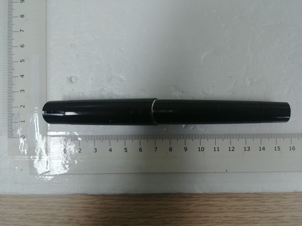
CTK Co., Ltd. (Ho-dong), 113, Yejik-ro, Cheoin-gu, Yongin-si, Gyeonggi-do, Korea Tel: +82-31-339-9970 Fax: +82-31-624-9501 www.e-ctk.com EUT External Photographs CTK Co., Ltd. (Ho-dong), 113, Yejik-ro, Cheoin-gu, Yongin-si, Gyeonggi-do, Korea Tel: +82-31-339-9970 Fax: +82-31-624-9501 www.e-ctk.com
ID Label/Location Info
CTK Co., Ltd. (Ho-dong), 113, Yejik-ro, Cheoin-gu, Yongin-si, Gyeonggi-do, Korea Tel: +82-31-339-9970 Fax: +82-31-624-9501 www.e-ctk.com Label and Location
Internal Photos
CTK Co., Ltd. (Ho-dong), 113, Yejik-ro, Cheoin-gu, Yongin-si, Gyeonggi-do, Korea Tel: +82-31-339-9970 Fax: +82-31-624-9501 www.e-ctk.com EUT Internal Photographs CTK Co., Ltd. (Ho-dong), 113, Yejik-ro, Cheoin-gu, Yongin-si, Gyeonggi-do, Korea Tel: +82-31-339-9970 Fax: +82-31-624-9501 www.e-ctk.com Main Board CTK Co., Ltd. (Ho-dong), 113, Yejik-ro, Cheoin-gu, Yongin-si, Gyeonggi-do, Korea Tel: +82-31-339-9970 Fax: +82-31-624-9501 www.e-ctk.com Sub Board CTK Co., Ltd. (Ho-dong), 113, Yejik-ro, Cheoin-gu, Yongin-si, Gyeonggi-do, Korea Tel: +82-31-339-9970 Fax: +82-31-624-9501 www.e-ctk.com Antenna Battery
Operational Description
Dielectric Chip Antenna - 1 - - Application Frequency Band[MHz] Bluetooth / WiFi/Zigbee 2400 ~ 2485 S-DMB2630 ~ 2655 Wibro 2300 ~ 2390 band1 : 2300 ~ 2327 band2 : 2331.5 ~ 2358.5 bnad3 : 2363 ~ 2390 Original Design Chip Antenna Data Sheet - P/N : SDBTPTR3015 - Dielectric Chip Antenna - 2 - ■ SDBTPTR3015 Dimension ParameterLWTABCDE Value[mm] 3.0 ±0.1 1.5 ±0.1 1.2 ±0.1 1.00.550.41.10.65 Unless Specified tolerances are ± 0.05 mm Dielectric Chip Antenna - 3 - ■ Antenna Marking System ◀S3 ①②③ ITEMDESCRIPTION ① Input Signal Input Signal ② Serial SDBTPTR3015 ③ Month ■ Antenna PAD Information 3 12 4 Via No Ground Region 1005 series 1005 series Ground Region 0.5mm feed line 123456 JanuaryFebruaryMarchAprilMayJune 789ABC JulyAugustSeptemberOctoberNovemberDecember ◀ S3 Dielectric Chip Antenna - 4 - ■ PCB Drawing Top View Case #1 <Default> 12 3 4 Case #2 12 3 4 Case #3 12 3 4 Case #4 12 3 4 Bottom View <Equivalent Circuit> Dielectric Chip Antenna - 5 - ■ Change of Antenna Position 3 1 2 4 Via No Ground Region 1005 series 1005 series Ground Region 0.5mm feed line ◀ S ○ Antenna Position Feeding Position LeftDown DownRight 2 4 3 1 Via No Ground Region 1005 series 1005 series Ground Region 0.5mm feed line ◀ S ○ Antenna Position Feeding Position LeftUp UpRight Antenna Position Feeding Position RightDown DownLeft 3 4 2 1 Via No Ground Region 1005 series 1005 series Ground Region 0.5mm feed line ◀ S ○ Antenna Position Feeding Position RightUp UpLeft 3 1 2 4 Via No Ground Region 1005 series 1005 series Ground Region 0.5mm feed line ◀ S ○ Dielectric Chip Antenna - 6 - ■ Matching Value Band (MHz) Matching Value (Default) Bluetooth / WiFi / Zigbee (2400 ~ 2485) Connector N/C Ant. 100pF 1.8pF 100 pF N/C S-DMB ( 2630 ~ 2655) Connector N/C Ant. 100pF 1.0pF 100 pF N/C Wibro (2300 ~ 2390) band1:2300~2327 band2:2331.5~2358.5 bnad3:2363~2390 Connector N/C Ant. 100pF 2.0pF 100 pF N/C Dielectric Chip Antenna - 7 - - 3D Passive Gain For Bluetooth / WiFi / Zigbee ■ Test Result for Ver 0.0 SWR & Smith chart3D Peak [dBi] Average [dBi] Efficiency [%] 2400MHz1.96-0.9780.18 2425MHz1.99-0.6685.92 2445MHz1.74-0.8582.42 2465MHz1.27-1.2575.12 2485MHz0.86-1.6468.59 ■ Radiation PatternVer 0.0 3D Passive Dielectric Chip Antenna - 8 - - 3D Passive Gain For S-DMB ■ Test Result for Ver 0.0 SWR & Smith chart3D Peak [dBi] Average [dBi] Efficiency [%] 2627MHz4.33-0.3891.80 2642MHz4.67-0.3692.06 2657MHz4.71-0.5688.02 ■ Radiation PatternVer 0.0 3D Passive Dielectric Chip Antenna - 9 - - 3D Passive Gain For Wibro ■ Test Result for Ver 0.0 SWR & Smith chart3D Peak [dBi] Average [dBi] Efficiency [%] 2300MHz2.51-0.8482.52 2322.5MHz2.68-0.7883.71 2345MHz3.15-0.4590.20 2367.5MHz3.02-0.7883.76 2390MHz3.09-0.8682.12 ■ Radiation PatternVer 0.0 3D Passive Dielectric Chip Antenna - 10 - ■ AutoCAD Drawing of Reference PCB Design for SDBTPTR3015 Product 41 2 3
RF Exposure Info
CTK Co., Ltd. (Ho-dong), 113, Yejik-ro, Cheoin-gu, Yongin-si, Gyeonggi-do, Korea Tel: +82-31-339-9970 Fax: +82-31-624-9501 www.e-ctk.com Page 1 of 2 RF EXPOSURE EVALUATION Applicant : Pen Generations, Inc. Applicant Address : 8th Fl.,Pangyotechnovalley SOLID Space, 220 Pangyoyeokro, Bundang-gu, Seongnam-si, Gyeonggi-do, Korea 463-400 Kind of Product : Digital Pen FCC ID : ADMADP-611 RF power : -4.751 dBm Peak Conducted Antenna type : Chip antenna Antenna Gain : 1.99 dBi Frequency Range : 2402 MHz - 2480 MHz Number of channels : 40 CH CTK Co., Ltd. (Ho-dong), 113, Yejik-ro, Cheoin-gu, Yongin-si, Gyeonggi-do, Korea Tel: +82-31-339-9970 Fax: +82-31-624-9501 www.e-ctk.com Page 2 of 2 ** MPE Calculations ** No Evaluation Required if power is below this threshold. (60/f(GHz) mW) Frequency (GHz) mW Lowest 2.402 24.98 Highest 2.480 24.19 The MPE calculation for this exposure is shown below. EIRP = P + G Where, P = Conducted output power (dBm) G = Power gain of the antenna (dBi) Measured Transmitter Output Power(Maximum : GFSK, CH 0) Output Power(dBm) Antenna gain (dBi) EIRP (dBm) EIRP (mW) -4.751 1.99 -2.761 0.530 Conclusion: No SAR evaluation required since Transmitter EIRP is below FCC threshold.
Test Report
CTK Co., Ltd. (Ho-dong), 113, Yejik-ro, Cheoin-gu, Yongin-si, Gyeonggi-do, Korea Tel: +82-31-339-9970 Fax: +82-31-624-9501 www.e-ctk.com Test Report No.: CTK-2014-01170 Date: 2014-09-25 Page 1 of 34 This Report shall not be reproduced except in full without the written approval of CTK Form No.: CTK-RF-EF-Part15 Subpart C(Rev.2) TEST REPORT According to : FCC 47CFR part 15 subpart C § 15.247 Test Report No. : CTK-2014-01170 Date of Issue : 2014-09-25 FCC ID : ADMADP-611 Model/Type No. : ADP-611 Kind of Product : Digital Pen Applicant : Pen Generations, Inc. Applicant Address : 8th Fl.,Pangyotechnovalley SOLID Space, 220 Pangyoyeokro Bundang-gu, Seongnam-si, Gyeonggi-do, Korea 463-400 Manufacturer : Pen Generations, Inc. Manufacturer Address : 8th Fl.,Pangyotechnovalley SOLID Space, 220 Pangyoyeokro Bundang-gu, Seongnam-si, Gyeonggi-do, Korea 463-400 Contact Person : Sang Nyeon Cho / Assistant Manager Telephone : +82–31-600-0840 Received Date : 2014-09-04 Test period : Start : 2014-09-19 End : 2014-09-24 Test Results : In Compliance Not in Compliance The test results presented in this report relate only to the object tested. Tested by Reviewed by Young-taek Lee Test Engineer Young-Joon, Park Technical Manager Date: 2014-09-25 Date: 2014-09-25 CTK Co., Ltd. (Ho-dong), 113, Yejik-ro, Cheoin-gu, Yongin-si, Gyeonggi-do, Korea Tel: +82-31-339-9970 Fax: +82-31-624-9501 www.e-ctk.com Test Report No.: CTK-2014-01170 Date: 2014-09-25 Page 2 of 34 This Report shall not be reproduced except in full without the written approval of CTK Form No.: CTK-RF-EF-Part15 Subpart C(Rev.2) REPORT REVISION HISTORY Date Revision Page No 2014-09-25 Issued (CTK-2014-01170) All This report shall not be reproduced except in full, without the written approval of CTK Co., Ltd. This document may be altered or revised by CTK Co., Ltd. personnel only, and shall be noted in the revision section of the document. Any alteration of this document not carried out by CTK Co., Ltd. will constitute fraud and shall nullify the document. CTK Co., Ltd. (Ho-dong), 113, Yejik-ro, Cheoin-gu, Yongin-si, Gyeonggi-do, Korea Tel: +82-31-339-9970 Fax: +82-31-624-9501 www.e-ctk.com Test Report No.: CTK-2014-01170 Date: 2014-09-25 Page 3 of 34 This Report shall not be reproduced except in full without the written approval of CTK Form No.: CTK-RF-EF-Part15 Subpart C(Rev.2) TABLE OF CONTENTS REPORT REVISION HISTORY ........................................................................................... 2 1.0 General Product Description ................................................................................ 4 1.1 Tested Frequency ............................................................................................... 4 1.2 Duty Cycle ........................................................................................................ 5 1.3 Model Differences .............................................................................................. 5 1.4 Device Modifications ........................................................................................... 5 1.5 Peripheral Devices ............................................................................................. 5 1.6 Calibration Details of Equipment Used for Measurement ......................................... 6 1.7 Test Facility ....................................................................................................... 6 1.8 Laboratory Accreditations and Listings .................................................................. 6 2.0 Summary of tests .............................................................................................. 7 2.1 Technical Characteristic Test ...................................................................................... 8 2.1.1 6dB Bandwidth ............................................................................................ 8 2.1.2 Maximum peak Conducted Output Power ...................................................... 11 2.1.3 Power Spectral Density ............................................................................... 14 2.1.4 Band - edge .............................................................................................. 17 2.1.5 Field Strength of Emissions ......................................................................... 22 2.1.6 AC Conducted Emissions ............................................................................. 31 APPENDIX A – Test Equipment Used For Tests ................................................................. 34 CTK Co., Ltd. (Ho-dong), 113, Yejik-ro, Cheoin-gu, Yongin-si, Gyeonggi-do, Korea Tel: +82-31-339-9970 Fax: +82-31-624-9501 www.e-ctk.com Test Report No.: CTK-2014-01170 Date: 2014-09-25 Page 4 of 34 This Report shall not be reproduced except in full without the written approval of CTK Form No.: CTK-RF-EF-Part15 Subpart C(Rev.2) 1.0 General Product Description Equipment model name : ADP-611 Serial number : Prototype EUT condition : Pre-production, not damaged Antenna type : Chip antenna Gain 1.99 dBi Frequency Range : 2402 MHz – 2480 MHz RF output power : -4.751 dBm Peak Conducted Number of channels : 40 Type of Modulation : GFSK (Bluetooth 4.0 - LE) Rated Channel spacing : 2 MHz Power Source : DC 3.7 V (Rechargeable Lithium Polymer Battery) 1.1 Tested Frequency LOW MID HIGH Frequency (MHz) 2402 2440 2480 CTK Co., Ltd. (Ho-dong), 113, Yejik-ro, Cheoin-gu, Yongin-si, Gyeonggi-do, Korea Tel: +82-31-339-9970 Fax: +82-31-624-9501 www.e-ctk.com Test Report No.: CTK-2014-01170 Date: 2014-09-25 Page 5 of 34 This Report shall not be reproduced except in full without the written approval of CTK Form No.: CTK-RF-EF-Part15 Subpart C(Rev.2) 1.2 Duty Cycle Duty Cycle 63.9 % 1.3 Model Differences Not applicable 1.4 Device Modifications The following modifications were necessary for compliance: Not applicable 1.5 Peripheral Devices Device Manufacturer Model No. Serial No. BLUETOOTH TESTER TESCOM TC-3000C 3000C000377 Notebook Compute…
Text truncated - open the document above for the full version.
Test Setup Photos
CTK Co., Ltd. (Ho-dong), 113, Yejik-ro, Cheoin-gu, Yongin-si, Gyeonggi-do, Korea Tel: +82-31-339-9970 Fax: +82-31-624-9501 www.e-ctk.com Test Setup Photographs and Configuration Conducted Voltage Emissions CTK Co., Ltd. (Ho-dong), 113, Yejik-ro, Cheoin-gu, Yongin-si, Gyeonggi-do, Korea Tel: +82-31-339-9970 Fax: +82-31-624-9501 www.e-ctk.com Radiated Electric Field Emissions CTK Co., Ltd. (Ho-dong), 113, Yejik-ro, Cheoin-gu, Yongin-si, Gyeonggi-do, Korea Tel: +82-31-339-9970 Fax: +82-31-624-9501 www.e-ctk.com
Contact Information
Applicant
Changhoon Shin(Assistant Research Engineer)
Test Firm
CTK Co., Ltd.Young-Joon Park
Technical Specifications
| # | Rule Parts | Frequency Range | Power Output |
|---|---|---|---|
| 1 | 15C | 2.40 GHz - 2.48 GHz | 300.00 µW |
Other Applications from Anoto Korea Corp.
ADM-ANDANTE
Jan 13, 2020Digital Pen
Equipment Class
DTS - Digital Transmission System