AMWUH302Wireless Cellular Digital Packet Data (CDPD) PC Ca
Uniden America Corporation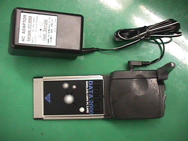
Click to zoom
Application Details
- Equipment Class
- TNB - Licensed Non-Broadcast Station Transmitter
- Date of Grant
- Nov 04, 1998
- Application Purpose
- Original Equipment
- Date of Application
- Aug 12, 1998
- Equipment Note
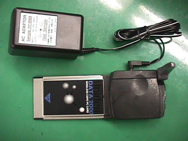
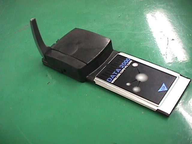
- Wireless Cellular Digital Packet Data (CDPD) PC Ca
- Frequency Range
- 824.00000000 - 849.00000000
- Company
- Uniden America Corporation
- Country
- United States
Documents & Files
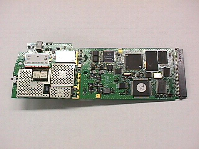
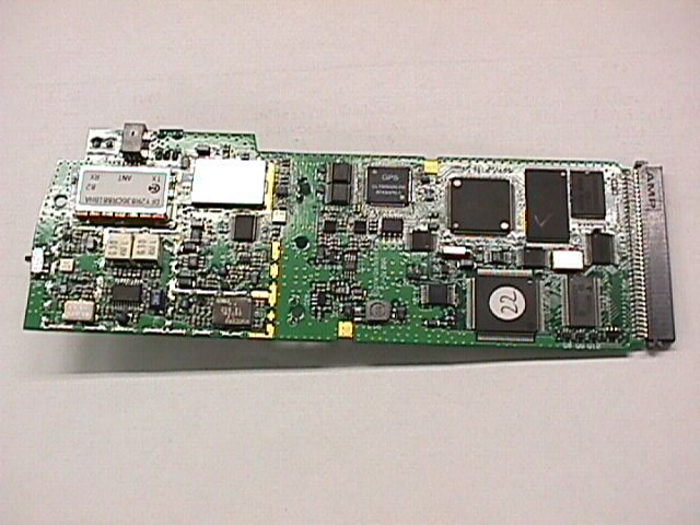
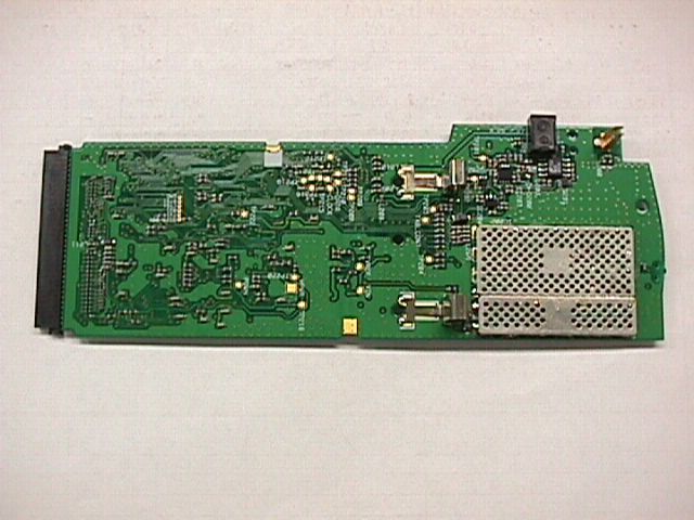
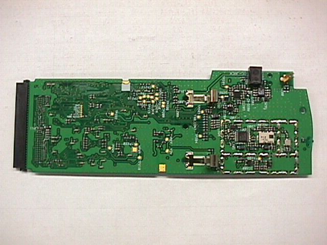
Document Text
Text extracted from the exhibit documents filed with the FCC. Open a document above to read the original.
Users Manual
s Uniden Data 2000 Wireless CDPD PC Card Uniden Data 2000 Operation & Programming Guide 1-1 1 Uniden Data 2000 Introduction 1.1 What is the Uniden Data 2000? The Uniden Data 2000 is a wireless CDPD PC Card which enables most vendors’ laptops, handheld computers, and Personal Digital Assistants with Type II PC Card slots to communicate with host-based applications such as web servers, intranet servers, databases, dispatch systems, and other host computer systems. The Uniden Data 2000 uses the Internet suite of protocols running over the CDPD (Cellular Digital Packet Data) system. The product is fully Windows compatible, supporting Windows 95, Windows NT, and Windows CE, and provides a Graphical User Interface (GUI) which offers the user simplified access to operational status and statistics, as well as the ability to configure, control, and mon- itor the performance of the device. The Uniden Data 2000’s compact size makes it an easily portable communications tool that can be stored conveniently in a briefcase or purse when not in use. 1.2 What is CDPD? CDPD or Cellular Digital Packet Data is a wireless, public access, packet data standard designed to operate over existing analog cellular phone systems. Since it is designed to use existing cellular phone sys- tems, CDPD provides a large coverage area, low service pricing, and fast transaction execution. CDPD’s primary benefit is quick, inexpen- sive, and efficient transmission of data packets over the existing cellular network. Additional benefits include built-in encryption for security (where applicable); a billing structure which charges for message size rather than on-line time (depending on individual service provider’s ser- vice plans); forward error correction methods that reduce the effects of noise and interference on the airlink; and availability. s Uniden Data 2000 Wireless CDPD PC Card 1-2 1.3 What is the PCMCIA Standard for PC Cards? Over the past several years, mobile computers have experienced explo- sive growth. While prices have fallen sharply, features are becoming more advanced and reliability has been greatly improved. One of the most notable features of today’s mobile computers is the PC Card slot. Over the last four years, the personal computer industry has rapidly adopted the PC Card slot feature, and today nearly 75 percent of laptops include a PC Card slot. This has been the driving force in the innovation and development of PC Card technology. In 1989, an international standards body and trade association was founded, called the PCMCIA (Personal Computer Memory Card Inter- national Association.). This organization was founded in order to estab- lish standards for Integrated Circuit cards and to promote interchangeability among mobile computers where ruggedness, low power, and small size are critical. Even though PCMCIA is a rather young technology, it has been quickly adopted by every major personal computer manufacturer in the world. Since it’s inception, PCMCIA has published a PC Card Standard which contains all of the physical, electrical and software specifications for PC Card technology. This standard is in a constant state of improvement by the PCMCIA technical committee. s Uniden Data 2000 Wireless CDPD PC Card Uniden Data 2000 Operation & Programming Guide 1-3 1.4 Product Highlights •Compatible with most vendors’ laptops, handheld computers and Personal Digital Assistants (PDAs) with PCMCIA Type II PC Card slots. •Windows compatible (Windows 95, Windows NT, and Win- dows CE.) •Graphical User Interface (GUI) provides simplified access to operational status and statistics, and allows the user to config- ure, control, and monitor the performance of the device. •AT command interface allows the user to query status and sta- tistics, change operational modes, and configure and control the device. •External antenna connector allows a high gain antenna to be substituted for maximum performance. •Full Duplex operation with CDPD System Specification Ver- sion 1.1. •Data transfer via SLIP or PPP to a connected host, using the PCMCIA interface. •Embedded TCP/UDP/IP stack from which an embedded appli- cation can achieve data transfer capability to the CDPD net- work. •Embedded network connectivity application, for testing end-to- end connectivity. •Maximum of 10 unicast Network Equipment Identifiers (NEIs) which can be stored and activated one at a time. •Onboard battery for operation independent of host. •External power option for desktop use. s Uniden Data 2000 Wireless CDPD PC Card 1-4 **need photo 1.5 Package Contents •Uniden Data 2000 Wireless CDPD PC Card: The physical module containing all of the electronic and other hardware ele- ments. (Includes the battery compartment, antenna and PCM- CIA interface connector.) The PC Board is protected by a clam shell structure made from a 2-piece plastic sub-frame, molded together with a stamped stainless steel cover. •Installation Diskette: **need info •Support Utilities Diskette: **need info •Uniden Data 2000 Operation and Programming Guide s Uniden Data 2000 Wireless CDPD PC Card Uniden Data 2000 Operation & Programming Guide 1-5 1.6 Optional Accessories •NiCd battery pack •NiCd battery charger •Antenna adapter (To allow use of high gain antenna.) s Uniden Data 2000 Wireless CDPD PC Card Uniden Data 2000 Operation & Programming Guide 2-1 2 Setting Up the Uniden Data 2000 This chapter explains how to set up the Uniden Data 2000 Wireless CDPD PC Card for operation with host terminals running Windows 95, Windows NT, and Windows CE. 2.1 Setup Preparation 2.1.1 Hardware Required for Uniden Data 2000 Set Up •A host terminal, (laptop, handheld computer, or Personal Digi- tal Assistant) •The Uniden Data 2000 Wireless CDPD PC Card. 2.1.2 Software Required for Uniden Data 2000 Set Up One of the following operating systems is required: •Windows 95 •Windows NT •Windows CE 2.1.3 Requesting Service Activation Before you can use the Uniden Data 2000, you must contact your local cellula…
Text truncated - open the document above for the full version.
Users Manual
FCC ID: AMWUH302 The following statement will be added to the Owner’s Manual on a “running change” basis. Until then, this statement will be added to the user’s documentation as an addendum sheet. Caution - Before operating this device, be sure to place the antenna in the vertical position. This will offer the best performance of your modem, and at the same time it will reduce the risk of possible exposure to electromagnetic radiation which is emanated from the antenna.
Users Manual
Caution - Before operating this device, be sure to place the antenna in the vertical position. This offers the best per- formance of your modem, and, at the same time, reduces the risk of possible exposure to electromagnetic radiation emanating from the antenna. The antenna must be maintained at least 4 inches (or 10 cm) from users and nearby persons to comply with FCC radiofrequency exposure limits (and to reduce the risk of RF radiation) when the DATA 2000 is in operation." 1-1What is the Uniden Data 2000? The Uniden Data 2000 is a wireless CDPD PC Card which enables most vendors’ laptops, handheld computers, and Personal Digital Assistants with Type II PC Card slots to communicate with host-based applications such as web servers, intranet servers, databases, dispatch systems, and other host computer systems. The Uniden Data 2000 uses the Internet suite of protocols running over the CDPD (Cellular Digital Packet Data) system. The product is fully Windows compatible, supporting Windows 95, Windows NT, and Windows CE, and provides a Graphical User Interface (GUI) which offers the user simplified access to operational status and statistics, as well as the ability to configure, control, and moni- tor the performance of the device. The Uniden Data 2000’s compact size makes it an easily portable communications tool that can be stored con- veniently in a briefcase or purse when not in use. sUniden Data 2000 Wireless CDPD PC Card Uniden Data 2000 Introduction 1 Uniden Data 2000 Operation & Programming Guide1-1 RAISE ANTENNA sUniden Data 2000 Wireless CDPD PC Card 1-2What is CDPD? CDPD or Cellular Digital Packet Data is a wireless, public access, pack- et data standard designed to operate over existing analog cellular phone systems. Since it is designed to use existing cellular phone sys- tems, CDPD provides a large coverage area, low service pricing, and fast transaction execution. CDPD’s primary benefit is quick, inexpen- sive, and efficient transmission of data packets over the existing cellu- lar network. Additional benefits include built-in encryption for security (where applicable); a billing structure which charges for message size rather than on-line time (depending on individual service provider’s service plans); forward error correction methods that reduce the effects of noise and interference on the airlink; and availability. 1.3What is the PCMCIA Standard for PC Cards? Over the past several years, mobile computers have experienced explosive growth. While prices have fallen sharply, features are becom- ing more advanced and reliability has been greatly improved. One of the most notable features of today’s mobile computers is the PC Card slot. Over the last four years, the personal computer industry has rapid- ly adopted the PC Card slot feature, and today nearly 75 percent of lap- tops include a PC Card slot. This has been the driving force in the innovation and development of PC Card technology. In 1989, an international standards body and trade association was founded, called the PCMCIA (Personal Computer Memory Card International Association.). This organization was founded in order to establish standards for Integrated Circuit cards and to promote inter- changeability among mobile computers where ruggedness, low power, and small size are critical. Even though PCMCIA is a rather young technology, it has been quickly adopted by every major personal computer manufacturer in the world. Since it’s inception, PCMCIA has published a PC Card Standard which contains all of the physical, electrical and software specifications for PC Card technology. This standard is in a constant state of improve- ment by the PCMCIA technical committee. 1-2 1.4Product Highlights lCompatible with most vendors’ laptops, handheld computers and Personal Digital Assistants (PDAs) with PCMCIA Type II PC Card slots. lWindows compatible (Windows 95, Windows NT, and Windows CE.) lGraphical User Interface (GUI) provides simplified access to operational status and statistics, and allows the user to config- ure, control, and monitor the performance of the device. lAT command interface allows the user to query status and sta- tistics, change operational modes, and configure and control the device. lExternal antenna connector allows a high gain antenna to be substituted for maximum performance. lFull Duplex operation with CDPD System Specification Version 1.1. lData transfer via SLIP or PPP to a connected host, using the PCMCIA interface. lEmbedded TCP/UDP/IP stack from which an embedded application can achieve data transfer capability to the CDPD network. lEmbedded network connectivity application, for testing end- to-end connectivity. lMaximum of 10 unicast Network Equipment Identifiers (NEIs) which can be stored and activated one at a time. lOnboard battery for operation independent of host. lExternal power option for desktop use. sUniden Data 2000 Wireless CDPD PC Card Uniden Data 2000 Operation & Programming Guide1-3 sUniden Data 2000 Wireless CDPD PC Card 1.5Package Contents lUniden Data 2000 Wireless CDPD PC Card:The physical module containing all of the electronic and other hardware elements. (Includes the battery compartment, antenna and PCMCIA interface connector.) The PC Board is protected by a clam shell structure made from a 2-piece plastic sub-frame, molded together with a stamped stainless steel cover. lInstallation Diskette:**need info lSupport Utilities Diskette: **need info lUniden Data 2000 Operation and Programming Guide 1.6Optional Accessories lNiCd battery pack lNiCd battery charger lAntenna adapter (To allow use of high gain antenna.) 1-4
Block Diagram
DuplexerPLL Threshold Control TX Chain I/Q Mod Sig Forward Sync Engine Reverse Sync Engine MCU/ ASIC Interface MCU Battery Management Memory Flash E 2 PROM SRAM TCVCXO Bit Timing AFC1 AFC2 Reed Solomon decoder BoB R_S Reed Solomon encoder EOB EOT Busy Idle μ Slot ck TX RESP ADD Data CS RD_N WR_N PCMCIA Connector Charging Path 32.768 KHz External Charger 2.30 4 MHz I RX Chain Lim Disc Filter Q PA_ON PA_RAMP PLL CONTROL RSSI Dual Port RAM PCMCIA Controller Battery Monitor ASIC Radio Module Baseband Module Battery Overall PC-Card Block Diagram
Operational Description
GENERAL INFORMATION General Information in accordance with the Federal Communications Commission Rules and Regulations, Volume II, Part 2. Section 2.983(a) Applicant: Uniden America Corporation Engineering Services Office 216 John Street, P.O. Box 580 Lake City, South Carolina 29560 Mr. James R. Haynes, Vice President Section 2.983(b) Equipment Identification: FCC ID: AMWUH302 MODEL : Data 2000 Section 2.983(c) Quantity: Quantity Production is planned. Section 2.983(d)(1) Emission Type: 28K8FXW Section 2.983(d)(2) Frequency Range: 824 - 849 MHz Section 2.983(d)(3) Operating Power: 600mW - 6 mW Section 2.983(d)(4) Maximum Power Rating: According to the section 22.904 of the FCC Rules. Section 2.983(d)(6) Solid State Devices: Refer to EXHIBIT-3 Section 2.983(d)(7) Circuit & Block Diagram: Refer to EXHIBIT-4 Section 2.983(d)(8) Instruction Manual: Refer to EXHIBIT-5 Section 2.983(d)(10)(11) Circuit Descriptions: Refer to EXHIBIT-2 Section 2.983(d)(12) Description of Digital Modulation Techniques: Not Applicable Section 2.983(f) Equipment Identification: Refer to EXHIBIT-8
Operational Description
System Design Document TemplateError! Reference source not found. 9900-0003 Version 1.0 SRC SRCSRC SRC PC Card System Design Document Document #6410-0003 Revision History RevisionIssue DateOriginatorDescription 1.14/30/97R. KumarFirst open project-wide release. - compiled from individual chapter documents provided by Jonathon, Rich, David Crandall, W. Rou, H. Eassie, N. Nguyen, K. Luu, Tri Le 1.25/7/97R. KumarUpdated RF chapter to include discrete external-to-asic DACs 1.3TBDR. KumarRelease for SRC inspection process Uniden San Diego Research and Development Center San Diego, California 92121 Copyright 1997 Uniden SRC, Inc. All rights reserved. 1. Introduction 1 Purpose This document describes the design approach of the Uniden CDPD PCMCIA Type II device design considerations code named PC-card. The Uniden CDPD PC-card shall comply with the CDPD (Cellular Digital Packet Data) Specification Release 1.1, 19 th January 1995. PC-card is intended to be a consumer product to allow an add-on wireless communication capability for laptop PC or PDA users. For this design to be suitably used with a portable computer, it is necessary to satisfy the PCMCIA type II mechanical form factor, and the low power consumption requirements. To facilitate the host computer control interface, it is also necessary for this device to satisfy the portable PC operating system (OS) environment, which is currently assumed to be Microsoft Windows PCMCIA interface data services. This design is based on the CDPD full duplex mode operation. Operationally, this product shall comply with CDPD system specifications mentioned above with all the advanced features such as Sleep Mode, Broadcast, Multicast and ZAP. 2 Scope This document is divided into 7 chapters. Chapter 1This introductory chapter. Chapter 2This chapter provides the system design and partitioning of the hardware components of the product. Chapter 3This chapter explains the system design and partitioning of the software components of the product. Chapter 4This chapter focuses on the mechanical system design of the product. Chapter 5This chapter provides a narrative description of operational states and detailed analysis of issues such as power consumption. Chapter 6This chapter describes the service and maintenance methodology designed into the product, both for production and field service. 3 Applicable Documents 1. Product XYZ Requirements Document, V1.0, 25-December, 1995 2. Product XYZ Design Specifications, V1.0, 26-Decemnber,1995 3. EIA 123 Interface Specifications 4 Open Issues Log << Any open issues in the system design are mentioned here..>> 2. Overview of the System 1 Functional Overviews .1 Hardware functional overview The physical dimensions and the power consumption requirements drive the system design concept into adopting a single MAC layer ASIC partitioned in such as a way that all non MAC protocol decision related processes are done in ASIC hardware. The main intent of the ASIC partition is to eliminate any computation intensive elements of the system from the MCU so that no DSP class processing power is needed. Furthermore, as power consumption is function of the system clock speed, an overall system clock speed of in the order of 2 Mhz is desirable. A dedicated PCMCIA controller will be used to interface with the host computer. A full duplex cellular transceiver will provided for the airlink interface. Figure 1.1 shows the overall block diagram of the design. DuplexerPLL Threshold Control TX Chain I/Q Mod Sig Forward Sync Engine Reverse Sync Engine MCU/ ASIC Interface MCU Battery Management Memory Flash E 2 PROM SRAM TCVCXO Bit Timing AFC1 AFC2 Reed Solomon decoder BoB R_S Reed Solomon encoder EOB EOT Busy Idle μ Slot ck TX RESP ADD Data CS RD_N WR_N PCMCIA Connector Charging Path 32.768 KHz External Charger 2.30 4 MHz I RX Chain Lim Disc Filter Q PA_ON PA_RAMP PLL CONTROL RSSI Dual Port RAM PCMCIA Controller Battery Monitor ASIC Radio Module Baseband Module Battery Overall PC-Card Block Diagram Figure 1.1 Overall hardware functional block diagram Thus, in the CDPD forward channel, the Channel Interface ASIC will accept raw limiter discriminator output from the transceiver receiver chain and perform low pass filtering and bit recovery. It will also synchronize with the forward channel in minimum time of less than 2 microslots. ASIC is responsible for performing Reed Solomon decoding and it passes the recovered data block to the MCU. In the reverse channel, the Channel Interface ASIC accepts pre-formatted data blocks from the MCU. It appends a 38 bit dotting sequence and negotiates the reverse airlink in accordance to DSMA procedure. A stand alone Reed Solomon encoder is made available to the MCU so that the 16 parity symbols are provided when a raw data block is presented to the encoder. As it can be seen from Figure 1, the Channel Interface ASIC provides other support functions. It provides AFC control signal and hard limiter threshold level for the forward channel operation. It also provides the power output step size and power output ramp-up ramp-down controls. The MCU is responsible for interfacing with the Channel Interface ASIC to obtain the incoming data blocks in the forward channel. It executes all layers of the CDPD protocols. The forward channel engine provides the MCU with the status of synchronization by summarizing the majority vote of each of the synchronization flags, the Reed Solomon error correction counts and the decode flags. From these information MCU determines the status of the forward engine synchronization, and it can reset the forward engine operation In the reverse channel, MCU dictates all access protocol action by constructing respective data blocks. All formatting of the reverse channel data block such as convolution encoding, interleaving, bit stuffing and continuity flag insertion is completed before the MCU delivers the formatted data block for transmission by the Channel Interface ASIC. MCU controls the state …
Text truncated - open the document above for the full version.
Parts List/Tune Up Info
semicon REF No DESCRIPTIONParts Name D1DIODEMA366-TX D2DIODEDA-1021 RB520S-30 TE61 D3DIODEDA-1021 RB520S-30 TE61 D4DIODEDA-1021 RB520S-30 TE61 D5DIODEDA-1021 RB520S-30 TE61 D6DIODEDA-1021 RB520S-30 TE61 D7DIODEDA-1021 RB520S-30 TE61 D200DIODEMA728-TX FT1FILTER:IFFL-882 MFT45U 45.000MHZ FT2FILTER:SAWFL-880 F5CE-881M50-D233-T FT3FILTERMLF-G30-450 FT4FILTER:GIGAFL-788 DFY2R836CR881BHA FT5FILTERMLF-G30-450 FT6INDUCTOR:MOLDEDLZ-195 NLT4532T-SR48C FT7FILTER:SAWFL-881 F5CE-836M50-D232-T FT200FILTERFAR-F5CE-926M50-D237 IC1INTEGRATED CIRCUIT SA606DK IC2INTEGRATED CIRCUIT TK11228BM TAPE IC3INTEGRATED CIRCUIT TK11228BM TAPE IC4INTEGRATED CIRCUIT MB54608LPFV-G-BND IC5INTEGRATED CIRCUIT UPC2763T-E3 IC6INTEGRATED CIRCUIT TC75S51F TAPE IC7INTEGRATED CIRCUIT TC75W54FU TAPE IC8INTEGRATED CIRCUIT MAX533ACEE-T IC9INTEGRATED CIRCUIT MAX533ACEE-T IC10DIODELM4041CIM3-ADJ IC11INTEGRATED CIRCUIT MAX4123EUA-T IC12INTEGRATED CIRCUIT TK11230BMC TAPE IC13INTEGRATED CIRCUIT TC75W54FU TAPE IC14INTEGRATED CIRCUIT: UCLT905026 IC15INTEGRATED CIRCUIT AT24C164-10SI-2.7 IC16INTEGRATED CIRCUIT MAX6315US26D2-T IC17INTEGRATED CIRCUIT TC74LCX74FT IC18INTEGRATED CIRCUIT TC74LCX02FT TAPE IC19INTEGRATED CIRCUIT M30612SGP IC20INTEGRATED CIRCUIT MAX6303CUA-T IC21INTEGRATED CIRCUIT TC74LCX74FT IC22INTEGRATED CIRCUIT TL16PC564B TAPE IC23INTEGRATED CIRCUIT TC74LCX16244AFT IC24INTEGRATED CIRCUIT MBM29LV008TA-12PTN IC25INTEGRATED CIRCUIT 74LVXC3245MTC TAPE - 1 - semicon IC26INTEGRATED CIRCUIT LH52D1000S-85LL IC27INTEGRATED CIRCUIT TC7SH00F TAPE IC200INTEGRATED CIRCUIT TC75S51F TAPE IC201INTEGRATED CIRCUIT MB15F02LPFV-G-BND IC202INTEGRATED CIRCUIT UPC2747T-E3 IC203INTEGRATED CIRCUIT TC75W54FU TAPE IC204INTEGRATED CIRCUIT TC75S51F TAPE MO1MODULEKT14KGT28L-14.850M-T MO2MODULEMO-160 BGY122A MO3MODULEMO-232 SG-8002CA SCB MO200 MODULEMO-216 MQE912-926-T7 Q1TRANSISTORDB-845 2SC5190 Q2TRANSISTORDB-1065 BFC505 Q3TRANSISTORDB-845 2SC5190 Q4TRANSISTORDB-1066 UPA802T TAPE Q5TRANSISTORDB-1097 MMBT3906LT1 Q6TRANSISTORDB-1082 UMT3904 Q7TRANSISTORUMH9N TN Q8TRANSISTORDB-1038 UMG5N TR Q9TRANSISTORDB-1038 UMG5N TR Q10TRANSISTORDB-1038 UMG5N TR Q200FIELD EFFECT TRANSI SDC-267 NDS8934 Q201TRANSISTORDB-1038 UMG5N TR Q202TRANSISTORDB-672 UMD3N-TR X1CRYSTALQX-685 32.768KHZ Y1COUPLERYY-1402 DCS314E-0850TR - 2 - semicon SPEC VCAP SW SW SW SW SW SW Shottky XTAL (BPF) SAW (BPF) CERAMIC(BPF) DIELECT CERAMIC(BPF) SAW SAW IF REGU(2.8V) REGU(2.8V) MODURATOR RF AMP OP AMP OP AMP 8BIT DAC 8BIT DAC ZENER OP AMP REGU(3.0V) OP AMP ASIC EEPROM(16kbit) RESET GATE(D F.F) GATE(NOR) MICOM(16bit) RESET GATE(D F.F) CONTRL GATE(16bit Buffer) FRASHROM(8Mbit) OTHER - 3 - semicon SRAM (1Mbit) GATE(NAND) OP AMP PLL RF AMP OP AMP OP AMP VC-TCXO P.A OSC VCO RF RF RF RF RF AF DIG SW SW SW POWER SW SW 32.768KHz OTHER - 4 -
Parts List/Tune Up Info
1 Alignment Procedure for CDPD Wireless PC Card Uniden Data 2000 Cotents 1. Equipment Needed 2. PCMCIA Interface and Switch ON/OFF 2.1 Using a 3.3 Vdc interface Host 2.2 Using a 5 Vdc interface Host 3.Rx/Tx Mode Setting 3.1 Rx Mode Setting 3.2 Tx Mode Setting 4.Calibrations 4.1 RSSI Calibration 4.2 Reference Frequency Calibration 4.3 Tx Power Calibration 4.4 Carrier Suppression Calibration 5. IFR Auto-test 6.RX Radiation Measurement 2 1. Equipment needed: A Laptop or PC or Palmtop with PCMCIA connector with communication software. ATTENTION : Please use the PC or Palmtop that is approved by FCC standard. A Spectrum Analyzer. A Signal Generator with GMSK Modulation. A Power Monitor. A DC Power capable of 6.3 to 4.0 Vdc with greater than 500 mA current capability. 4pcs AAA Alkaline Battery 2. PCMCIA Interface and Switch ON/OFF: The PCMCIA Interface test must be run for both 3.3 Vdc interface Host and 5 Vdc interface Host 1. Using a 3.3 Vdc interface Host: 1. Connect card to the Host PC, turn the switch to ON position. The Host will recognize the Card by displaying a PC Card ICON on the bottom right corner of the screen and if the speaker is turned on by making a hop “” sound. 2. Leave the Card in the Host PC, turn the switch to OFF position. The Host will drop the card by removing the PC Card ICON from the bottom right corner of the screen and if the speaker is turned on by making a plug out “” sound. 3. With the Card still in the Host, turn the Switch to ON position 4. Unplug the Card from the Host, turn the switch to On position while the Card is still out then insert it back to the Host slot 5. Plug the card to the Host, turn the Switch to ON position, open a communication software (i.e. Hyper Terminal or Procomm). While the communication software is open, type the following “AT” command. at <Enter > Receive an “OK” response from the Host. 2. Using a 5 Vdc interface Host: Procedure is same as 3.3Vdc interface Host. 3 3. Rx/Tx Mode Setting For stop the wide scanning mode, PC Card have to set the Rx_Mode or Tx_Mode. 1. Rx Mode Setting 1. Plug PC Card into PCMCIA slot and turn the PC Card on. 2. Type: “ at$chanset *** ” next type “ at reset ” to set the channel in *** and start receive mode. 3. To change the mode to wide scanning, type :” at$chanset 0 ” next type “ at reset ”. 2. Tx Mode Setting 1. Plug PC Card into PCMCIA slot and turn the PC Card on. 2. Type: “ at$syncgen 383 r” to start transmission with random data. 3. Type: ”at$txlevel 2” for setting wanted TX PWR level. 4. To change the TX PWR level type: “at$txlevel 3~7” .(*see comment) 5. To change the channel type: ” at$chan *** ” for setting wanted channel. 6. To change the mode to wide scanning, type ” at reset ”. 7. When check carrier suppression Type: “at$syncgen 383 0” then follow step 3~6. (* TX PWR level have 6 level step. Level 2 as highest PWR, Level 7 as lowest PWR each level is different by 4dB. See Section 4.3) 4. Calibrations For the transmit side, there are transmit power calibration and carrier suppression calibration. These two calibrations will be done at three different channels: low (channel 991), middle (channel 383) and high (channel 799). For the Receive side, only RSSI calibration is required at channel 383 only. 1. RSSI Calibration 1. Requirements The RSSI Calibration is to make the RSSI value( the reading power level) the same or near the real input level. Make the difference between real level and reading level meet the specification, i.e. + 6dB. The RSSI will be calibrated at channel 383 only. An external signal generator with GMSK modulation will be inputted to the antenna connector. The channel will be set to 383. The 13 RSSI level and their according real input power level as follow: RSSI LevelInput Power Level (dBm) 0-113 1-108 2-103 3-98 4-93 5-88 6-83 7-78 4 8-73 9-68 10-63 11-58 12-53 2. Procedure 1. Plug PC Card into PCMCIA slot and turn the PC Card on. 2. Type “ at$chan 383” after UnidenData 2000 turn on the receiver power. 3. Set the external signal generator to GMSK modulation, and set the out put level( make sure the input level at the antenna connector is the same as the level in the above form). 4. Type “ at$rssical v” the “v” is the according RSSI Level of the input level in the above form. 5. Repeat step 3 and step 4 for all 13 RSSI Level. 6. type “ at$rssiwrite” to write the new calibrated RSSI Table into EEPROM. 7. Type: “at$reset” to reset the PC Card. 2. Reference Frequency Calibration 1. Requirements Reference Frequency Calibration is to compensate for the TXCO initial frequency variation at room temperature. The reference frequency will be adjusted by monitoring the Tx frequency at channel 383 for 836.49MHz + 200 Hz. On the Reference Frequency Calibration, the TX carrier will be turned on continuously. And de-balance the I and Q signal to make the carrier level high. Then use spectrum analyzer to find the carrier frequency. Change the AFC output value to make the frequency accuracy meet the specification. This calibration is only done for channel 383. 2. Procedure 1. Plug PC Card into PCMCIA slot and turn the PC Card on. 2. Type: “ at$syncgen 383 r” . 3. Type “ at$write 0x4060 1 0x05” to bypass the I and Q, and set the AFC manually 4. Type “ at$write 0x4061 1 0x00” 5. Use the “Peak Finding” function of spectrum analyzer to find the carrier frequency. 6. Type “ at$write 0x4065 1 0x hh ” to adjust the Tx frequency manually. The default value for AFC is 0x94. Change the “hh” to adjust the carrier frequency until it is within 836.49MHz + 200 Hz. 7. Type “ at$afcwrite 0xhh ” to store the calibrated data into EEPROM. 8. Type: “at$reset” to reset the PC Card. 5 3. Tx Power Calibration 1. Requirements The PC Card UnidenData 2000 is a class III CDPD MES, its output power must operate over 11 levels as follow: LevelCDPD output Power spec (dBm) Calibration goals (dBm) 028, +2 / -427 + 0.5 128, +2 / -427 + 0.5 228, +2 / -427 + 0.5 324, +2 / -423 + 0.5 420, +2 / -419 + 0.5 516, +2 / …
Text truncated - open the document above for the full version.
RF Exposure Info
EXPLANATION OF SAR TEST CONDITION (FCC ID: AMWUH302) Model: DATA 2000 EXHIBIT FOR APPLICATION FOR TYPE ACCEPTANCE The SAR test condition which Uniden DATA 2000 (CDPD Modem) was tested under would never exist even in the worst case operation. This is because the CDPD specification limits the maximum length of transmission to 64 blocks of data for one transmission burst. In between transmissions, A MES requires a lot of time for transmission preparation in forming the transmission data burst stream. In particular, each block of data are individually Reed Solomon (63,47) encoded before concatenated to form the burst data stream. It also requires to get transmission requests from the forward channel before the subsequent transmission can take place. In most cases, the minimum delay the baseband station will take before issuing a transmission request is about 30-block time. Within the DATA 2000 software design, the optimization for the processor load sharing with the higher layer protocol and the physical layer preparation requires an idle time of at least 750 mSec. Thus in the case of one MES per base station where there is no power control situation, DATA 2000 will have a maximum capability of 50% transmission duty cycle. However, this is also a scenario that will have almost zero probability of taking place. With the maximum block limit dynamically set by the base station and more than one MES in the network with power control in operation in accordance to the CDPD s…
Text truncated - open the document above for the full version.
Contact Information
Applicant
Paul Roby
Technical Contact
UNIDEN ENGINEERING SERVICESJAMES R HAYNES
[email protected]843-394-3852
216 JOHN STREET · LAKE CITY, South Carolina · United States
Non-Technical Contact
UNIDEN ENGINEERING SERVICESJAMES R HAYNES
[email protected]843-394-3852
Test Firm
Communication Certification Lab.Scott Earl
Technical Specifications
| # | Rule Parts | Frequency Range | Power Output | Emission | Tolerance |
|---|---|---|---|---|---|
| 1 | 22.901(d) | 824 MHz - 849 MHz | 695.00 mW | 28K8FXW | 0.0002500000 % |
Other Applications from Uniden America Corporation
AMWUA2405
Apr 15, 2026RADAR DETECTOR
Equipment Class
JBP - Part 15 Class B Computing Device PeripheralAMWUA2406
Apr 15, 2026RADAR DETECTOR
Equipment Class
JBP - Part 15 Class B Computing Device PeripheralAMWUA2402
Jul 23, 2024RADAR DETECTOR
Equipment Class
CRD - Part 15 Radar Detector
AMWUA2404
Feb 17, 2024Wi-Fi Bluetooth Combo Module
Equipment Class
DTS - Digital Transmission System
AMWUA2301
Feb 15, 2023RADAR DETECTOR
Equipment Class
CRD - Part 15 Radar Detector