APYSJY0007Bluetooth Transceiver Module
Sharp Corporation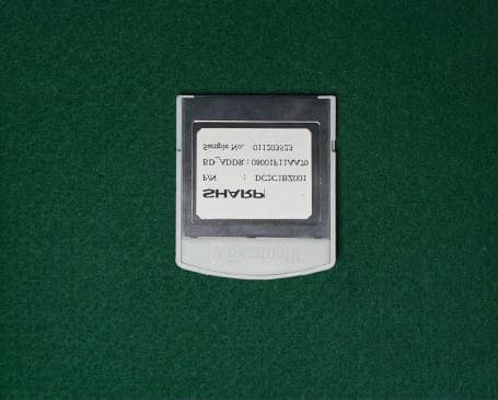
Click to zoom
Application Details
- Equipment Class
- DSS - Part 15 Spread Spectrum Transmitter
- Date of Grant
- Feb 19, 2002
- Application Purpose
- Original Equipment
- Date of Application
- Feb 19, 2002
- Equipment Note
- Bluetooth Transceiver Module
- Frequency Range
- 2402.00000000 - 2480.00000000
- Company
- Sharp Corporation
- Country
- Japan
Documents & Files
Document Text
Text extracted from the exhibit documents filed with the FCC. Open a document above to read the original.
Users Manual
1 DOC NO.EU-01Z05A Bluetooth CF Card DC2C1BZ001 User’s Manual DC2C1BZ001 User’s Manual DOC NO.EU-01Z05A 2 << DESCRIPTION >> This user’s manual covers the Sharp Bluetooth TM CF Card model DC2C1BZ001 intended for design application use with PDAs, Notebook PCs, mobile phones, digital cameras or PC peripherals. (Source: Bluetooth V.1.1 Radio specification Part A) Ref no. of QPN : 010-7LI_1 *QPN : Qualification Product Notice This device complies with Part 15 of the FCC Rules. Operation is subject to the following two conditions: (1) this device may not cause harmful interference, and (2) this device must accept any interference received, including interference that may cause undesired operation. << REMARK >> (1) This CF card is not designed for use in Life Support Application products where malfunction of those products can be reasonably expected to result in personal injury. SHARP customers using or selling these products for use in such applications do so at their risk and agree to fully indemnify SHARP for any damages resulting from such improper use or sale. (2) Country of origin: Japan or China. << NOTICE >> This equipment has been tested and found to comply with the limits for a Class B digital device, pursuant to part 15 of the FCC Rules. These limits are designed to provide reasonable protection against harmful interference in a residential installation. This equipment generates, uses and can radiate radio frequency energy and, if not installed and used in accordance with the instructions, may cause harmful interference to radio communications. However, there is no guarantee that interference will not occur in a particular installation. If this equipment does cause harmful interference to radio or television reception, which can be determined by turning the equipment off and on, the user is encouraged to try to correct the interference by one or more of the following measures: -Reorient or relocate the receiving antenna -Increase the separation between the equipment and receiver. -Connect the equipment into an outlet on a circuit different from that to which the receiver is connected. -Consult the dealer or an experienced radio/TV technician for help. This transmitter complies with FCC radiation exposure limits set forth for an uncontrolled environment. To comply with the FCC RF exposure compliance requirements, no change to the antenna or the device is permitted. Any change to the antenna or the device could result in the device exceeding the RF exposure requirements and void user. In addition, this transmitter must not be co-located or operating in conjunction with any other antenna or transmitter. << FCC WARNING >> Changes or modifications not expressly approved by the party responsible for compliance could void the user’s authority to operate the equipment. DC2C1BZ001 User’s Manual DOC NO.EU-01Z05A 3 1. INSTALL a) Insert CF card to CF card slot or PC card slot with CF card Adapter card. b) PC detect CF card and pop up the window. Push Next button. c) Select “Display a list of all .....” and push Next button. DC2C1BZ001 User’s Manual DOC NO.EU-01Z05A 4 d) Select “Ports[COM & LPT]” and push Next button. e) Select “Communication Point” and push Next button. f) Pop up the warning window, push Yes button. DC2C1BZ001 User’s Manual DOC NO.EU-01Z05A 5 g) Push Next button. h) Push Finish button. DC2C1BZ001 User’s Manual DOC NO.EU-01Z05A 6 2. HOW TO USE BLUETOOTH This Bluetooth Card has under HCI protocol. You can use the HCI command through the COM port There is Bluetooth specification on http://www.bluetooth.com/ 3. GENERAL SPECIFICATIONS 1-1 Bluetooth Specification Power Class 3 1-2 Frequency range 2402 MHz to 2480 MHz 1-3 Channel system TDMA 1-4 Duplex system Half duplex/TDD 1-5 Total number of channels 79 ch 1-6 Nominal antenna impedance 50 ohm 1-7 Intermediate frequency Zero IF 1-8 Modulation system GFSK/ BbT= 0.5 (Air Interface) Data rate: 1Mbps Process gain Frequency hopping 1600hops/sec 1-9 Operating voltage Vcc: 3.3 V+/-5% 1-10 Absolute maximum supply voltage Vcc: 4.0 V (Ta=25 deg.) 1-11 Weight 13 g/ typ. DC2C1BZ001 User’s Manual DOC NO.EU-01Z05A 7 4. DIMENSION AND MOUNTING DETAILS DRAFT
External Photos
<External Photos> Right view FCC ID:APYSJY0007 Left view FCC ID:APYSJY0007 Bottom view FCC ID:APYSJY0007 Top view FCC ID:APYSJY0007 Front view FCC ID:APYSJY0007 Rear view FCC ID:APYSJY0007
ID Label/Location Info
FCC ID:APYSJY0007
Internal Photos
<Internal Photos> Circuit board <front view> FCC ID:APYSJY0007 Circuit board <rear view> FCC ID:APYSJY0007
Operational Description
DOC NO. EU-01Z03 Bluetooth CF Card DC2C1BZ001 Technical Documentation MODEL: DC2C1BZ001 PAGE 1 DOC NO.EU-01Z03 SHARP CONFIDENTIAL AND PROPRIETARY This material embodies our copyright and know-how. You may not copy or disclose any parts of the material to any third party without our authorization. ELECTRONIC COMPONENTS (ELECOM) GROUP SHARP CORPORATION Description: This specification covers the Sharp Bluetooth TM CF Card model DC2C1BZ001 intended for design application use with PDAs, Notebook PCs, mobile phones, digital cameras or PC peripherals. (Source: Bluetooth V.1.1 Radio specification Part A) Ref no. of QPN : 010-7LI_1 *QPN : Qualification Product Notice Remark: 1.This CF card is not designed for use in Life Support Application products where malfunction of those products can be reasonably expected to result in personal injury. SHARP customers using or selling these products for use in such applications do so at their risk and agree to fully indemnify SHARP for any damages resulting from such improper use or sale. 2.Country of origin: Japan or China. [1] GENERAL SPECIFICATIONS 1-1 Bluetooth Specification Power Class 3 1-2 Frequency range 2402 MHz to 2480 MHz 1-3 Channel system TDMA 1-4 Duplex system Half duplex/TDD 1-5 Total number of channels 79 ch 1-6 Nominal antenna impedance 50 ohm 1-7 Intermediate frequency Zero IF 1-8 Modulation system GFSK/ BbT= 0.5 (Air Interface) Data rate: 1Mbps Process gain Frequency hopping 1600hops/sec 1-9 Operating voltage Vcc: 3.3 V+/-5% 1-10 Absolute maximum supply voltage Vcc: 4.0 V (Ta=25 deg.) 1-11 Weight 13 g/ typ. 1-12 Block diagram Figure 1 [2] MECHANICAL SPECIFICATIONS 2-1 Dimension and mounting details Figure 2 2-2 Terminal details Table 2 [3] ENVIRONMENT SPECIFICATIONS 3-1 Operating temperature 15 to 35 deg. ....Normal condition/ Radio spec Part A 0 to 35 deg. ......Extreme condition/ Radio spec Part A 0 to 50 deg. ......Application guaranteed condition 3-2 Storage temperature -20 to 70 deg.. 3-3 Efficient humidity Less than 85 % 3-4 Storage humidity Less than 90 % [4] TESTING CONDITIONS 4-1 Supply voltage Vcc: 3.3+/-0.1 V 4-2 Ambient temperature 25 +/- 3 deg.. 4-3 Ambient humidity 65 +/- 10 % Bluetooth is trademark owned by Telefonaktiebolaget L M Ericsson, Sweden and licensed to promoters and adopters of Bluetooth Special interest Group. CompactFlash and CF+ are trademarks of the CompactFlash Association. MODEL: DC2C1BZ001 PAGE 2 DOC NO.EU-01Z03 SHARP CONFIDENTIAL AND PROPRIETARY This material embodies our copyright and know-how. You may not copy or disclose any parts of the material to any third party without our authorization. ELECTRONIC COMPONENTS (ELECOM) GROUP SHARP CORPORATION [5] ELECTRICAL SPECIFICATIONS *** The following items should be measured under the “[4] TESTING CONDITIONS” if there are no comments in the condition table. *** Extreme condition: 0 to 35 degree. Normal condition: 15 to 35 degree. NO. Item Specification Condition Min Typ Max Unit << TX BLOCK >> 5-1 Output power/ Average -6.0 0.0 dBm Extreme condition, DH5, PRBS9 mod. 5-2 Power density 20 dBm Extreme condition, DH5, PRBS9 mod. 5-3 Frequency Range 2400 2483.5 MHz Extreme condition, DH1, PRBS9 mod. 5-4 20dB Bandwidth 1.0 MHz Extreme condition, DH1, PRBS9 mod. Adjacent channel power M +/- 2 ch -20 5-5 M > +/- 3 ch -40 dBm Extreme condition, DH1, PRBS9 mod. +/-140 +/-175 kHz Extreme condition, DH1, 11110000 mod. 5-6 Modulation characteristics +/-115 kHz Extreme condition, DH1, 1010 mod. 5-7 Initial carrier frequency tolerance +/-75 kHz Extreme condition, DH1, PRBS9 mod. 5-8 Carrier frequency drift kHz 1 slot packet/ DH1 +/- 25 3 slot packet/ DH3 +/-40 5 slot packet/ DH5 +/-40 Extreme condition, DH1, 1010 mod. Out-of band Spurious emissions / Conductive mode 30 to 1000MHz -36 1 to 12.75GHz -30 1.8 to 1.9GHz -47 5-9 5.15 to 5.3GHz -47 dBm Extreme condition, DH1, PRBS9 mod. << RX BLOCK >> 5-10 Receiver sensitivity DH1 & DH5 -70 dBm Extreme condition at B.E.R=1e-3, PRBS9 mod. C/I performance (X dB=D-UD *1) *2 Y=M(Co-channel) +14 Y=M +/-1 +4 Y=M +/-2 -30 dB Normal condition D level : -60 dBm, DH1, PRBS9 mod. UD level : at B.E.R=1e-3, PRBS9 mod. 5-11 Y=M> +/-3 -40 dB Normal condition D level : -67 dBm, DH1, PRBS9 mod. UD level : at B.E.R=1e-3, PRBS9 mod. *1 UD...Undesired signal level(dBm) D...Desired signal level(dBm) Y : undesired-channel M : desired-channel M +/- 1 : adjacent channel M +/- 2 : next adjacent channel *2 Frequencies where the requirements are not met are called spurious response frequencies. Five spurious response frequencies are allowed at frequencies with a distance of .2 MHz from the wanted signal. On these spurious response frequencies a relaxed interference requirement C/I = -17 dB shall be met. MODEL: DC2C1BZ001 PAGE 3 DOC NO.EU-01Z03 SHARP CONFIDENTIAL AND PROPRIETARY This material embodies our copyright and know-how. You may not copy or disclose any parts of the material to any third party without our authorization. ELECTRONIC COMPONENTS (ELECOM) GROUP SHARP CORPORATION Blocking performance 30 to 1910 MHz -10 1910 to 2000 MHz -10 2000 to 2399 MHz -27 2500 to 3000 MHz -27 5-12 *3 3 to 12.75 GHz -10 dBm Normal condition D : 2460MHz only, -67 dBm , DH1, PRBS9 mod. UD level : at B.E.R=1e-3, No-mod. 5-13 Intermodulation performance -39 dBm Normal condition D level : -64 dBm, DH1, PRBS9 mod. UD level : at B.E.R=1e-3, PRBS9 mod. UD1:Y=M +/- 3, No-mod. UD2:Y=M +/- 6, PRBS9 mod. 5-14 Maximum input level -20 dBm Normal condition at B.E.R=1e-3, PRBS9 mod. Spurious emission when not allocated a TX ( TX circuit : turned off ) 30 to 1000 MHz -57 5-15 1 to 12.75GHz -47 dBm Normal condition, DH1, PRBS9 mod. << TOTAL BLOCK >> Current consumption (TX mode) Peak current: TX (continuous) 100 5-16 Peak current: RX(continuous) 100 mA * current consumption under burst mode is depends on software. *3 24 exceptions are permitted which are dependent upon the given receive channel frequency and are centered at a frequency which is an integer multiple of 1MHz. At 19 of these …
Text truncated - open the document above for the full version.
Test Report
A-PEX INTERNATIONAL CO., LTD. YOKOWA NO.3 OPEN SITE COMPANY : SHARP CORPORATIONREPORT NO : 22CE0007-YW EQUIPMENT : Bluetooth CF CardREGULATION : Fcc Part15SubpartC 247/209 MODEL : DC2C1BZ0001TEST DISTANCE : 3m(1 to 10GHz)/1m(10 to 26GHz) FCC ID : APYSJY0007DATE : 2002 / 1 / 25 POWER : AC120V/60HzTemp. / Humi. : 22deg.C / 39% Mode : Transmitting(ch02:2402MHz) ENGINEER : Naoki Sakamoto PK DETECT(S/A : RBW 1MHz and VBW 1MHz) No.FREQS/A READINGANTAMPCABLEH.P.FilterRESULTLimitMARGIN HORVERFactorGAINLOSSHORVERPKHORVER [GHz][dBuV][dBuV][dB][dB][dB][dB][dBuV/m][dBuV/m][dBuV/m][dB][dB] #11.3001956.259.926.335.02.60.050.153.874.024.724.2 #21.9026852.153.729.734.53.30.050.652.274.023.421.8 #32.3900046.845.531.338.13.60.043.642.374.030.431.7 44.8040041.941.735.434.58.01.151.951.774.022.122.3 57.2060642.144.439.134.89.40.556.358.674.017.715.4 69.6079943.043.439.235.011.00.558.759.174.015.314.9 *712.0100042.843.343.534.412.10.564.565.083.519.018.5 *814.4120043.142.942.233.113.50.666.366.183.517.217.4 *916.8140043.844.043.833.414.80.669.669.883.513.913.7 *1019.2160043.943.938.033.415.81.065.365.383.518.218.2 *1121.6180044.043.637.833.016.50.665.965.583.517.618.0 *1224.0200044.644.139.633.215.80.767.567.083.516.016.5 AV DETECT(S/A : RBW 1MHz and VBW 10Hz) No.FREQS/A READINGANTAMPCABLEH.P.FilterRESULTLimitMARGIN HORVERFactorGAINLOSSHORVERAVHORVER [GHz][dBuV][dBuV][dB][dB][dB][dB][dBuV/m][dBuV/m][dBuV/m][dB][dB] #11.3001940.042.726.335.02.60.033.936.654.020.117.4 #21.9026837.553.629.734.53.30.036.052.154.018.01.9 #32.3900035.334.431.338.13.60.032.131.254.021.922.8 44.8040031.831.035.434.58.01.141.841.054.012.213.0 57.2060633.034.339.134.89.40.547.248.554.06.85.5 69.6079932.533.239.235.011.00.548.248.954.05.85.1 *712.0100032.132.343.534.412.10.553.854.063.59.79.5 *814.4120031.932.142.233.113.50.655.155.363.58.48.2 *916.8140032.832.943.833.414.80.658.658.763.54.94.8 *1019.2160032.532.638.033.415.81.053.954.063.59.69.5 *1121.6180032.932.937.833.016.50.654.854.963.58.78.7 *1224.0200033.633.339.633.215.80.756.556.263.57.17.4 Sample Calculation : RESULT=Reading + ANT Factor - Amp Gain + CABLE LOSS + High Pass Filter Except for the above table : All other spurious emissions are more than 20dB below the limit. * Test Distance 1m, 1m Limit=3m Limit(54dB)+20log(3/1) # The point don't use high pass filter. P. A4 DATA OF SUPURIOUS EMISSIONS(1GHz to 26GHz) A-PEX INTERNATIONAL CO., LTD. YOKOWA NO.3 OPEN SITE COMPANY : SHARP CORPORATIONREPORT NO : 22CE0007-YW EQUIPMENT : Bluetooth CF CardREGULATION : Fcc Part15SubpartC 247/209 MODEL : DC2C1BZ0001TEST DISTANCE : 3m(1 to 10GHz)/1m(10 to 26GHz) FCC ID : APYSJY0007DATE : 2002 / 1 / 25 POWER : AC120V/60HzTemp. / Humi. : 22deg.C / 39% Mode : Transmitting(ch80:2480MHz) ENGINEER : Naoki Sakamoto PK DETECT(S/A : RBW 1MHz and VBW 1MHz) No.FREQS/A READINGANTAMPCABLE H.P.FilterRESULTLimitMARGIN HORVERFactorGAINLOSSHORVERPKHORVER [GHz][dBuV][dBuV][dB][dB][dB][dB] [dBuV/m][dBuV/m][dBuV/m][dB][dB] #11.2973656.158.126.335.02.60.050.052.074.024.022.0 #21.8963651.453.129.734.53.30.049.951.674.024.122.4 #32.4835054.355.431.638.13.70.051.552.674.022.521.4 44.9600040.440.735.834.57.91.150.751.074.023.323.0 57.4400041.540.939.234.99.50.555.855.274.018.218.8 69.9200041.541.339.234.911.00.557.357.174.016.716.9 *712.3999943.342.843.334.212.30.565.264.783.518.318.8 *814.8799944.243.042.933.013.70.568.367.183.515.216.4 *917.3599943.544.143.933.114.80.669.770.383.513.813.2 *1019.8400043.843.738.033.416.01.666.065.983.517.517.6 *1122.3200043.143.438.333.016.50.365.265.583.518.418.1 *1224.8000043.644.239.433.215.41.066.266.883.517.316.7 AV DETECT(S/A : RBW 1MHz and VBW 10Hz) No.FREQS/A READINGANTAMPCABLE H.P.FilterRESULTLimitMARGIN HORVERFactorGAINLOSSHORVERAVHORVER [GHz][dBuV][dBuV][dB][dB][dB][dB] [dBuV/m][dBuV/m][dBuV/m][dB][dB] #11.2973641.442.626.335.02.60.035.336.554.018.717.5 #21.8963639.239.729.734.53.30.037.738.254.016.315.8 #32.4835053.854.931.638.13.70.051.052.154.03.01.9 44.9600031.131.335.834.57.91.141.441.654.012.612.4 57.4400031.430.739.234.99.50.545.745.054.08.39.0 69.9200029.830.539.234.911.00.545.646.354.08.47.7 *712.3999931.831.743.334.212.30.553.753.663.59.89.9 *814.8799932.032.242.933.013.70.556.156.363.57.47.2 *917.3599932.632.943.933.114.80.658.859.163.54.74.4 *1019.8400032.632.938.033.416.01.654.855.163.58.78.5 *1122.3200032.532.838.333.016.50.354.654.963.59.08.7 *1224.8000033.733.839.433.215.41.056.356.463.57.27.1 Sample Calculation : RESULT=Reading + ANT Factor - Amp Gain + CABLE LOSS Except for the above table : All other spurious emissions are more than 20dB below the limit. * Test Distance 1m, 1m Limit=3m Limit(54dB)+20log(3/1) # The point don't use high pass filter. P. A5 DATA OF SUPURIOUS EMISSIONS(1GHz to 26GHz) A-PEX INTERNATIONAL CO., LTD. YOKOWA NO.3 OPEN SITE COMPANY : SHARP CORPORATIONREPORT NO : 22CE0007-YW EQUIPMENT : Bluetooth CF CardREGULATION : Fcc Part15SubpartC 247/209 MODEL : DC2C1BZ0001TEST DISTANCE : 3m FCC ID : APYSJY0007DATE : 2002 / 1 / 25 POWER : AC120V/60HzTemp. / Humi. : 22deg.C / 39% Mode : Receiving ENGINEER : Naoki Sakamoto PK DETECT(S/A : RBW 1MHz and VBW 1MHz) No.FREQS/A READINGANTAMPCABLERESULTLimitMARGIN HORVERFactorGAINLOSSHORVERPKHORVER [GHz][dBuV][dBuV][dB][dB][dB] [dBuV/m][dBuV/m][dBuV/m][dB][dB] 11.2973655.558.926.335.02.649.452.874.024.621.2 21.8963652.253.529.734.53.350.752.074.023.322.0 AV DETECT(S/A : RBW 1MHz and VBW 10Hz) No.FREQS/A READINGANTAMPCABLERESULTLimitMARGIN HORVERFactorGAINLOSSHORVERAVHORVER [GHz][dBuV][dBuV][dB][dB][dB] [dBuV/m][dBuV/m][dBuV/m][dB][dB] 11.2973641.043.126.335.02.634.937.054.019.117.0 21.8963639.239.629.734.53.337.738.154.016.315.9 Sample Calculation : RESULT=Reading + ANT Factor - Amp Gain + CABLE LOSS. Except for the above table : All other spurious emissions are more than 20dB below the limit. P. A6 DATA OF SUPURIOUS EMISSIONS(1GHz to 26GHz) Report No : 22CE0007-YW A 7 Report No : 22CE0007-YW A 8 Report No : 22CE0007-YW A 9 Report No : 22CE0007-YW A 10
Test Report
Test report FCC ID : APYSJY0007 Our reference : 22CE0007-YW-2 Page: 2 of 16 Issued date: January 18, 2002 A-pex International Co., Ltd. YOKOWA LAB. 108 Yokowa-cho, Ise-shi, Mie-ken 516-1106 JAPAN Telephone:int +81 596 39 1485 Facsimile: int +81 596 39 0232 Table of Contents Page 1 GENERAL INFORMATION3 1.1 Tested Methodology4 1.2 Test Facility4 2 PRODUCT DESCRIPTION5 2.1Test system Details5 3 SYSTEM TEST CONFIGURATION7 3.1 Justification7 3.2.Configuration of Tested System7 4 MEASUREMENT UNCERTAINTY9 5 TEST INSTRUMENTS10 6 SUMMARY OF TEST11 6.1 §15.207 Conducted Emissions11 6.2 §15.247(a)(1) Frequency Hopping Systems11 6.3 §15.247(a)(1)(ii) Channel Utilization11 6.4 §15.247(b) Maximum Peak Out Put Power(Radiated)12 6.5 §15.247(b) Maximum Peak Out Put Power(Conducted)12 6.6 §15.247(c) Out of Band Emissions(Radiated)13 6.7 §15.247(c) Out of Band Emissions(Conducted)13 Photographs of test setup 14-15 APPENDIX16 Test dataA1toA26 Test report FCC ID : APYSJY0007 Our reference : 22CE0007-YW-2 Page: 3 of 16 Issued date: January 18, 2002 A-pex International Co., Ltd. YOKOWA LAB. 108 Yokowa-cho, Ise-shi, Mie-ken 516-1106 JAPAN Telephone:int +81 596 39 1485 Facsimile: int +81 596 39 0232 1 GENERAL INFORMATION APPLICANT: SHARP CORPORATION ADDRESS: 22-22, Nagaike-cho, Abeno-ku, Osaka, 545-8522 Japan TEL: 81-6-6624-3857 FAX: 81-6-6622-9289 REGULATION(S): FCC Part15 Subpart C, Section 15.247 MODEL NUMBER: DC2C1BZ001 SERIAL NUMBER: 011203521 KIND OF EQUIPMENT: Bluetooth CF Card TESTED DATE: December 5 and 6, 2001 RECEIPT DATE OF SAMPLE : December 5, 2001 REPORT FILE NUMBER: 22CE0007-YW-2 TEST SITE: A-PEX Yokowa No.3 Open Test Sites Test report FCC ID : APYSJY0007 Our reference : 22CE0007-YW-2 Page: 4 of 16 Issued date: January 18, 2002 A-pex International Co., Ltd. YOKOWA LAB. 108 Yokowa-cho, Ise-shi, Mie-ken 516-1106 JAPAN Telephone:int +81 596 39 1485 Facsimile: int +81 596 39 0232 1.1 Tested Methodology The measurement was performed according to the procedures in ANSI C63.4(1992). 1.2 Test Facility The open area site measurement facilities used to collect the radiated data are located at 108, Yokowa-cho, Ise-shi, Mie-ken, 516-1106 Japan. These sites have been fully described in reports submitted to the FCC office. No.1 and No.3 test site has filed to the FCC on September 12, 2000 as number: 90412 and is accepted by Industry Canada on May 01, 2001 as number IC2973-3. Test report FCC ID : APYSJY0007 Our reference : 22CE0007-YW-2 Page: 5 of 16 Issued date: January 18, 2002 A-pex International Co., Ltd. YOKOWA LAB. 108 Yokowa-cho, Ise-shi, Mie-ken 516-1106 JAPAN Telephone:int +81 596 39 1485 Facsimile: int +81 596 39 0232 2 PRODUCT DESCRIPTION SHARP CORPORATION, Model DC2C1BZ001 (referred to as the EUT in this report) is a Bluetooth CF Card. The EUT is based on the Bluetooth SPEC. V1.1 and CF Card Rev. 1.4. The specification is as following : Frequency characteristies: 2402MHz through 2480MHz No. of channels / channel spacing : 79 channels / 1MHz channel spacing Modulation: GFSK (Low power Frequency Hopping Spread Spectrum(FHSS)) Antenna type: Integral Antenna Gain: -2.4dBi Operating Voltage: DC3.3V *FccPart15.203 Antenna requirement Since the antenna of Bluetooth CF card is incorporated in a equipment and it is impossible to be modified by user, therefore this requirement is satisfied. Also however there is a antenna connector for maintenance at external of equipment, specific connector is used as showed in attachment "A26" then it can not be used by general user. Test report FCC ID : APYSJY0007 Our reference : 22CE0007-YW-2 Page: 6 of 16 Issued date: January 18, 2002 A-pex International Co., Ltd. YOKOWA LAB. 108 Yokowa-cho, Ise-shi, Mie-ken 516-1106 JAPAN Telephone:int +81 596 39 1485 Facsimile: int +81 596 39 0232 2.1 Test System Details Description of EUT and support equipment No.ItemModel numberSerial numberManufacturerRemark (FCC ID) ABluetooth CF CardDC2C1BZ001011203521SHARPAPYSJY007 (EUT) BNotebook PCPC-PJ100S09047864SHARPA00-0198JP CAC AdaptorEA-J03VLTD0015016173SHARP- D*Floppy Disk DriveCE-FD04-SHARP- E*Microphone--FUJITSU- F*MouseM-UB 48830318-0000SHARPDZL211137 G*Speaker000M3A2-0--- H*CRT MonitorD5258ATH02905902Hewlett Packard- I*ModemC202A010303EPSONBKM552C202A J*AC AdaptorH00CAA017321EPSON- * Only Conducted Emission :AC Line List of cables used No.NameLength (m)ShieldBackshell materialRemark 1DC Power Cable1.2NPolyvinyl chloride- 2AC Power Cable1.8NPolyvinyl chloride- 3*Floppy Disk Drive Cable0.3YPolyvinyl chloride- 4*Microphone Cable1.6NPolyvinyl chloride- 5*Mouse Cable0.7YPolyvinyl chloride- 6*Speaker Cable1.6NPolyvinyl chloride- 7*RGB Cable1.3YPolyvinyl chloride- 8*AC Power Cable1.8NPolyvinyl chloride- 9*RS232C Cable1.5YPolyvinyl chloride- 10*AC Power Cable1.8NPolyvinyl chloride- * Only Conducted Emission :AC Line Test report FCC ID : APYSJY0007 Our reference : 22CE0007-YW-2 Page: 7 of 16 Issued date: January 18, 2002 A-pex International Co., Ltd. YOKOWA LAB. 108 Yokowa-cho, Ise-shi, Mie-ken 516-1106 JAPAN Telephone:int +81 596 39 1485 Facsimile: int +81 596 39 0232 3 SYSTEM TEST CONFIGURATION 3.1 Justification The system was configured in typical fashion (as a customer would normally use it) for testing. Test mode : Transmitting mode Performed the test about channels 2(low:2402MHz), 41(mid:2441MHz) and 80(high:2480MHz) among 79 channels of all Carrier frequencies. Receiving mode 3.2 Configuration of Tested System Figure 3.2.1 Configuration of Tested System AC 120V/60Hz 1 Wooden table 2 A C B : Ferrite Core Test report FCC ID : APYSJY0007 Our reference : 22CE0007-YW-2 Page: 8 of 16 Issued date: January 18, 2002 A-pex International Co., Ltd. YOKOWA LAB. 108 Yokowa-cho, Ise-shi, Mie-ken 516-1106 JAPAN Telephone:int +81 596 39 1485 Facsimile: int +81 596 39 0232 Figure 3.2.2 Configuration of Tested System (Only Conducted emission: AC Lines) AC 120V/60Hz : Ferrite Core A AC 120V/60Hz D J I H E C F B 4 9 6 7 8 1 10 5 2 3 G G Test report FCC ID : APYSJY0007 Our reference : 22CE0007-YW-2 Page: 9 …
Text truncated - open the document above for the full version.
Test Report
Processing Gain Document for FCC ID:APYSJY0007 1. Introduction This document describes requirements and measurement results for the processing gain in accordance with the Sub-clause 15.247 of FCC Part 15. This report includes the test method and procedure. 2. FCC Requirement FCC requires for FHSS systems operating in the 2.4 GHz band to use at least 75 hopping channels in the FCC 15.247. In normal communication the channel hopping system is represented by a pseudo- random hopping sequence through the 79 channels. Therefore, the system meets the FCC requirement. During the inquiry or paging mode, however, the system only uses 32 hopping channels. In these modes the system is regarded as a combination of both direct sequence and frequency hopping modulation techniques, and the system is required to achieve a processing gain of at least 17 dB from the combined techniques in the Sub-clause 15.247(f) of FCC Part 15. Since the use of 32 hopping channels during the inquiry or paging mode is equivalent to 15.1 dB of processing gain, further processing gain must be achieved by the direct sequence operation of the access code. As a result at least 1.9 dB processing gain must be demonstrated by the measurement. 3. FCC Proposal of the Processing Gain Measurement FCC proposes the jamming margin test method to demonstrate the processing gain of the DSSS component in APPENDIX C of the FCC Public Notice 97-114 and also in the Sub- clause 15.247(e)(2) of FCC Part 15. In the APPENDIX the proposal describes measurement method in detail with a configuration of jamming test setup; The Processing Gain may be measured using the CW jamming margin method. The test consists of stepping a signal generator in 50 kHz increments across the pass-band of the system. At each point, the generator level required to produce the recommended Bit Error Rate (BER) is recorded. This level is the jammer level. The output power of the transmitting unit is measured at the same point. The Jammer to Signal (J/S) ratio is then calculated. Discarded the worst 20 percents of the J/S data points. The lowest remaining J/S ratio is used when calculating the Processing Gain. In a practical system, there are always implementation losses which degrade the performance below that of an optimal theoretical system of the same type. Losses occur due to non-optimal filtering, lack of equalization, LO phase noise, “corner cutting in digital processing”, etc. Total losses in a system, including transmitter and receiver, should be assumed to be no more than 2 dB. In order to calculate the Processing Gain (Gp) of the system, the following equation is used: Gp =(S/N)o + Mj + Lsys where, (S/N)o = Signal to noise ratio Mj = J/S ratio Lsys = System losses. 4. Test Arrangement and Test Procedure Figure 1 shows the measurement block diagram with the list of equipment used. The generator, AMIQ, generates I/Q modulation data and is installed a BER measurement function as the option. SMIQ is an RF signal generator for desired signal. The signal generator, SMP, generates Jammer signals for undesired signal. The dual directional coupler, Agilent 778, combines the desired and undesired signals and outputs the combined signal to the DUT (device under test). Demodulated signals from the DUT are sent to AMIQ through a level converter and are compared with original signals to measure bit errors. Two PC’s are used for DUT control and BER calculation, respectively. The following test procedure is used to verify the processing gain of DS component for the receiver: 1. Hopping off. Bluetooth transmitter (SMIQ) at an arbitrary fc (for example, 2441 MHz) chosen from the inquiry/paging hopping sequence. 2. CW jammer starts at fc. 3. Bluetooth transmitter (SMIQ) sends access codes (for example, 65B333) at signal level S. The timing of the transmitter signal is aligned to the scan window of the DUT (device under test) receiver. 4. Based on the correlation output of the DUT receiver, bit errors are counted. 5. Jammer level J is increased until BER requirement is violated (> 1x10e-3). The BER will be calculated based on 1x10e4 transmitted access codes. 6. This J/S level is recorded. 7. Jammer signal frequency 50 kHz is increased/decreased. 8. Steps 3 to 7 is repeated until the J/S values are comfortably compliant. 9. The processing gain is calculated as described in the FCC procedure: Discarding the worst 20 percents of the J/S data points, the lowest remaining J/S ratio is used to calculate the processing gain, as follows: Gp = (S/N)o + (J/S) + Lsys 5. Measurement Results Test conditions are: (a) Signal to noise ratio (S/N)o (S/N)o is required signal to noise ratio at the receiver input for a BER 1x10e-3. The ideal equation/curve for GFSK is used to determine this value. For the DUT a signal to noise ratio of 16.4 dB is given. The system loss Lsys of maximal 2 dB is included. (b) Jammer to signal ratio (J/S) (J/S) is measured according to the test setup. The test result are shown with the processing gain calculation in Fig. 2. After discarding the worst 20 percents of the J/S data points, the lowest J/S data is found at -400 kHz and +400 kHz. The measured processing gain during inquiry and paging modes shows 2.8 dB. As a result the total processing gain is 17.9 dB (15.1 dB + 2.8 dB). 6. Conclusion During normal communication, all 79 hopping channels are always used and the DUT complies with FCC requirement in the sub-clause 15.247(b)(1) of the FCC Part 15. During inquiry and paging modes, the DUT is regarded as a hybrid system employing a combination of both direct sequence and frequency hopping modulation techniques and complies with FCC requirement in the sub-clause 15.247(f) of the FCC Part 15 from measurement results described in this report. Fig. 1 Measurement Arrangement and Equipment List EquipmentFunctionTypeManufacturer R&S AMIQI/Q Modulation DATA GeneratorAMIQRohde&Schwar z R&S SMIQRF Signal GeneratorSMIQ03BRohde&Schwar z R&S SGRF Signal GeneratorSMP02Rohde&Schwar z …
Text truncated - open the document above for the full version.
Test Setup Photos
Test report FCC ID : APYSJY0007 Our reference : 22CE0007-YW Page: 10 of 11 Issued date: January 28, 2002 A-pex International Co., Ltd. YOKOWA LAB. 108 Yokowa-cho, Ise-shi, Mie-ken 516-1106 JAPAN Telephone:int +81 596 39 1485 Facsimile: int +81 596 39 0232 Photographs of test setup(1)
Test Setup Photos
<Test setup photos> FCC ID:APYSJY0007 FCC ID:APYSJY0007 FCC ID:APYSJY0007
Contact Information
Applicant
Taihei Ohtsuka(Deputy Division Manager, ESG & Q promotion unit)
Technical Contact
A-Pex International Co., Ltd.Naoki Sakamoto
[email protected]+81 596 39 1485
108 Yokowa-cho · Ise-chi, Mie-ken · Japan
Test Firm
UL Japan, Inc.Kazunori Nishimura
Technical Specifications
| # | Rule Parts | Frequency Range | Power Output |
|---|---|---|---|
| 1 | 15C | 2.40 GHz - 2.48 GHz | 580.00 µW |
Other Applications from Sharp Corporation
APYHRO00343
Aug 17, 2026Smartphone
Equipment Class
DTS - Digital Transmission SystemAPYHRO00342
Jul 29, 2026Smart phone
Equipment Class
DXX - Part 15 Low Power Communication Device TransmitterAPYHRO00341
May 28, 2026Smart phone
Equipment Class
DTS - Digital Transmission SystemAPYHRO00340
Dec 01, 2025BT remote control
Equipment Class
DTS - Digital Transmission SystemAPYHRO00339
Sep 17, 2025Smart phone
Equipment Class
NII - Unlicensed National Information Infrastructure TX