AZY-HF-LPB200WiFi Module
High-Flying Electronics Technology Co.,Ltd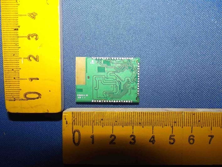
Click to zoom
Application Details
- Equipment Class
- DTS - Digital Transmission System
- Date of Grant
- Dec 03, 2013
- Application Purpose
- Original Equipment
- Date of Application
- Dec 03, 2013
- Equipment Note
- WiFi Module
- Frequency Range
- 2422.00000000 - 2452.00000000
- Country
- China
Documents & Files
Document Text
Text extracted from the exhibit documents filed with the FCC. Open a document above to read the original.
Users Manual
HF-LPB200 Low Power WiFi Module User Manual Shanghai High-Flying Electronics Technology Co., Ltd www.hi-flying.com - 1 - HF-LPB200 Low Power WiFi Module User Maunal V 1.0 Overview of Characteristic Support IEEE802.11b/g/n Wireless Standards Marvell Solutions for Smart Energy and Home/Building Automation Low-Power Applications with Excellent Power Save Scheme Support UART/SPI/USB/PWM/ADC/GPIO Data Communication Interface Support Work As STA/AP/AP+STA/Wi-Fi Direct Mode Support Smart Link TM Function (APP for smart configuration) Support Wireless (OTA) and Remote Firmware Upgrade Function Support Wakeup-on-Wireless and Wakeup Local Support FTTPS/TLS and mDNS Application Single +3.3V Power Supply Smallest Size: 23.1mm x 32.8mm x2.7mm FCC/CE Certificated HF-LPB200 Low Power WiFi Module User Manual Shanghai High-Flying Electronics Technology Co., Ltd www.hi-flying.com - 2 - TABLE OF CONTENTS LIST OF FIGURES ................................................................................................................................... 5 LIST OF TABLES ..................................................................................................................................... 6 HISTORY .................................................................................................................................................. 6 1. PRODUCT OVERVIEW................................................................................................................. 7 1.1. General Description ................................................................................................................. 7 1.1.1 Device Features .................................................................................................................. 7 1.1.2 Device Paremeters ............................................................................................................. 8 1.1.3 Key Application ................................................................................................................... 8 1.2. Hardware Introduction ............................................................................................................. 9 1.2.1. Pins Definition ..................................................................................................................... 9 2.1.1. Electrical Characteristics ................................................................................................... 11 2.1.2. Mechanical Size ................................................................................................................ 11 2.1.3. On-board Chip Antenna .................................................................................................... 12 2.1.4. External Antenna ................................................................................... 错误!未定义书签。 2.1.5. Evaluation Kit .................................................................................................................... 13 2.1.6. Order Information .............................................................................................................. 15 2.2. Typical Application ................................................................................................................ 16 2.2.1. Hardware Typical Application ............................................................................................ 16 2.2.2. Internal MCU Hardware Feature ....................................................................................... 17 2.2.3. Software SDK Architecture ............................................................................................... 18 3. FUNCTIONAL DESCRIPTION ................................................................................................... 19 3.1. Wireless Networking .............................................................................................................. 19 3.1.1. Basic Wireless Network Based On AP (Infrastructure) .................................................... 19 3.1.2. Wireless Network Based On AP+STA .............................................................................. 19 3.1.3. Wi-Fi Direct Network ......................................................................................................... 20 3.2. Work Mode : Transparent Transmission Mode ................................................................... 21 3.3. UART Frame Scheme ............................................................................................................. 22 3.4. Encryption............................................................................................................................... 22 3.5. Multi-TCP Link Connection ................................................................................................... 22 3.6. Power Save Scheme .............................................................................................................. 23 3.7. Parameters Configuration ..................................................................................................... 24 3.8. Firmware Update .................................................................................................................... 24 3.9. GPIO Function ........................................................................................................................ 25 3.10. Analog Digital Converter (ADC) Function ........................................................................ 26 4. OPERATION GUIDELINE........................................................................................................... 28 4.1. Configuration via Web Accessing ........................................................................................ 28 4.1.1. Open Web Management Interface ................................................................................... 28 4.1.2. System Page ..............................................…
Text truncated - open the document above for the full version.
Users Manual
FCC INFORMATION (additional) OEM INTEGRATION INSTRUCTIONS: This device is intended only for OEM integrators under the following conditions: The module must be installed in the host equipment such that 20 cm is maintained between the antenna and users, and the transmitter module may not be co-located with any other transmitter or antenna. The module shall be only used with the external antenna(s) that has been originally tested and certified with this module. As long as 3 conditions above are met, further transmitter test will not be required. However, the OEM integrator is still responsible for testing their end-product for any additional compliance requirements required with this module installed (for example, digital device emissions, PC peripheral requirements, etc.). Validity of using the module certification: In the event that these conditions cannot be met (for example certain laptop configurations or co-location with another transmitter), then the FCC authorization for this module in combination with the host equipment is no longer considered valid and the FCC ID of the module cannot be used on the final product. In these circumstances, the OEM integrator will be responsible for re-evaluating the end product (including the transmitter) and obtaining a separate FCC authorization. End product labeling: This transmitter module is authorized only for use in device where the antenna may be installed such that 20 cm may be maintained between the antenna and users. The final end product must be labeled in a visible area with the following: “Contains FCC ID: AZY-HF-LPB200”. Information that must be placed in the end user manual: The OEM integrator has to be aware not to provide information to the end user regarding how to install or remove this RF module in the user's manual of the end product which integrates this module. The end user manual shall include all required regulatory information/warning as show in this manual.
Cover Letter(s)
High-Flying Electronics Technology Co., Ltd FCC Confidentiality Request Number:CF303 Version:V05 Date: 21-05-2012 (Permanent or also called long term confidentiality is the normal method to keep certain docuements confidential, and may apply to schematics, block diagrams, operational description and bill of materials.) To: Federal Communications Commission Equipment Authorization Branch 7435 Oakland Mills Road Columbia, MD 21046 Pursuant to 47 CFR Section 0.459(a) & (b), we, (the applicant / grantee) Company nameHigh-Flying Electronics Technology Co., Ltd AddressRoom 511, #7Building, No.365 Chuanhong Road, Pudong, CityShanghai, CountryChina request for this certification filing under: Grantee CodeProduct Number FCC ID:AZY-HF-LPB200 to maintainpermanent confidentialityfor the following documents submitted within this application: (please cross what is applicable, or add other documents, provide the file name and description) ExhibitFile NameDescription √ Operational DescriptionOperational Descriptionexplaining the functioning of the block diagram √ Block DiagramsBlock Diagramsshowing the systematic building blocks of the EUT √ Schematics DiagramsSchematicsshowing components, their values and interconnection Bill of MaterialsList of components used on the PCB’s of the EUT Above materials crossed contain secrets, proprietary and technical information, which would customarily be guarded from competitors under 47 CFR, section 0.457(d)(2). Disclosure or publication or any portion of this company confidential material to other parties could cause substantial competitive harm and provide unjustified benefits for competitors. We understand that pursuant to 47 CFR section 0.457(d)(1)(ii) disclosure of the applicant and all accompanying documentation will not be made before the date of the grant. The documents indicated as confidential above, are not publicly available elsewhere. Attestation: City and Country:Date:Name: (this must be a person) Function:Signature: (or official company stamp) Shanghai, China2013-11-08 Sen XieGeneral Manager
Cover Letter(s)
High-Flying Electronics Technology Co., Ltd FCC Modular Approval Request Number:CF305 Version:V04 Date: 07-08-2012 To t he FCC or FCC TCB handling this application Hereby we, Company name (grantee)High-Flying Electronics Technology Co., Ltd AddresssRoom 511, #7Building, No.365 Chuanhong Road, Pudong, City / ZIP / State / CountryShanghai, China requestmodular approvalfor the certification of our equipment within this application, identified by: FCC ID:AZY-HF-LPB200 The table below contains the justification for modular approval of this equipment: Requirement per 15.212 and KDB 996369 D01 Module Certification Guide v01r03 Explanation from grantee(do not write yes / no, but explain why it complies / how it is achieved) 1. The modular transmitter must have its own RF shielding.The module has its own RF shielding. 2. The modular transmitter must have buffered modulation/data inputs (if such inputs are provided) to ensure that the module will comply with Part 15 requirements under conditions of excessive data rates or over-modulation. The modular has buffered data inputs, it is integrated in chip 88WE8782. 3. The modular transmitter must have its own power supply regulation. Yes, the modular transmitter(88WE8782) chipset has internal PMU (Power Management Unit) which generates power supplies required by the internal circuitry from the battery or support device. 4. The modular transmitter must comply with the antenna requirements of Section 15.203 and 15.204(c). The antenna must either be permanently attached or employ a “unique” antenna coupler (at all connections between the module and the antenna, including the cable).. The module meets the FCC antenna requirements, It has an unique connector. 5. The modular transmitter must be tested in a stand-alone configuration, i.e., the module must not be inside another device during testing. This is intended to demonstrate that the module is capable of complying with Part 15 emission limits regardless of the device into which it is eventually installed. The module was tested in a stand-alone configuration via a 10M/100M Ethernet network card. 6. The modular transmitter must be labeled with its own FCC ID number, and, if the FCC ID is not visible when the module is installed inside another device, then the outside of the device into which the module is installed must also display a label referring to the enclosed module. This exterior label can use wording such as the following: “Contains Transmitter Module FCC ID: XYZMODEL1” or “Contains FCC ID: XYZMODEL1.” Any similar wording that expresses the same meaning may be used. The Grantee may either provide such a label, an example of which must be included in the application for equipment authorization, or, must provide adequate instructions along with the module which explain this requirement. In the latter case, a copy of these instructions must be included in the application for equipment authorization. The label position o fFCC ID is clearly indicated. Please see the label location. 7. The modular transmitter must comply with any specific rule or operating requirements applicable to the transmitter and the manufacturer must provide adequate instructions along with the module to explain any such requirements. A copy of these instructions must be included in the application for equipment authorization. For example, there are very strict operational and timing requirements that must be met before a transmitter is authorized for operation under Section 15.231. For instance, data transmission is prohibited, except for operation under Section 15.231(e), in which case there are separate field strength level and timing requirements. Compliance with these requirements must be assured. The module is compliant with all applicable FCC rules. Datail instructions are given in the Users Manual. 8. The modular transmitter must comply with any applicable RF exposure requirements. For example, FCC Rules in Sections 2.1091, 2.1093 and specific Sections of Part 15, including 15.319(i), 15.407(f), 15.253(f) and 15.255(g), require that Unlicensed PCS, UNII and millimeter wave devices perform routine environmental evaluation for RF Exposure to demonstrate compliance. In addition, spread spectrum transmitters operating under Section 15.247 are required to address RF Exposure compliance in accordance with Section 15.247(b)(4). Modular transmitters approved under other Sections of Part 15, when necessary, may also need to address certain RF Exposure concerns, typically by providing specific installation and operating instructions for users, installers and other interested parties to ensure compliance. The module complies with the mobile and fixed 20cm separation distance location requirements. Attestation(by grantee) City and Country:Date:Name: (this must be a person) Function:Signature: (or official company stamp) Shanghai, China2013-11-08Sen XieGeneral Manager
External Photos
Figure 1 The EUT-Front View Figure 2 The EUT-Back View EUT Figure 3 The EUT-Front View Figure 4 The EUT-Back View
ID Label/Location Info
Label Location On EUT
ID Label/Location Info
Model Name: Embedded Wi-Fi Module Model No.: HF-LPB200 FCC ID: AZY-HF-LPB200
Internal Photos
Figure 5 TheEUT-InsideView Figure 6 TheEUT-InsideView
RF Exposure Info
MPE Calculation FCC ID: AZY-HF-LPB200 Remark: Average ≤ Peak, which means that calculating the power density applying Peak power is worst case. The worst case operation mode generating the highest power in each frequency range is taken for calculation. Frequency range:2412-2462MHzTypical use distance: d ≥20cm Power density limit for mobile devices at 2.4 GHz: S ≤1mW/cm 2 Maximum measured conducted power (Peak): Pconducted =20.74dBm =118.58mW Antenna Gain: G = 2dBi =1.58on the linear scale Calculation: P radiated = P conducted + G linear =20.74dBm +2dBi =22.74dBm =187.93mW Power density S = (P radiated ) / (4π x d 2 ) =187.93/5026 =0.0374mW/cm 2 <1=> below limit Frequency range:2422-2452MHzTypical use distance: d ≥20cm Power density limit for mobile devices at 2.4 GHz: S ≤1mW/cm 2 Maximum measured conducted power (Peak): Pconducted =20.56dBm =113.76mW Antenna Gain: G = 2dBi =1.58on the linear scale Calculation: P radiated = P conducted + G linear =20.56dBm +2dBi =22.56dBm =180.3mW Power density S = (P radiated ) / (4π x d 2 ) =180.3/5026 =0.0359mW/cm 2 <1=> below limit
Test Report
Shenzhen Anbotek Compliance Laboratory Limited FCC ID: AZY-HF-LPB200 Page 1 of 63 Report No.: 201310784F Shenzhen Anbotek Compliance Laboratory Limited Tel:(86)755-26066544 Fax:(86)755-26014772 www.anbotek.com FCC TEST REPORT for High-Flying Electronics Technology Co., Ltd Embedded Wi-Fi Module Model No.: HF-LPB200 Report Number : 201310784F Date of Test:Oct. 22~Nov. 06, 2013 Date of Report:Nov. 07, 2013 Preparedfor: High-Flying Electronics Technology Co., Ltd Address: Room 511, #7Building, No.365 Chuanhong Road, Pudong, Shanghai, China PreparedBy: Shenzhen Anbotek Compliance Laboratory Limited Address: 1/F., Building 1, SEC Industrial Park, No.0409 Qianhai Road, Nanshan District, Shenzhen, Guangdong, China Tel: (86) 755-26066544 Fax: (86) 755-26014772 Shenzhen Anbotek Compliance Laboratory Limited FCC ID: AZY-HF-LPB200 Page 2 of 63 Report No.: 201310784F Shenzhen Anbotek Compliance Laboratory Limited Tel:(86)755-26066544 Fax:(86)755-26014772 www.anbotek.com TABLE OF CONTENT Description Page Test Report 1. GENERAL INFORMATION......................................................................................................4 1.1. Description of Device (EUT)................................................................................................................4 1.2. Auxiliary Equipment Used during Test................................................................................................ 5 1.3. Description of Test Facility.................................................................................................................. 5 1.4. Measurement Uncertainty.....................................................................................................................5 2. TEST METHODOLOGY............................................................................................................6 2.1. Summary of Test Results......................................................................................................................6 2.2. Description of Test Modes....................................................................................................................6 2.3. List of channels:....................................................................................................................................7 3. CONDUCTED EMISSION TEST.............................................................................................. 8 3.1. Block Diagram of Test Setup................................................................................................................8 3.2. Power Line Conducted Emission Measurement Limits (15.207).........................................................8 3.3. Configuration of EUT on Measurement............................................................................................... 8 3.4. Operating Condition of EUT................................................................................................................ 8 3.5. Test Procedure...................................................................................................................................... 9 3.6. Test equipment......................................................................................................................................9 3.7. Power Line Conducted Emission Measurement Results...................................................................... 9 4. FCC PART 15.247 REQUIREMENTS FOR DSSS & OFDM MODULATION................. 12 4.1 Test Setup.............................................................................................................................................12 4.2 6dB Bandwidth.................................................................................................................................... 12 4.3. Maximum Peak output power test...................................................................................................... 20 4.4. Band Edges Measurement...................................................................................................................28 4.5. Peak Power Spectral Density..............................................................................................................41 4.6. Radiated Emissions.............................................................................................................................49 5. PHOTOGRAPH......................................................................................................................... 60 5.1. Photo of Conducted Emission Measurement......................................................................................60 5.2. Photo of Radiation Emission Test.......................................................................................................60 Appendix I (2 Pages) Appendix II (1 Page) Shenzhen Anbotek Compliance Laboratory Limited FCC ID: AZY-HF-LPB200 Page 3 of 63 Report No.: 201310784F Shenzhen Anbotek Compliance Laboratory Limited Tel:(86)755-26066544 Fax:(86)755-26014772 www.anbotek.com TEST REPORT Applicant: High-Flying Electronics Technology Co., Ltd Manufacturer: High-Flying Electronics Technology Co., Ltd EUT: Embedded Wi-Fi Module Model No.: HF-LPB200 Serial No.: N/A Trade Mark: High-Flying Rating: DC 3.1V-3.6V, 240mA Measurement Procedure Used: FCC Part15 Subpart C, Paragraph 15.247 The device described above is tested by Shenzhen Anbotek Compliance Laboratory Limited to determine the maximum emissionlevels emanating from the device and the severe levels of the device can endure and itsperformance criterion. The measurement results are contained in this test report and Shenzhen Anbotek Compliance Laboratory Limited is assumed full of responsibility for the accuracy and completeness of these measurements. Also, this report shows that the EUT (Equipment Under Test) is technically compliant with the FCCPart 15 Subpart C requirements. This report applies to above tested sampleonly and shall not be reproduced…
Text truncated - open the document above for the full version.
Test Setup Photos
1. Photo of Conducted Emission Measurement 2. Photo of Radiation Emission Test
Contact Information
Applicant
Sen Xie(General Manager)
Technical Contact
Test Firm
Shenzhen Anbotek Compliance Laboratory LimitedDaniel zhu
[email protected]86-755-26014771
Technical Specifications
| # | Rule Parts | Frequency Range | Power Output |
|---|---|---|---|
| 2 | 15C | 2.42 GHz - 2.45 GHz | 114.00 mW |
Other Applications from High-Flying Electronics Technology Co.,Ltd
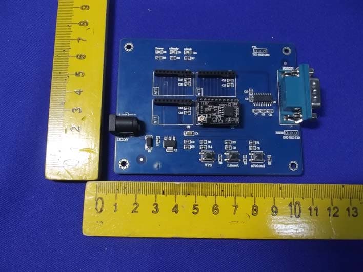
AZY-HF-LPT100
Dec 25, 2013Embedded WiFi Module
Equipment Class
DTS - Digital Transmission System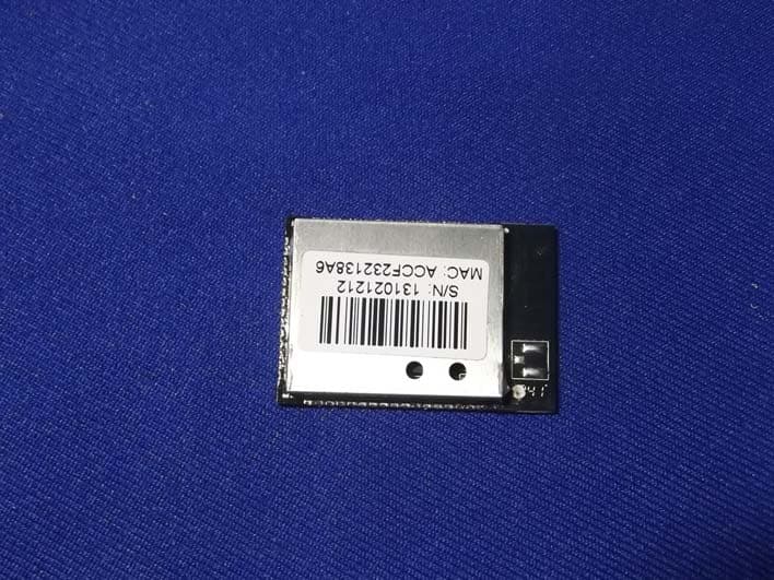
AZY-HF-LPB100
Dec 22, 2013Embedded WiFi Module
Equipment Class
DTS - Digital Transmission System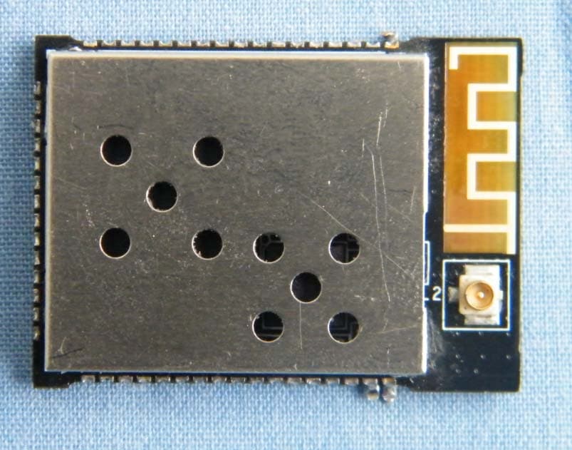
AZY-HF-LPB
Apr 14, 2013Embedded WIFI module
Equipment Class
DTS - Digital Transmission System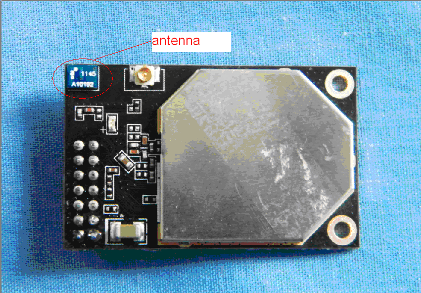
AZYHF-A11X
Mar 22, 2012Embedded WIFI module
Equipment Class
DTS - Digital Transmission System