BCGA1573Apple iBeacon
Apple Inc.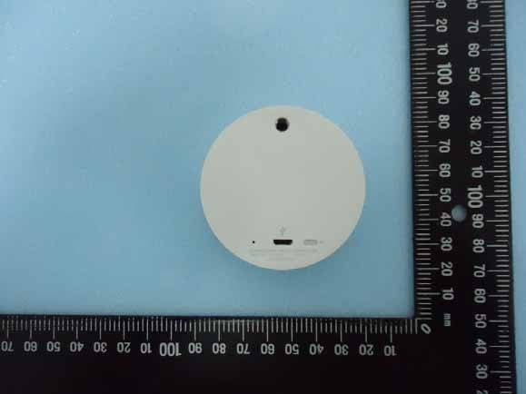
Click to zoom
Application Details
- Equipment Class
- DTS - Digital Transmission System
- Date of Grant
- Jul 03, 2014
- Application Purpose
- Original Equipment
- Date of Application
- Jul 01, 2014
- Equipment Note
- Apple iBeacon
- Frequency Range
- 2402.00000000 - 2480.00000000
- Company
- Apple Inc.
- Country
- United States
Documents & Files
Document Text
Text extracted from the exhibit documents filed with the FCC. Open a document above to read the original.
Users Manual
Apple iBeacon User Guide ReleaseR1 Contents 1. At a Glance5 1.1 Overview 5 1.1.1 ThreadedHole 5 1.1.2 Status LED 5 1.1.3 Micro-USBReceptacle6 1.1.4 Slide Switch 6 1.2 Accessories 6 1.2.1 USB power adapter 6 1.2.2 USB to Micro-USBcable 6 2. GettingStarted7 2.1 Charging 7 2.2 Normal Mode 7 2.3 ProgrammingMode 7 3. Safety, Handling, and Support8 3.1 Handling8 3.2 Repairing 8 3.3 Cleaning8 3.4 Using connectors, ports, and buttons 9 3.5 Charging 9 3.6 Operating temperature 9 3.7 Prolongedheat exposure 9 3.8 Radio frequency interference 10 3.9 Explosive atmospheres 10 4. Regulatory compliance information11 4.1 FCC compliance statement 11 4.2 Canadianregulatory statement 11 4.3 Europe — EU Declaration of Conformity 12 4.4 Japan VCCI Class B Statement 12 5. Disposal and recycling information13 5.1 European Union — Disposal Information 13 2014-07-03 | Copyright © 2014 Apple Inc. All Rights Reserved. 2 5.2 Türkiye 14 5.3 Brasil — Informações sobre descarte e reciclagem14 5.4 Latin America — Informaciónsobre eliminaciónde residuosy reciclaje14 5.5 China — Battery Statement 15 5.6 China — Environmental Protection Information 15 5.7 Taiwan — Battery Statement 15 5.8 Taiwan — Recycling Information 15 5.9 Apple and the environment 16 2014-07-03 | Copyright © 2014 Apple Inc. All Rights Reserved. 3 Contents Tables 1. At a Glance5 Table 1-1Apple iBeacon LED behavior 5 2014-07-03 | Copyright © 2014 Apple Inc. All Rights Reserved. 4 This guide describes Apple iBeacon (Model A1573). 1.1 Overview 1.1.1 ThreadedHole The ThreadedHole (see figure highlight A) accepts a standard M5 screw and may be used to securely mount Apple iBeacon to other structures. 1.1.2 Status LED The Status LED (see figure highlight B) is intendedas a convenient indicator of operating mode and battery state.Undernormaloperatingconditions,theStatusLEDisturnedofftosavepowerandremaininconspicuous. Table 1-1Apple iBeacon LED behavior Fully ChargedChargingNot Charging OffRedOffOff 2014-07-03 | Copyright © 2014 Apple Inc. All Rights Reserved. 5 1. At a Glance Fully ChargedChargingNot Charging OffRedOffNormal Green (Blink)Red/Orange (Blink)GreenProgramming The Status LED will turn off and on at 500 ms intervals when Blink is specifiedalong with a single color. When two colors are specified, the LED will alternate between the two colors every 500 ms instead of between off and on states. 1.1.3 Micro-USBReceptacle Plug a USB to Micro-USBcable into the Micro-USBReceptacle(see figure highlight C) and connect Apple iBeacon into a USB power adapter to charge. 1.1.4 Slide Switch The Slide Switch (see figure highlight D) has 3 possiblepositions: ● Off ● On ● Momentary Apple iBeacon will enter Programmingmode when the Slide Switch is moved from the On positionto the Momentary positionand held there for a minimumof 3 seconds. The Slide Switch may be releasedafter Apple iBeacon has entered this mode. 1.2 Accessories The following accessories are not includedwith Apple iBeacon and must be purchasedseparately: 1.2.1 USB power adapter Use any Apple USB power adapter to power Apple iBeacon and charge the battery. The Apple 5W USB Power Adapter is recommended. 1.2.2 USB to Micro-USBcable Use any standard USB to Micro-USBcable to connect Apple iBeacon to a USB power adapter to charge. 1. At a Glance 1.2 Accessories 2014-07-03 | Copyright © 2014 Apple Inc. All Rights Reserved. 6 2.1 Charging Apple iBeacon has an internal, lithium-ionrechargeablebattery. The best way to charge the Apple iBeacon battery is to connect Apple iBeacon to a power outletusing the not-includedUSB to Micro-USBcable and Apple USB power adapter. 2.2 Normal Mode WhentheSlideSwitchisintheOnposition,theAppleiBeaconwillbevisibletoiOSappsthatworkwithiBeacon, using the configuration that has been set by the Apple iBeacon programmingapp. 2.3 ProgrammingMode To program Apple iBeacon's settings, put the Apple iBeacon into Programmingmode using the Slide Switch and then run the Apple iBeacon programmingapp on anotherApple device. 2014-07-03 | Copyright © 2014 Apple Inc. All Rights Reserved. 7 2. GettingStarted Note: Failure to follow these safety instructions could result in fire, electric shock, or other injuries, or damageto Apple iBeacon or other property. Read all the safety information below before using Apple iBeacon. 3.1 Handling HandleApple iBeacon with care. It is made of plasticand has sensitive electronic components inside. Apple iBeacon can be damagedif dropped, burned, punctured, or crushed, or if it comes in contact with liquid. Don't use a damagedApple iBeacon, such as one with a damagedenclosure, as it may cause injury. 3.2 Repairing Don'topenAppleiBeaconanddon'tattempttorepairAppleiBeaconbyyourself.DisassemblingAppleiBeacon may damageit or may cause injury to you. If Apple iBeacon is damaged, malfunctions, or comes in contact with liquid, contact Apple or an Apple Authorized Service Provider. 3.3 Cleaning Clean Apple iBeacon if it comes in contact with anythingthat might cause stains - such as dirt, ink, makeup, or lotions. To clean: ● Disconnect all cables and turn Apple iBeacon off (slide the Slide Switch to the Off position) ● Use a soft, lint-free cloth ● Avoid gettingmoisture in openings ● Don't use cleaningproducts or compressed air 2014-07-03 | Copyright © 2014 Apple Inc. All Rights Reserved. 8 3. Safety, Handling, and Support 3.4 Using connectors, ports, and buttons Never force a connector into a port or apply excessive pressure to a button, because this may cause damage thatisnotcoveredunderthewarranty.Iftheconnectorandportdon'tjoinwithreasonableease,theyprobably don't match. Check for obstructions and make sure that the connector matches the port and that you have positionedthe connector correctly in relation to the port. 3.5 Charging Charge Apple iBeacon with the USB to Micro-USBcable connected to an Apple USB power adapter (both availableseparately). Using damagedcables or chargers, or charging when moisture is present, can cause electric shock. When you use the Apple USB …
Text truncated - open the document above for the full version.
Cover Letter(s)
Authoritv to Act as Ag:ent Date: 2014-5-21 American Certification Body, Inc. 6731 Whittier A venue Suite C11 0 McLean , VA 22101 To Whom It May Concern: Audix Technology (WuJian旦)Co.、Ltd_._ is authorized to act on our behalf, until otherwise notified, for applications to American Certification Body, Inc. (ACB). We certify that we are not subject to denial offederal benefits , that includes FCC benefits, pursuant to Section 5301 ofthe Anti-Drug Abuse Act of 1988,2 1 U.S.C. 862. Further, no party, as defined in 47 CFR 1.2002 (b),ωthe application is subject to denial offederal benefits, that includes FCC benefits. Thank you , Agency Agreement Expiration Date: 12 months By: 『 e Ricardo David (Print name) Title: Wireless Certification Manal!er On behalf of: Apple Inc. (Company Name) Telephone: 408-996-1010 Appl。 1 Inñnite 1 00ρ ζuperllno.ζ^ 9501,1 1_ Must bc signed by applicant conlact given for applicanl on Ihe FCC sile, or by Ihc aulhorizcd agent ifan阳时卢句古捅l!01Cl 40~ '\.10 uì75 aUlhorizcd agenl Icltcr has becn providcd. Lclters should be placcd on approprialC ICllcrhead.、1 、VViCTJ .applC'.COIII 022311 - 6
Cover Letter(s)
ReQuest for Confidentialitv Date: 2014-5-21 Su时ect:Confidentiality Request for: BCGA1573 PlIrsuant to FCC 47 CRF 0.457( d) and 0.459 and IC RSP-1 00, Section 10, the applicant requests that a part of the subject FCC application be held confidential. Type of Confidentiality Requested 口ShortTerm囚Permanent 囚ShortTerm 2 *ρ 囚S创hort此tT刊erm口m口P阳e创rman阳en川川tμ 口ShortTerm囚Pern町ma 口S仙ho创r忱tT刊erm口Permanent 口S创h阳ort此tT刊erm町mτn口Permanent 口S仙ho创r竹tTerm囚Pern川ma 囚S创h0l1川1Term 因ShortTerm口Permanent* *Note: (Insert Explanation as Necessarv) Exhibit Block D iagrams External Photos Internal Photos Operation Descriptionffheory of Operation Parts List & Placement/BOM Tune-Up Procedllre Schematics Test Setup Photos User's Manual Apple Inc_. __ has spent substantial effort in developing this prodllct and it is one ofthe first of its kind in índustry. Having the sllbject information easily available to "competition" wOllld negate the advantage they have achieved by deve10ping this product. Not protecting the details ofthe design will result in financial hards hip. Pc..mancnt Confidcntiality: The applicant requests the exhibits listed above as pennanently confidential be permanently withheld from public review due to materia ls that contain trade secre ts and proprietary information not customarily released to the public. Short-Term Confidentiality: The applicant requests the exhibits selected above as short term confidential be withheld from public v iew for a period of ~ιdays from the date ofthe Grant of Equipment Authorization and prior to marketing. This is to avoid prema阳rerelease of sensitive information prior to marke ting or re lease of the product to the public. Applicant is also aware that they are responsible to notify ACB in the event information regarding the product or the product is made available to the public. ACB w ill then re lease the docllments listed above for public disclosure pursllant to FCC PlIblic Notice DA 04-1705. NOTE for Industry Canada Applications: The applicant understands that until sllch time that IC distinguishes between Short Tenn and Permanent Confidentiality , either type ofmarked exhibit above w ill simply be marked Confidential when submitted to IC. Sincerely, By: J〈吨 Ricardo David (Print name) 2 _ The asterisked items (ηrequire further justificati on before permanent confidentiality will be allowed. These also currently req uire review by the FCC under their Permit-But-Ask policy before the grant is issued and can delay completion ofan application. Further justification should be added to the note above. One s uc h example for a potted dev ice would be: "The EUT is FULL Y po忧edusing a non-removable epoxy based material. Removal of potting material causes irreparable damage (0 internal c ircuitry. See photographs exhibits that o ut line th e device before and after po忧ing." 3 _ Mu~t be.,í .m:d b\ IppllC3rt con(, ct f;lvcn for appll~ant { 'f' the 1ιζSltιιb> th, auth"l zed 1". 'nt ,1 IpPl{lpriatc 022311- 6 Apple 1 Infmite Looρ ClIpeftino,ι/飞 9',01外 T 408996 11)10 •408 996-02!~ WWW.Jpplt:'.LOO1
Cover Letter(s)
Federal Communications Commission 7435 Oakland Mills Road Columbia MD 21046 Date: July 2, 2014 Subject: Authorized Individual To Whom It May Concern: Pursuant to the provisions of KDB 852134 D01 Authorized Policy Form 731, I, grantee contact, hereby authorize Ricardo David to act on behalf of Apple Inc. for all matters relating to equipment authorization, including signing Form 731, attestations, and confidentiality request letters. This authorization is valid until further written notice from the grantee contact. Marc Douat Apple Inc. 1 Infinite Loop Cupertino, CA 95014
Cover Letter(s)
Federal Communications Commission 7435 Oakland Mills Road Columbia MD 21046 Date: July 2, 2014 Subject: Authorized Individual To Whom It May Concern: Pursuant to the provisions of KDB 852134 D01 Authorized Policy Form 731, I, grantee contact, hereby authorize Ricardo David to act on behalf of Apple Inc. for all matters relating to equipment authorization, including signing Form 731, attestations, and confidentiality request letters. This authorization is valid until further written notice from the grantee contact. Marc Douat Apple Inc. 1 Infinite Loop Cupertino, CA 95014
External Photos
FCC ID: Page 1 of 2 Audix Technology (Wujiang) Co., Ltd. EMC Dept. Report No.: ACWE-F1405007 Figure 1 General Appearance (Front View) Figure 2 General Appearance (Back & Side View & Mini USB Port)
Internal Photos
FCC ID: V7R-TINAVWNA2 Page 1 of 5 Audix Technology (Wujiang) Co., Ltd. EMC Dept. Report No.: ACWE-F1405007 Figure 1 General Appearance (Cover Remove) FIGURE 2 Internal Appearance(PCB Board Remove) FCC ID: V7R-TINAVWNA2 Page 2 of 5 Audix Technology (Wujiang) Co., Ltd. EMC Dept. Report No.: ACWE-F1405007 FIGURE 3 PCB Board (Component Side) FIGURE 4 PCB Board (Solder Side) Antenna Location FCC ID: V7R-TINAVWNA2 Page 3 of 5 Audix Technology (Wujiang) Co., Ltd. EMC Dept. Report No.: ACWE-F1405007 FIGURE 5 PCB Board (Crystal Oscillator) FIGURE 6 PCB Board (Crystal Oscillator) FCC ID: V7R-TINAVWNA2 Page 4 of 5 Audix Technology (Wujiang) Co., Ltd. EMC Dept. Report No.: ACWE-F1405007 FIGURE 7 PCB Board (Component Side) FIGURE 8 PCB Board (Solder Side) FCC ID: V7R-TINAVWNA2 Page 5 of 5 Audix Technology (Wujiang) Co., Ltd. EMC Dept. Report No.: ACWE-F1405007 FIGURE 9 Battery Removed
RF Exposure Info
1.1 Applicable Standard KDB 447498 D01 General RF Exposure Guidance v05 1.2 Specification Limits Limits for General Population/Uncontrolled Exposure Frequency Range (MHz) Electric Field Strength (E) (V/m) Magnetic Field Strength (H) (A/m) Power Density (S) (mW/cm 2 ) Averaging Time |E| 2 , |H| 2 or S (minutes) 0.3-1.34 614 1.63 (100)* 30 1.34-30 824/f 2.19/f (180/f2)* 30 30-300 27.5 0.073 0.2 30 300-1500 -- -- f/150 30 1500-100,000 -- -- 1.0 30 f = frequency in MHz *Plane-wave equivalent power density NOTE: General population/uncontrolled exposures apply in situations in which the general public m ay be exposed, or in which persons that are exposed as a consequence of their employment may not be fully aware of the potential for exposure or can not exercise control over their exposure. The limit value 1.0mW/cm 2 is available for this EUT. 1.3 MPE Calculation Method S = PG/(4πR 2 ) R = [PG/(4πS)] 0.5 where: S = power density (in appropriate units, e.g. mW/ cm 2 ) P = power input to the antenna (in appropriate units, e.g., mW) (the measured power value see Report: F12124 Section 6.6) G = power gain of the antenna in the direction of interest relative to an isotropic radiator R = distance to the center of radiation of the antenna (appropriate units, e.g., cm) 1.4 Calculated Result 2.4.1 Radio Frequency Radiation Exposure Evaluation Frequency Output Power to Antenna Antenna Gain Power Density Limit (MHz) (mW) (dBi) (Numeric)(mW/cm 2 ) (mW/cm 2 ) 240 2 2.55 4.32 2.70 0.00137 1. 24 40 2.87 4.32 2.70 0.00155 1. 2480 3.15 4.32 2.70 0.00169 1. Separation distance R= 20cm. Frequency Output Power to Antenna Antenna Gain Limit Distance (MHz) (mW) (dBi) (Numeric) (mW/cm 2 ) (cm ) 240 2 2.55 4.32 2.70 1.0 0.7405 24 40 2.87 4.32 2.70 1.0 0.7861 2480 3.15 4.32 2.70 1.0 0.8232 The antenna used for this transmitter must be installed to provide a separation distance of at least 0.8232cm from all persons.
Test Report
FCC ID: BCGA1573 Page 1 of 57 Audix Technology (Wujiang )Co., Ltd. EMC Dept. Report No.: ACWE-F1405007 APPLICATION FOR CERTIFICATION On Behalf of Apple Inc. Apple iBeacon Model No. : A1573 Brand : Apple FCC ID : BCGA1573 Prepared for Apple Inc. 1 Infinite Loop, Cupertino, Ca 95014 Prepared by Audix Technology (Wujiang) Co., Ltd. EMC Dept. No. 1289 Jiangxing East Road, the Part of Wujiang Economic Development Zone Jiangsu China 215200 Tel : +86-512-63403993 Fax :+86-512-63403339 Report Number : ACWE-F1405007 Date of Test : Apr.30~May 13, 2014 Date of Report : May 21, 2014 FCC ID: BCGA1573 Page 2 of 57 Audix Technology (Wujiang )Co., Ltd. EMC Dept. Report No.: ACWE-F1405007 TABLE OF CONTENTS Description Page TEST REPORT CERTIFICATION .......................................................................................................4 1. SUMMARY OF MEASUREMENTS AND RESULTS .............................................................5 2. GENERAL INFORMATION.......................................................................................................6 2.1. Description of Device (EUT).................................................................................................................. 6 2.2. Description of Test Facility .................................................................................................................... 7 2.3. Measurement Uncertainty....................................................................................................................... 7 3. CONDUCTED EMISSION MEASUREMET ............................................................................8 3.1. Test Equipment ....................................................................................................................................... 8 3.2. Block Diagram of Test Setup.................................................................................................................. 8 3.3. Power line Conducted Emission Limit ................................................................................................... 8 3.4. Test Procedure ........................................................................................................................................ 9 3.5. Conducted Emission Measurement Results............................................................................................ 9 4. RADIATED EMISSION MEASUREMENT ............................................................................16 4.1. Test Equipment ..................................................................................................................................... 16 4.2. Block Diagram of Test Setup................................................................................................................ 16 4.3. Radiated Emission Limits ..................................................................................................................... 18 4.4. Test Procedure ...................................................................................................................................... 18 4.5. Assessment In All Three Orthogonal Planes ........................................................................................ 19 4.6. Measurement Results ............................................................................................................................ 20 4.7. Restricted Bands Measurement Results (For Below 1GHz)................................................................. 21 4.8. Restricted Bands Measurement Results (For Above 1GHz) ................................................................ 25 4.9. Spurious Emission Measurement Results in Band Edge Emission (FCC Part 15, 15.205).................. 29 5. 6 DB BANDWIDTH MEASUREMENT ...................................................................................37 5.1. Test Equipment ..................................................................................................................................... 37 5.2. Block Diagram of Test Setup................................................................................................................ 37 5.3. Specification Limits (§15.247(a)(2)) .................................................................................................... 37 5.4. Test Procedure ...................................................................................................................................... 37 5.5. Test Results........................................................................................................................................... 37 6. MAXIMUM PEAK OUTPUT POWER MEASUREMENT ...................................................40 6.1. Test Equipment ..................................................................................................................................... 40 6.2. Block Diagram of Test Setup................................................................................................................ 40 6.3. Specification Limits (§15.247(b)(3)) .................................................................................................... 40 6.4. Test Procedure ...................................................................................................................................... 40 6.5. Test Results........................................................................................................................................... 40 7. BAND EDGES MEASUREMENT ............................................................................................41 7.1. Test Equipment ..................................................................................................................................... 41 7.2. Block Diagram of Test Setup................................................................................................................ 41 7.3. Specification Limits (§15.247(d)).....................…
Text truncated - open the document above for the full version.
Test Setup Photos
FCC ID: Page 1 of 4 Audix Technology (Wujiang) Co., Ltd. EMC Dept. Report No.: ACWE-F1405007 1. PHOTOGRAPHS 1.1. Conducted Emission Measurement Front View of conducted emission measurement Side View of conducted emission measurement FCC ID: Page 2 of 4 Audix Technology (Wujiang) Co., Ltd. EMC Dept. Report No.: ACWE-F1405007 1.1.1. For Restricted Bands FCC ID: Page 3 of 4 Audix Technology (Wujiang) Co., Ltd. EMC Dept. Report No.: ACWE-F1405007 1.1.2. For Restricted Bands and Band Edge Emission FCC ID: Page 4 of 4 Audix Technology (Wujiang) Co., Ltd. EMC Dept. Report No.: ACWE-F1405007 1.2. Photo of Section 5,6, 7, 8
Contact Information
Applicant
Abhishek Rala(Regulatory Compliance Manager)
Technical Contact
Audix Technology (Wujiang) Co., Ltd.Jingo Lin
[email protected]+86-512-63403993
No. 1289, JiangXing East Road, The Eastern Part of · Wujiang · China
Non-Technical Contact
Audix Technology (Wujiang) Co., Ltd.Ken Lu
[email protected]+86-512-63403993
Test Firm
Audix Technology(WuJiang)Co.,LtdAllen Wang
Technical Specifications
| # | Rule Parts | Frequency Range | Power Output |
|---|---|---|---|
| 1 | 15C | 2.40 GHz - 2.48 GHz | 3.15 mW |
Other Applications from Apple Inc.
BCG-E9204A
Sep 09, 2026Smartphone
Equipment Class
6VL - 15E 6 GHZ Very Low Power DeviceBCGA3277
Sep 09, 2026Magnetic Charging Cable
Equipment Class
DCD - Part 15 Low Power Transmitter Below 1705 kHzBCGA3641
Sep 09, 2026Magnetic Charger
Equipment Class
DCD - Part 15 Low Power Transmitter Below 1705 kHzBCGA3669
Sep 09, 2026Magnetic Charger
Equipment Class
DCD - Part 15 Low Power Transmitter Below 1705 kHzBCG-E9193A
Sep 09, 2026Smartphone
Equipment Class
PCE - PCS Licensed Transmitter held to ear