BEJ-F1DA2835PBluetooth module
LG Electronics USA, Inc.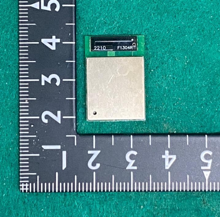
Click to zoom
Application Details
- Equipment Class
- DTS - Digital Transmission System
- Date of Grant
- Nov 07, 2023
- Application Purpose
- Original Equipment
- Date of Application
- Nov 07, 2023
- Equipment Note
- Bluetooth module
- Frequency Range
- 2402.00000000 - 2480.00000000
- Company
- LG Electronics USA, Inc.
- Country
- United States
Documents & Files
Document Text
Text extracted from the exhibit documents filed with the FCC. Open a document above to read the original.
Users Manual
F1DA2835P Datasheet Confidential / Preliminary Documentation Revision 1.3 List of Contents 1. General 1.1 Overview 1.2 Features 1.3 Application 1.4 Pinout Diagram 1.5 Device Terminal Functions 1.6 Module Dimension 2. Characteristics 2.1 Electrical Characteristics 2.2 RF Characteristics 2.3 Audio Characteristics 3. Interface 3.1 USB 3.2 I2C 3.3 UART0 and UART1 3.4 SPI 3.5 PWM 3.6 Audio Interfaces 4. Application Schematic 5. Antenna Spec 6. Module Placement Rule 7. PCB Layout 8. Reflow Temperature Profile 9. Packing Information 10. Revision History 1. General 1.1 Overview This specification covers Bluetooth module which complies with Bluetooth specification version 5.3 and integrates RF & Baseband controller in small package. This Module has deployed Action’s ATS2835P Chipset 1.2 Features • Bluetooth supports . Support Bluetooth V5.3 . Compatible with Bluetooth V5.2/V5.0/V4.2/V4.2 LE/V4.0/V3.0/V2.1 + EDR . RF performance of 5dbm Transmitter power . -93dBm@GFSK, -92dBm@π/4 DQPSK, -87dBm@8DPSK modulation. . Internal Chip Antenna • 342MHz CEVA TL420 DSP core • Audio Interface . I2S TX and I2S RX*2, sampling rate up to 192KHz . SPDIF TX and RX, sampling rate up to 96KHz . Analog and Digital microphone • Physical interfaces . Supports SD/MMC/eMMC card interface . Supports SDIO interface . USB 2.0 device and host controllers . Serial Interface: SPI*2, UART*2, I2C . Supports Remote Control with internal IRC . Supports LCM with 8bit CPU Interface, 4COM/5COM/6COM Segment LCD, 7pin LED . 9 PWM drivers independent of MCU . Supports 32 GPIO and 1 WIO(wake up IO) • Memory . Internal 32M bits SPI serial Flash for custom defined software . Internal 498.5KB RAM . Internal 32KB CPU ICache for SPI NorFlash . Internal 32KB Cache for SPI pSRAM • Improved Audio Quality . SBC & AAC Bluetooth audio transmission format . Stereo Codec 1.3 Application • Portable stereo speakers • Bluetooth car audio unit • Stereo headsets and headphones • Other Bluetooth audio applications • Speaker phones 1.4 Pinout Diagram 1.5 Device Terminal Functions Pin No. Pin Name Function Multiplex IO Type PAD Drive Level GPI O Initi al Stat e Description 1 GPIO0 /I2C_CLK LED_COM0 LCD_WRB LCD_COM0 PWM1 UART0_RTS I2STX_MCLK I2SRX0_MCLK I2SRX1_MCLK Timer2_cap SPI2_SS DIO 2/4/6/8/10/ 12/14/16mA Z Bit0 of General purpose I/O port 2 GPIO2 LED_COM2 LCD_RDB LCD_COM2 SPI1_MOSI PWM2 UART0_RX LRADC4 I2STX_LRCLK I2SRX0_LRCLK I2SRX1_LRCLK Timer2_cap SPI2_MOSI DIO 2/4/6/8/10/ 12/14/16mA V Bit2 of General purpose I/O port 3 GPIO1 LED_COM1 LCD_RS LCD_COM1 I2C_SDA PWM3 UART0_CTS I2STX_BCLK I2SRX0_BCLK I2SRX1_BCLK Timer3_cap SPI2_MISO DIO 2/4/6/8/10/ 12/14/16mA Z Bit1 of General purpose I/O port 4 GPIO3 LED_COM3 LCD_CEB LCD_COM3 SPI1_CLK UART0_TX I2STX_DOUT I2SRX0_DIN I2SRX1_DIN Timer3_cap SPI2_CLK DIO 2/4/6/8/10/ 12/14/16mA V Bit3 of General purpose I/O port 5 GPIO19 LCD_SEG17 I2C_SDA Timer3_cap DIO 2/4/6/8/10/ 12/14/16mA Z Bit19 of General purpose I/O port 6 RTC_VDD PWR RTC power 7 ON_OFF AI ON/OFF reset signal 8 GND GND GND 9 VBAT PWR Battery Voltage input 10 DC_5V PWR 5.0V Voltage 11 VCC PWR Digital IO PWR 12 WIO0 LRADC1 DIO 2/4/6/8/10/ 12/14/16mA WIO 0 LRADC1 13 SVCC PWR PWR for standby 14 AVCC PWR Analog IO PWR 15 AGND GND Analog GND 16 GPIO[7] /I2S_DIN LED_COM7 PTA_GRANT LCD_SEG1 SPDIF_RX PWM0 UART1_TX FMCLKOUT I2STX_DOUT I2SRX1_DIN Timer3_cap SD1_DAT3 DIO 2/4/6/8/10/ 12/14/16mA Z Bit7 of General purpose I/O port 17 GPIO[4] /HOST_EN LED_COM4 LCD_CEB LCD_COM4 PWM1 Timer2_cap IR_RX DIO 2/4/6/8/10/ 12/14/16mA Z Bit4 of General purpose I/O port 18 AUX_1R GPIO49 AI/DIO 2/4/6/8/10/ 12/14/16mA Linein right channel input1 19 AUX_1L GPIO48 AI/DIO 2/4/6/8/10/ 12/14/16mA Linein left channel input1 20 AUX_0R GPIO47 AI/DIO 2/4/6/8/10/ 12/14/16mA Linein right channel input0 21 AUX_0L GPIO46 AI/DIO 2/4/6/8/10/ 12/14/16mA Linein left channel input0 22 AUX_2R GPIO55 AI/DIO 2/4/6/8/10/ 12/14/16mA Linein right channel input2 23 AUX_2L GPIO54 AI/DIO 2/4/6/8/10/ 12/14/16mA Linein left channel input2 24 MIC_NR GPIO45 DMIC_DAT AI/DIO 2/4/6/8/10/ 12/14/16mA Microphone right channel input 25 MIC_NL GPIO44 DMIC_CLK AI/DIO 2/4/6/8/10/ 12/14/16mA Microphone left channel input 26 AOUT_LN GPIO51 I2STX_LRCLK I2SRX0_LRCLK I2SRX1_LRCLK PWM3 AO/DIO 2/4/6/8/10/ 12/14/16mA Left channel differential output 27 AOUT_L GPIO50 AO/DIO 2/4/6/8/10/ 12/14/16mA Left channel output 28 AOUT_R GPIO52 AO/DIO 2/4/6/8/10/ 12/14/16mA Right channel output 29 AOUT_RN GPIO53 I2STX_DOUT AO/DIO 2/4/6/8/10/ 12/14/16mA Right channel differential output I2SRX0_DIN I2SRX1_DIN PWM5 30 AGND GND Analog Ground 31 GND GND GND 32 USB_DM AIO USB Data minus 33 USB_DP AIO USB Data plus 34 GPIO[17] /SD_CLK SPI2_CLK LCD_SEG15 SPI1_CLK UART0_TX Timer3_cap DIO 2/4/6/8/10/ 12/14/16mA Z Bit17 of General purpose I/O port 35 GPIO[20] /SD_DAT SPI2_MISO LCD_D8 LCD_SEG10 SPI1_MISO PWM2 UART1_CTS Timer2_cap DIO 2/4/6/8/10/ 12/14/16mA Z Bit20 of General purpose I/O port 36 GPIO[38] /I2S_DOU T SPDIF_RX BT_REQ LCD_SEG28 PWM0 I2SRX0_DIN I2SRX1_DIN DIO 2/4/6/8/10/ 12/14/16mA PU Bit38 of General purpose I/O port 37 GPIO[39] /I2S_BCLK BT_ACCESS LCD_SEG29 PWM1 I2SRX0_BCLK I2SRX1_BCL K DIO 2/4/6/8/10/ 12/14/16mA PU Bit39 of General purpose I/O port 38 GPIO[40] /I2S_MCL K PTA_GRANT LCD_SEG30 PWM2 I2SRX0_MCLK I2SRX1_MCL K DIO 2/4/6/8/10/ 12/14/16mA PU Bit40 of General purpose I/O port 39 GPIO[5] /PA_CTL2 LED_COM5 BT_REQ LCD_COM5 PWM3 Timer3_cap DIO 2/4/6/8/10/ 12/14/16mA Z Bit5 of General purpose I/O port 40 GPIO[21] /PA_CTL1 SPI2_MOSI LCD_D9 LCD_SEG11 SPI1_MOSI PWM0 UART0_RX TEMPADC I2STX_MCLK I2SRX0_MCLK I2SRX1_MCLK Timer3_cap SD1_CLK UART1_TX SD0_DAT1 DIO 2/4/6/8/10/ 12/14/16mA Z Bit21 of General purpose I/O port 41 GPIO[6] /I2S_LRCL K LED_COM6 BT_ACCESS LCD_SEG0 PWM4 I2SRX0_LRCLK I2SRX1_LRCLK Timer2_cap SD1_DAT0 DIO 2/4/6/8/10/ 12/14/16mA Z Bit6 of General purpose I/O port 42 GPIO[23] /SPDIF_TX LCD_D11 LCD_SEG13 PWM2 UART0_TX LRADC3 I2STX_BCLK I2SRX0_BCLK I2SRX1_BCLK Timer3_cap SD1_CMD SD0_DAT3 SD0_DAT0 DIO 2/4/6/8/10/ 12/14/16mA Z Bit23 …
Text truncated - open the document above for the full version.
Attestation Statements
LG Electronics USA, Inc. Covered Equipment Certification Attestation Letter DATE Nemko North America, Inc. 303 River Road Ottawa K1V 1H2 Canada ATTN.: Reviewing Engineer FCC ID: BEJ-F1DA2835P LG Electronics USA, Inc. (“the applicant”) certifies that the equipment for which authorization is sought is not “covered” equipment prohibited from receiving an equipment authorization pursuant to section 2.903 of the FCC rules. Note: If the equipment for which the applicant seeks authorization is produced by any of the entities identified on the current Covered List, the applicant should include an explanation on why the equipment is not “covered” equipment. LG Electronics USA, Inc.. (“the applicant”) certifies that, as of the date of the filing of the application, the applicant is not identified on the Covered List as an entity producing “covered” equipment. Signed: Printed name: Heejae Cho Title: Director, Regulatory and Environmental Affairs Company Name: LG Electronics USA, Inc. Date: 9/7/2023
Attestation Statements
LG Electronics USA, Inc. * the applicant must designate a contact located in the United States for purposes of acting as the applicant’s agent for service of process, regardless of whether the applicant is a domestic or foreign entity. An applicant located in the United States may designate itself as the agent for service of process. U.S. Agent Designation for Service of Process - Certification Attestation Letter September 26, 2023 Nemko North America, Inc. 303 River Road Ottawa K1V 1H2 Canada ATTN.: Reviewing Engineer FCC ID: BEJ-F1DA2835P Per section 2.911(d)(7) of the FCC rules, LG Electronics Inc.(“the applicant”) certifies that the equipment for which authorization is sought is designated to the following U.S. Designated agent* for service of process: Company Name: LG Electronics USA, Inc. Physical U.S. Company Address: 111 Sylvan Avenue North Building, Englewood Cliffs, NJ 07632 Agent name: Heejae Cho Agent Email Address: [email protected] FRN: 0017130477 The above contact person accepts the obligation for service of process. The applicant accepts to maintain an agent for no less than one year after the grantee has terminated all marketing and importation or the conclusion of any Commission-related proceeding involving the equipment. Applicant Signed: Designated Agent Signed: (Required, if different to Applicant): Signed: Signed: Printed name: Heejae Cho Printed name: Click here to enter text. Title: Director, Regulatory and Environmental Affairs Title: Click here to enter text. Company Name: LG Electronics USA, Inc. Company Name: Click here to enter text. Date: September 7, 2023 Date: Click here to enter a date.
Cover Letter(s)
LG Electronics USA, Inc. 9/26/2023 Nemko North America, Inc. 303 River Road Ottawa, Ontario, Canada K1V 1H2 AUTHORITY TO ACT AS AGENT - FCC On our behalf, I appoint Nemko Korea Co., Ltd (165-51, Yurim-ro, Cheoin-gu, Yongin-si, Gyeonggi-do, 17042, Korea), to act as our agent in the preparation of this application for equipment certification. I certify that submitted documents properly describe the device or system for which equipment certification is sought. I also certify that each unit manufactured, imported or marketed, as defined in FCC regulations will have affixed to it a label identical to that submitted for approval with this application. In signing this letter, Applicant certifies that neither the applicant nor any party to the application is not subject to a denial of Federal benefits, that include FCC benefits, pursuant to Section 5301 of the Anti-Drug Abuse Act of 1988, 21 U.S.C. § 862 because of a conviction for possession or distribution of a controlled substance. See 47 CFR 1.2002(b) for the definition of a "party" for these purposes. For instances where our authorized agent signs the application for certification on our behalf, I acknowledge that all responsibility for complying with the terms and conditions for certification, as specified by Nemko North America Inc., still resides still resides with us. Sincerely, Printed name: Heejae Cho
Cover Letter(s)
LG Electronics USA, Inc. September 26, 2023 Nemko North America, Inc. 303 River Road Ottawa, Ontario, Canada K1V 1H2 REQUEST FOR CONFIDENTIALITY - FCC FCC ID: BEJ-F1DA2835P Pursuant to Sections 0.457(d) and 0.459 of the Commission’s Rules and FCC Guidance document 726920, we hereby request permanent confidential treatment of exhibits identified as such in the table below and request they are permanently withheld from public review based on the documents containing trade secrets and proprietary information not customarily released to the public. The public disclosure of this information might be harmful to the applicant and provide unjustified benefits to its competitors. We also request short-term confidentiality on certain exhibits until the intended date of marketing as outlined below. We request the exhibits be withheld from public view for a period of 180 days. We attest marketing of the product will only commence after the period of short-term confidentiality expires, or if marketing is to commence before the requested number of days listed above, the grantee will inform Nemko to release the Short-Term Confidentiality information withheld on the FCC equipment authorization website. Exhibit Type of Confidentiality Requested Block Diagrams ☒ Permanent ☐ Short Term External Photos ------------------ ☒ Short Term Internal Photos ☐ Permanent* ☒ Short Term Operation Description ☒ Permanent ☐ Short Term Parts List & Placement/BOM ☒ Permanent ☐ Short Term Tune-Up Procedure ☒ Permanent ☐ Short Term Schematic Diagrams ☒ Permanent ☐ Short Term Test Setup Photos ------------------ ☒ Short Term User’s Manual ☐ Permanent* ☒ Short Term The asterisked items (*) require further information to be provided in this justification letter before permanent confidentiality will be extended to these exhibits. Please refer to FCC KDB 726920 D01 found at: https://apps.fcc.gov/oetcf/kdb/forms/FTSSearchResultPage.cfm?switch=P&id=41731 and review section II, 3) regarding specific information that must accompany these requests. Note: any documents held under the Short-Term confidentiality will automatically become public after the requested time if an appropriate extension request has not been received. Any exhibits (i.e., schematic diagrams) that may have already been requested to have “Permanent” confidentiality as shown above need not be repeated under Short-Term confidentiality request. Sincerely, Signed: Printed name: Heejae Cho Title: Director, Regulatory and Environmental Affairs Company Name: LG Electronics USA, Inc.
Cover Letter(s)
LG Electronics USA, Inc. September 14, 2023 Federal Communications Commission Equipment Authorization Branch 7435 Oakland Mills Road Columbia, MD 21046 Modular Approval Request FCC ID: BEJ-F1DA2835P The following attestation addresses the requirements to support modular approval: Modular approval requirement Yes (provide brief statement) No * (a) The radio elements must have the radio frequency circuitry shielded. Physical components and tuning capacitor(s) may be located external to the shield, but must be on the module assembly The device is equipped with Metal shielding to cover RF section. Refer to the external photos (b) The module must have buffered modulation/data inputs to ensure that the device will comply with Part 15 requirements with any type of input signal All inputs to the modules are buffered through logic or microprocessor inputs. (c) The module must contain power supply regulation on the module Power supply regulation built into module. Refer to the circuit diagram. (d) The module must contain a permanently attached antenna, or contain a unique antenna connector, and be marketed and operated only with specific antenna(s), per Sections 15.203, 15.204(b), 15.204(c), 15.212(a), 2.929(b) Connector is unique. (e) The module must demonstrate compliance in a stand-alone configuration Refer to the test report and setup photo. (f) The module must be labelled with its permanently affixed FCC ID label, or use an electronic display (See KDB Publication 784748 about labelling requirements) Label is to be placed on front of the EUT, and other label is to be placed in the User Manual. Refer to the FCC ID label format. (g) The module must comply with all specific rules applicable to the transmitter. The grantee must provide comprehensive instructions to explain compliance requirements Refer to the User manual Modular approval requirement Yes (provide brief statement) No * (h) The module must comply with RF exposure requirements It complies with RF exposure requirement. * Please provide a detailed explanation if the answer is “No.” Sincerely, Signed: Printed name: Heejae Cho Title: Director, Regulatory and Environmental Affairs
External Photos
Project No.: NK-23-R-231 FCC and IC Certification FCC ID: BEJ-F1DA2835P / IC : 2703H-F1DA2835P Page 1 of 1 External Photo Front View of EUT Rear View of EUT
ID Label/Location Info
FCC and IC Certification FCC ID : BEJ-F1DA2835P / IC : 2703H-F1DA2835P Page 1 of 1 LABELLING REQUIREMENTS The sample label shown shall be permanently affixed at a conspicuous location on the device and be readily visible to the user at the time of purchase. [Top] Labelling Requirements
Internal Photos
Project No.: NK-23-R-231 FCC and IC Certification FCC ID: BEJ-F1DA2835P / IC : 2703H-F1DA2835P Page 1 of 2 Internal Photo Front View of Main Board Rear View of Main Board Project No.: NK-23-R-231 FCC and IC Certification FCC ID: BEJ-F1DA2835P / IC : 2703H-F1DA2835P Page 2 of 2 Internal Photo View of Antenna
RF Exposure Info
September 19, 2023 Project No.: NK-23-R-231 FCC Certification LG Electronics USA., Inc. FCC ID : BEJ-F1DA2835P Page 1 of 2 Maximum Permissible Exposure RF Exposure Limit According to FCC 1.1310: The criteria listed in the following table shall be used to evaluate the Environmental of human exposure to radio frequency (RF) radiation as specified in 1.1307(b) Limits for Maximum Permissible Exposure (MPE) Frequency Electric Field Magnetic Field Power Density Averaging Time Range(MHz) Strength(V/m) Strength(A/m) (mW/cm 2 ) (Minutes) 30 - 300 61.4 0.163 1 6 300 - 1500 ... ... F/300 6 1500 - 100000 ... ... 5 6 30 - 300 27.5 0.073 0.2 30 300 - 1500 ... ... F/1500 30 1500 - 100000 ... ... 1 30 (A) Limits for occupational / Contral Exposure (B) Limits for General Population / Uncontrolled Exposure F = Frequency (MHz) Fries formula Fries transmission formula : Pd = (Pout * G) / (4 * π* r²) r = √((Pout * G) / 4 * π* Pd)) Where Pd = Power density in ㎽/㎠ Pout = Output power to antenna in ㎽ G = Gain of antenna in linear scale π= 3.1416 r = Distance between observation point center of the radiator in cm Pd is the limit of MPE, 1㎽/㎠. If we know the Maximum Gain of the antenna and the total power input to the antenna, through the calculation, we will know the Maximum distance r where the MPE limit is reached and Power density at prediction frequency. September 19, 2023 Project No.: NK-23-R-231 FCC Certification LG Electronics USA., Inc. FCC ID : BEJ-F1DA2835P Page 2 of 2 Maximum Permissible Exposure Test Result : The maximum antenna gain is 2.1 dBi or 1.62(Numeric). Max. power with turn-up tolerance: 7.00 (dBm) Max. power with turn-up tolerance: 5.01 (mW) Antenna gain(Peak): 2.10 (dBi) Maximum antenna gain: 1.62 (numeric) Prediction distance: 20 (cm) Prediction frequency: 2402 (MHz) MPE limit for uncontrolled exposure at prediction frequency: 1 (mW/cm^2) Power density at prediction frequency : 0.001617 (mW/cm^2) Test result: PASS
Test Report
1 / 12 F1media 2.4GHz SMD Antenna F1304R 1. Features • Designed for 2.4GHz applications: BT / BLE, Wi-Fi ® (802.11/b/g/n), ZigBee ® , etc. • Easy to integrate • Low profile design • High efficiency • Intended for SMD mounting • Supplied in tape and reel 2. Description F1-FR4-ANT is intended for use with all 2.4 GHz applications. The antenna uses a ground plane in order to radiate efficiently, but this ground plane must not extend underneath the antenna itself. 3. Applications • Wearables • Notebooks • PC-cards • Sensors 2 / 12 F1media 2.4GHz SMD Antenna F1304R 4. Part Number F1-FR4-ANT : F1304R 5. General Data Product name F1-FR4 ANT Part Number F1304R Frequency 2.4 – 2.5GHz Polarization Linear Operating temperature -40°C to 140°C Environmental condition test ISO 16750-4.5.1.1.1/5.1.2.1/5.3.2 Impedance with matching 50Ω Weight 0.1g Antenna type SMD Dimensions 12.8 X 3.9 X 1.1 (mm) 6. RF Characteristics 2.4-2.5GHz Conditions Peak gain 2.1 dBi All data measured on F1-media’s evaluation PCB, part no. F1304R-EVB-1 Average gain (Linear) -1.2 dBi Average efficiency 75% Maximum return loss -11 dB Maximum VSWR 1.8:1 Antennas for Wireless Applications 3 / 12 F1media 2.4GHz SMD Antenna F1304R 7. RF Performance 7.1 Return Loss 7.2 VSWR 4 / 12 F1media 2.4GHz SMD Antenna F1304R 7.3 Antenna pattern 7.3.1 2400 MHz – 2500 MHz 3D pattern at 2450 MHz Drag to rotate pattern and PCB by using Adobe Reader (Click to Activate) Antennas for Wireless Applications 5 / 12 F1media 2.4GHz SMD Antenna F1304R 8. Antenna Dimensions F1-FR4-ANT: F1304R Top side Bottom Side 5 solder pads (2.0 x 1.0 mm) All Dimensions in (mm) 6 / 12 F1media 2.4GHz SMD Antenna F1304R 9. Schematic symbol and Pin definition The circuit symbol for the antenna is shown below. The antenna has 5 pins with only two as functional. All other pins are for mechanical strength. 10. Antenna footprint for Wi Pin Description 2 Feed 3 GND 1,4,5 Not used (Mechanical only) I S K J N L O 1.0±0.1 20.±0.1 8.1±0.1 3.7±0.1 1.3±0.1 2.4±0.1 0.5±0.1 7 / 12 F1media 2.4GHz SMD Antenna F1304R 11. Electrical Interface 11.1 Transmission Line All transmission lines should be designed to have a characteristic impedance of 50Ω. • The length of the transmission lines should be kept to a minimum • Any other parts of the RF system like transceivers, power amplifiers, etc, should also be designed to have an impedance of 50 Ω Once the material for the PCB has been chosen (PCB thickness and dielectric constant), a coplanar transmission line can easily be designed using any of the commercial software packages for transmission line design. For the chosen PCB thickness, copper thickness and substrate dielectric constant, the program will calculate the appropriate transmission line width and gaps on either side of the track, so the characteristic impedance of the co-planar transmission is 50 Ω. 11.2 Matching Circuit The antenna requires a matching circuit that must be optimized for each customer’s product. The matching circuit will require up to three components and the following pad layout should be designed into the device so the correct circuit can be installed: The antenna feed pad and the antenna ground pad are indicated in the drawing above. Additional pads are for mechanical attachment only and should not be grounded. 8 / 12 F1media 2.4GHz SMD Antenna F1304R 12. Antenna Integration Guide 12.1 Antenna Placement F1media M2M strongly recommends placing the antenna at the edge of the board. Maximum antenna performance is achieved by placing the antenna towards one of the corners of the PCB and with the feed point of the antenna as close to same corner of the PCB as possible. Additional ground and components near the antenna should be at a distance of at least 2mm. Where possible the antenna should be clear of ground from both sides, although the antenna can work well with a minimum clearance of D ≥ 2 mm as shown in the drawing above. 9 / 12 F1media 2.4GHz SMD Antenna F1304R 13. Reference Board The reference board has been designed for evaluation of F1304R and they include a SMA female connector. Dimensions in mm 10 / 12 F1media 2.4GHz SMD Antenna F1304R 14. Reference Board Matching Circuit 15. Soldering This antenna is suitable for lead free soldering. The reflow profile should be adjusted to suit the device, oven, and solder paste, while observing the following conditions: • The maximum temperature should not exceed 240 ºC • However, for lead free soldering, a maximum temperature of 255 ºC for no more than 20 seconds is permitted. • The antenna should not be exposed to temperatures exceeding 120 ºC more than 3 times during the soldering process. Designator Type Value Description L1 Inductor 15nH Murata LQG15HN series C1 Capacitor 2.2pF Murata GJM15 series C2 Capacitor Not fitted Not fitted 11 / 12 F1media 2.4GHz SMD Antenna F1304R 16. Packaging 16.1 Optimal Storage Conditions Temperature -10ºC to 40ºC Humidity Less than 75% RH Shelf life 24 Months Storage place Away from corrosive gas and direct sunlight Packaging Reels should be stored in unopened sealed manufacturer’s plastic packaging. Note: Storage of open reels of antennas is not recommended due to possible oxidization of pads on antennas. If short term storage is necessary, then it is highly recommended that the bag containing the antenna reel is re-sealed and stored in like storage conditions as in above table. 12 / 12 F1media 2.4GHz SMD Antenna F1304R 17. Revision History Revision Date Change Descriptions Issued by Rev 1.0 2020-01-08 Initial release T.G KIM
Test Report
Test Report No.: REP015887-2 FCC ID: BEJ-F1DA2835P TRF-FCC&IC-RF_Rev.0.1 Nemko Korea Co., Ltd. Page 1 of 49 Nemko Korea Co., Ltd. 165-51, Yurim-ro, Cheoin-gu, Yongin-si, Gyeonggi-do, 17042, Republic of Korea. TEL :+82 31 330-1700 FAX:+82 31 322 2332 FCC EVALUATION REPORT FOR CERTIFICATION Project No. : NK-23-R-231 Dates of receipt : July 24, 2023 Applicant : LG Electronics USA., Inc. Dates of Issue : September 26, 2023 27, Digital-ro 27 ga-gil, Guro-gu SEOUL 08375, Korea, Republic of Attn. : Byeong-Seob Lee Test Site : Nemko Korea Co., Ltd. Model: F1DA2835P Additional Model(s): - EUT Type: Bluetooth module Classification: Digital Transmission Systems (DTS) Date of Test: July 27, 2023 ~ September 05, 2023 Applied Standard: FCC 47 CFR Part 15.247 The device bearing the brand name and model specified above has been shown to comply with the applicable technical standards as indicated in the measurement report and was tested in accordance with the measurement procedures specified in ANSI C63.10-2013. The client should not use it to claim product endorsement by TAF or any government agencies. The test results in the report only apply to the tested sample. I attest to the accuracy of data and all measurements reported herein were performed by me or were made under my supervision and are correct to the best of my knowledge and belief. I assume full responsibility for the completeness of these measurements and vouch for the qualifications of all persons taking them. Tested By : Hyeonseung Lee Reviewed By : Hoonpyo Lee Test Engineer Technical Manager FCC ID: BEJ-F1DA2835P Applicant : LG Electronics USA., Inc. Brand Name LG Test Report No.: REP015887-2 FCC ID: BEJ-F1DA2835P TRF-FCC&IC-RF_Rev.0.1 Nemko Korea Co., Ltd. Page 2 of 49 Revision History Rev. Issue Date Revisions Revised By 00 September 26, 2023 Initial issue Hyeonseung Lee Test Report No.: REP015887-2 FCC ID: BEJ-F1DA2835P TRF-FCC&IC-RF_Rev.0.1 Nemko Korea Co., Ltd. Page 3 of 49 TABLE OF CONTENTS 1. INTRODUCTION ............................................................................................................................... 4 1.1 Test facility ....................................................................................................................................................... 4 1.2 Accreditation and listing ................................................................................................................................... 4 2. EUT INFORMATION & TEST CONDITIONS .................................................................................... 5 2.1 EUT Information ............................................................................................................................................... 5 2.2 Operation During Test ...................................................................................................................................... 6 2.3 Support Equipment .......................................................................................................................................... 9 2.4 Setup Drawing .................................................................................................................................................. 9 3. ANTENNA REQUIREMENTS ......................................................................................................... 10 4. SUMMARY OF TEST RESULTS .................................................................................................... 11 5. TEST METHODOLOGY .................................................................................................................. 11 6. DESCRIPTION OF TESTS .............................................................................................................. 12 6.1 Duty Cycle ...................................................................................................................................................... 12 6.2 6 dB Bandwidth / Occupied Bandwidth .......................................................................................................... 13 6.3 Peak Output Power ........................................................................................................................................ 14 6.4 Power Spectral Density .................................................................................................................................. 15 6.5 Band Edge / Conducted Spurious Emissions ................................................................................................ 16 6.6 Radiated Emissions ....................................................................................................................................... 17 6.7 AC Line Conducted Emissions....................................................................................................................... 18 7. TEST DATA .................................................................................................................................... 19 7.1 Duty Cycle ...................................................................................................................................................... 19 7.2 6 dB Bandwidth .............................................................................................................................................. 21 7.3 Peak Output Power ........................................................................................................................................ 24 7.4 Power Spectral Density .................................................................................................................................. 27 7.5 Band Edge / Conducted Spurious Emissions ................................................................................................ 30 7.6 Radiated Spurious Emissions ........................................................................................................................ 35 7.7 R…
Text truncated - open the document above for the full version.
Test Setup Photos
Project No.: NK-23-R-231 FCC and IC Certification FCC ID : BEJ-F1DA2835P / IC : 2703H-F1DA2835P Page 1 of 6 PHOTOGRAPHS OF TEST SET-UP Test Picture show the worst-case configuration and cable placement. Radiated Test_Below 1 GHz_Front Radiated Test_Below 1 GHz_Rear Project No.: NK-23-R-231 FCC and IC Certification FCC ID : BEJ-F1DA2835P / IC : 2703H-F1DA2835P Page 2 of 6 PHOTOGRAPHS OF TEST SET-UP Radiated Test_Above 1 GHz_Front Radiated Test_Above 1 GHz_Rear Project No.: NK-23-R-231 FCC and IC Certification FCC ID : BEJ-F1DA2835P / IC : 2703H-F1DA2835P Page 3 of 6 PHOTOGRAPHS OF TEST SET-UP AC Line Conducted Test_Front AC Line Conducted Test_Rear Project No.: NK-23-R-231 FCC and IC Certification FCC ID : BEJ-F1DA2835P / IC : 2703H-F1DA2835P Page 4 of 6 PHOTOGRAPHS OF TEST SET-UP Conducted Test (Bluetooth) Conducted Test (Bluetooth LE) Project No.: NK-23-R-231 FCC and IC Certification FCC ID : BEJ-F1DA2835P / IC : 2703H-F1DA2835P Page 5 of 6 PHOTOGRAPHS OF TEST SET-UP X-axis. Y-axis. Project No.: NK-23-R-231 FCC and IC Certifica…
Text truncated - open the document above for the full version.
Contact Information
Applicant
David Kim(Team leader, LGEUS NA Policy & Regulatory Affairs)
Test Firm
Nemko Korea Co.,Ltd.Hyun-ho Kim
Technical Specifications
| # | Rule Parts | Frequency Range | Power Output |
|---|---|---|---|
| 1 | 15C | 2.40 GHz - 2.48 GHz | 2.00 mW |
Other Applications from LG Electronics USA, Inc.
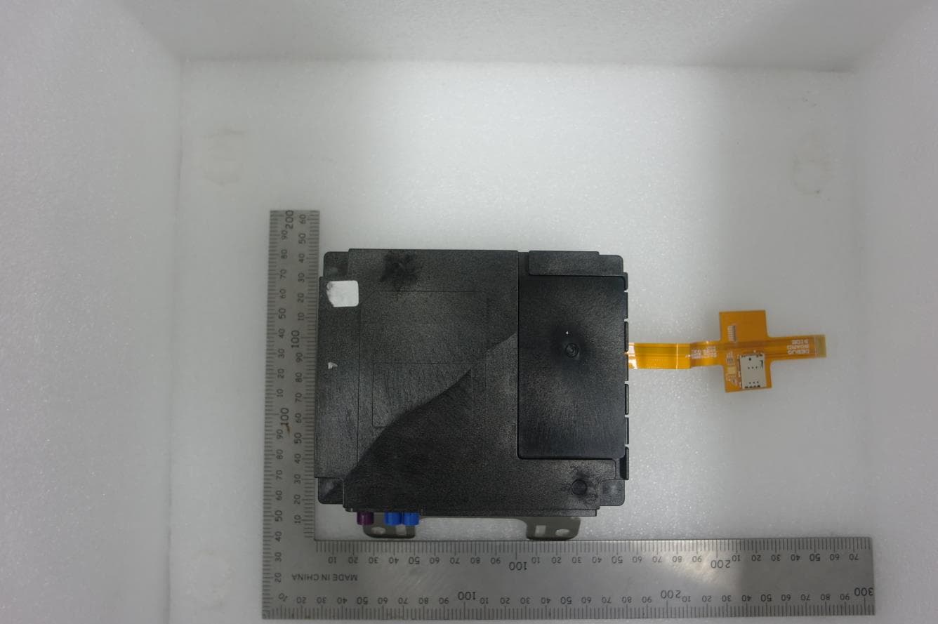
BEJTFHOBINI1F1
Jan 08, 2025Telematics
Equipment Class
DTS - Digital Transmission SystemBEJNT-16Z90TS
Oct 02, 2024Notebook Computer
Equipment Class
DSS - Part 15 Spread Spectrum TransmitterBEJSP-PEW8
Sep 26, 2024Stylus Pen
Equipment Class
DCD - Part 15 Low Power Transmitter Below 1705 kHzBEJ-RSMV2
Sep 24, 2024RF Module
Equipment Class
FDS - Part 15 Field Disturbance SensorBEJTFBMEIBN3EU
Sep 24, 2024Telematics
Equipment Class
NII - Unlicensed National Information Infrastructure TX