BEJ9QK-DMR3Wireless Adapter Card
LG Electronics USA, Inc.
Click to zoom
Application Details
- Equipment Class
- NII - Unlicensed National Information Infrastructure TX
- Date of Grant
- May 06, 2013
- Application Purpose
- Original Equipment
- Date of Application
- May 05, 2013
- Equipment Note
- Wireless Adapter Card
- Frequency Range
- 5180.00000000 - 5240.00000000
- Company
- LG Electronics USA, Inc.
- Country
- United States
Documents & Files
Document Text
Text extracted from the exhibit documents filed with the FCC. Open a document above to read the original.
Users Manual
Model Name : R3 Product Description. The Module is an OEM module (35x35mm) based on the SMSC DARR83. It is an uncompressed wireless digital audio transceiver operating in the 2.4GHz, 5.2GHz and 5.8GHz bands. The wireless audio link supports up to 4 stereo audio streams and comes together with additional features such as: data encryption, pairing functionality, bi-directional control data messages, low power audio snooze mode, WLAN detection and Automatic Frequency Allocation. The DARR83 chip itself provides the basic functions of Audio Processing and buffering, Data Link Layer and Physical Layer. The module integrates all functionality for a wireless digital audio connection, comprising: D ARR83 Wireless Audio Processor 2.4GHz/ 5. 2GHz/ 5.8 GHz RF Transceiver Embedded Antennas Digital audio interfaces (I 2 S and/or S/PDIF) I 2 C control interface 26 pins interface connector (FFC) for power, digital audio and control interface and GPIOs Built-in 1MB SPI interface Flash 3V 4KB uniform sector RF Frequency Bandwidth. 2.4GHz: 2400 – 2483.5MHz 5.2GHz: 5150 – 5250MHz 5.8GHz: 5725 – 5875MHz. RF Performance. For 2.4GHz application (VCC=3.3V, 25°C) Parameter Min Typ. Max Units RF Frequency Range 2400 2483.5 MHz Number of RF -Channels Carries in the spectrum 3 Transmission Power 14 dBm Frequency (dynamic or fixed allocation) Ch1 2412 MHz Ch2 2438 Ch3 2464 Channel Spacing 26 MHz RF Bandwidth Null-to-null 22 MHz Rx Sensitivity -83 dBm Antena Diversity Tx/Rx ON For 5.2GHz application (VCC=3.3V, 25°C) Parameter Min Typ. Max Units RF Frequency Range 5150 5250 MHz Number of RF -Channels Carries in the spectrum 3 Transmission Power Depending on antenna design 9 dBm Frequency (dynamic or fixed allocation) Ch1 5180 MHz Ch2 5210 Ch3 5240 Channel Spacing 30 MHz RF Bandwidth Null-to-null 22 MHz Rx Sensitivity -81 dBm Antena Diversity Tx/Rx ON For 5.8GHz application (VCC=3.3V, 25°C) Parameter Min Typ. Max Units RF Frequency Range 5725 5875 MHz Number of RF -Channels Carries in the spectrum 3 Transmission Power Depending on antenna design 9 dBm Frequency (dynamic or fixed allocation) Ch1 5736 MHz Ch2 5762 Ch3 5814 Channel Spacing 26 MHz RF Bandwidth Null-to-null 22 MHz Rx Sensitivity -81 dBm Antena Diversity Tx/Rx ON Air framing. Addressing : 24Bit. Data Message Size : 32Bytes CRC : 16, 24 and 32Bit POWER - Supply Voltage : 3.1V(Min), 3.3V(Typ), 3.5V(Max) - Peak to Peak Ripple : 100mV(Max). - Operating Temperature : -10C(Min), 25C(Typ), 60C(Max) Evaluation Board Usage The GUI is required to configure the evaluation boards for different applications. Step 1: Double-click on the GUI Icon or shortcut to run the program. Step 2: Read the limited license carefully. Click I Agree to proceed (as shown on the right). Step 3: Make sure the evaluation boards is turned on.. Step 4: Connect the USB cable between your notebook/PC and the evaluation board. If USB drivers are required to be installed, use the one provided in the GUI package. . Step 5: Setup your Com Port in Com Port Settings. Connect the USB one by one and select each unique USB port setting for each evaluation board. 1) Click the [Refresh] button. 2) Select the EVK ID, for example “A3UNG243”, to access the 4ch EVK connected to the DWAM83 module. 3) Click the [Apply] button. 4) (Optional) If the “A3UNG243”option cannot be selected from the drop down menu, click the [Disconnect] button before repeating steps 1 ~ 3. Once the connection is successful, you should see READY in Module Status. . If you see NOT FOUND, please check that the USB cable is properly connected/loose or 5V DC Power is plugged in. Step 6: At the top-left corner of the GUI, click Help and click About. The current firmware version is shown as Evaluation Kit Version X.X.X. The current GUI version is shown as Configuration Software GUI Version X.X.X. 2 1 3 4 Step 7: Setup your choice of application in the Application Selection (Power-up Settings) For the explanation for the different kinds of application, you can check the help file that is provided with the Evaluation board (EVK). Step 8: Click [Config] button (upon every change) to configure the evaluation board. Select desired application (depending on the number of Stereo sources required) Press this button whenever there are any changes in this section to update the module settings Select the Frequency band (2.4GHz or 5.2GHz or 5.8GHz) to operate after Configuration Select CU or MU mode 26Pin Interface PIN # PIN NAME IN/OUT DESCRIPTION 1 VDD Power Input Power: 3.3V. 2 GND Ground GND 3 MCLK In 24.56MHz Master Clock 4 BULE_LED I/O GPIO_13 5 RED_LED I/O GPIO_23 6 SDIO_W (FREQ_BAND) I/O GPIO_5 7 SDIO_X (DATA1) I/O GPIO_11 8 SDIO_Y (DATA2) I/O GPIO_6 9 SDIO_Z (UPLINK DATA) I/O GPIO_12 10 I2C_SCL_SLV I/O I2C SLAVE (SCL) 11 I2C_SDA_SLV I/O I2C SLAVE (SDA) 12 SPI_DI I/O SPI DATA IN 13 SPI_DO I/O SPI DATA OUT 14 SPI_CLK I/O SPI CLOCK 15 SPI_CS I/O SPI_MODE 16 SPI_WP I/O GPIO_1 17 RESET RESET 18 P_SENSE I/O GPIO_2 19 P_CTL I/O GPIO_7 20 PWM_RST I/O GPIO_4 21 AMP_PDN I/O GPIO_3 22 AMP_SD I/O GPIO_14 23 WIRELESS READY I/O GPIO_15 24 BCK (ROLE 1) I/O GPIO_8 25 GND Ground GND 26 LRCK (ROLE 0) I/O GPIO_10 Approval Statements Hereby, LG Electronics Inc. declares that this device is in compliance with the essential requirements and other relevant provisions of directive 1999/5/EC. This device complies with Part 15 of the FCC`s Rules. Operation is subject to the following two Conditions: 1. This device may not cause harmful interference, and 2. This device must accept any interference received, including interference that may cause undesirable operation. To satisfy FCC exterior labeling requirements, the following text must be placed on the exterior of the end product. Contains Transmitter module FCC ID: BEJ9QK-DMR3 This device complies with Industry Canada license-exempt RSS standard(s). Operation is subject to the following two conditions: (1) this device may not cause interference, and (2) this device must accept any interference, including interfer…
Text truncated - open the document above for the full version.
Cover Letter(s)
1. ANT A TEST 1) Layout and S - parameter 1) Layout and S parameter 1. ANT A TEST 2) Radiation Gain 2) Radiation Gain 2. ANT B TEST 1) Layout and S - parameter 1) Layout and S parameter 2. ANT B TEST 2) Radiation Gain 2) Radiation Gain
Cover Letter(s)
Request for Confidentiality Date: Apr. 24, 2013 Federal Communications Commission Authorization and Evaluation Division Subject: Confidentiality Request regarding Application for certification of FCC ID: BEJ9QK-DMR3 Gentlemen: Pursuant to Section 0.457 and 0.459 of the Commission’s Rules, we hereby request confidential treatment of information accompanying this application as outlined below: Functional Block Diagram Operational Description (theory of operation) Schematic Diagram The above materials contain trade secrets and proprietary information not customarily released to the public. The public disclosure of these materials may be harmful to the applicant and provide unjustified benefits to its competitors. The Applicant understands that pursuant to Section 0.457 of the Rules, disclosure of this application and all accompanying documentation will not be made before the date of the Grant for this application. Sincerely, _______________________________________ Jacob Cho Manager LG Electronics USA
Cover Letter(s)
Authority to Act as Agent Date: Aug. 15, 2012 American Certification Body, Inc. 6731 Whittier Avenue Suite C110 McLean, VA 22101 To Whom It May Concern: _____AUDIX Technology Corporation______ is authorized to act on our behalf, until otherwise notified, for applications to American Certification Body, Inc. (ACB). We certify that we are not subject to denial of federal benefits, that includes FCC benefits, pursuant to Section 5301 of the Anti-Drug Abuse Act of 1988, 21 U.S.C. 862. Further, no party, as defined in 47 CFR 1.2002 (b), to the application is subject to denial of federal benefits, that includes FCC benefits. Thank you, Agency Agreement Expiration Date: _____Aug. 15, 2013 _____ By: __________________________ __ Jacob Cho______ (Signature) (Print name) Title: _______Manager ______________ On behalf of: ___LG Electronics USA________ (Company Name) Telephone: _____1-201-266-2420 ___________
External Photos
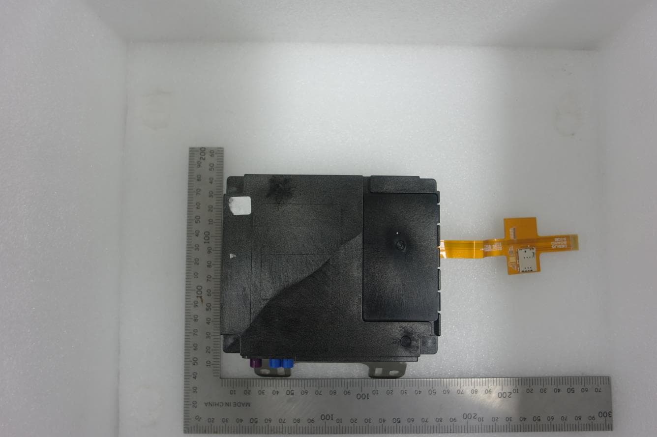
LG Electronics Inc. Wireless Adapter Card FCC ID. : BEJ9QK-DMR3 IC: 2703H-DMR3 EUT External Photos Figure 1 Wireless Adapter Card (Front View) Figure 2 Wireless Adapter Card (Back View)
ID Label/Location Info
LG Electronics Inc. Wireless Adapter Card FCC ID. : BEJ9QK-DMR3 IC: 2703H-DMR3 FCC ID & IC Label Location z Label Placement Location z FCC ID & IC Label Format FCC ID & IC Label Placement Location
Internal Photos
LG Electronics Inc. Wireless Adapter Card FCC ID. : BEJ9QK-DMR3 IC: 2703H-DMR3 EUT Internal Photos Figure 3 Wireless Adapter Card (Removed Shielded Case) Figure 4 Wireless Adapter Card (Front View)
RF Exposure Info
Declaration of Compliance FCC ID: BEJ9QK-DMR3 IC: 2703H-DMR3 Product Name: Wireless Adapter Card Model No: R3 LG Electronics Inc. declares that the product described above has been evaluated and found to comply with the RF exposure limits for humans, as specified based on ANSI/FCC recommendation. For WLAN(2.4GHz) Based on safety distance 20cm, the antenna gain is 1.0dBi, and the power output is 18.243mW, the power density is 0.0142mW/cm^. RF Exposure Calculations: S = (P * G) / (4* * r^2) or r = (P * G) / (4 * * S) Where S = Power Density in mW/cm^2 P=17.54dBm=56.754mw G =1.0dBi=1.259Numerical r = 20cm S = 56.754*1.259/ 4** 20^2 =0.0142mW/cm^ For WLAN(5.2GHz): Based on safety distance 20cm, the antenna gain is 3.0dBi, and the power output is 23.878mW,the power density is 0.0095mW/cm^2. RF Exposure Calculations: S = (P * G) / (4* * r^2) or r = (P * G) / (4 * * S) Where S = Power Density in mW/cm^2 P = 13.78dBm= 23.878mW G = 3.0dBi =1.995Numerical r = 20cm S = 23.878*1.995 / 4** 20^2 =0.0095mW/cm^2 For WLAN(5.8GHz): Based on safety distance 20cm, the antenna gain is 4.6dBi, and the power output is 35.584mW,the power density is 0.01869mW/cm^2 RF Exposure Calculations: S = (P * G) / (4* * r^2) or r = (P * G) / (4 * * S) Where S = Power Density in mW/cm^2 P = 15.13dBm =32.584mW G = 4.6dBi =2.884Numerical r = 20cm S = 32.584* 2.884/ 4** 20^2 =0.01869mW/cm^2 Sincerely Yours, ____________________________________ Mr. Ben Cheng Manager AUDIX Technology Corporation
Test Report
FCC ID: BEJ9QK-DMR3 IC: 2703H-DMR3 Page 1 of 40 AUDIX Technology Corporation Report No. EM-F1020318 APPLICATION FOR CERTIFICATION On Behalf of LG Electronics Inc. Wireless Adapter Card Model No.R3 FCC ID : BEJ9QK-DMR3 IC: 2703H-DMR3 Brand : LG Prepared for : LG Electronics Inc. 19-1, Cheongho-Ri, Jinwuy-Myeon, Pyeongtaek-City, Gyeonggi-Do, 451-713, Korea Prepared by : AUDIX Technology Corporation EMC Department No. 53-11, Dingfu, Linkou Dist., New Taipei City 244, Taiwan, R.O.C. Tel : (02) 2609-9301, 2609-2133 Fax: (02) 2609-9303 File Number C1M1304105 Report Number EM-F1020318 Date of Test Apr. 15 ~ 24, 2013 Date of Report Apr. 25, 2013 FCC ID: BEJ9QK-DMR3 IC: 2703H-DMR3 Page 2 of 40 AUDIX Technology Corporation Report No. EM-F1020318 TABLE OF CONTENTS Description Page TEST REPORT CERTIFICATION .......................................................................................................4 1. GENERAL INFORMATION .........................................................................................................5 1.1. Description of Device (EUT).................................................................................................................. 5 1.2. Tested Supporting System Details .......................................................................................................... 6 1.3. Description of Test Facility .................................................................................................................... 7 1.4. Measurement Uncertainty....................................................................................................................... 8 2. CONDUCTED EMISSION MEASUREMENT ............................................................................9 2.1. Test Equipment ....................................................................................................................................... 9 2.2. Block Diagram of Test Setup.................................................................................................................. 9 2.3. Powerline Conducted Emission Limit [§15.207, Class B, RSS-Gen §7.2.2/Table 2] ......................... 9 2.4. Operating Condition of EUT ................................................................................................................ 10 2.5. Test Procedure ...................................................................................................................................... 10 2.6. Powerline Conducted Emission Measurement Results......................................................................... 10 3. RADIATED EMISSION MEASUREMENT ..............................................................................13 3.1. Test Equipment ..................................................................................................................................... 13 3.2. Test Setup ............................................................................................................................................. 13 3.3. Radiated Emission Limits (§15.209, RSS-210 §2.7/Table 2)............................................................... 15 3.4. Operating Condition of EUT ................................................................................................................ 15 3.5. Test Procedure ...................................................................................................................................... 16 3.6. Test Results........................................................................................................................................... 17 4. 26dB BANDWIDTH MEASUREMENT .....................................................................................21 4.1. Test Equipment ..................................................................................................................................... 21 4.2. Block Diagram of Test Setup................................................................................................................ 21 4.3. Operating Condition of EUT ................................................................................................................ 21 4.4. Test Procedure ...................................................................................................................................... 21 4.5. Test Results........................................................................................................................................... 22 5. MAXIMUM PEAK OUTPUT POWER MEASUREMENT .....................................................25 5.1. Test Equipment ..................................................................................................................................... 25 5.2. Block Diagram of Test Setup................................................................................................................ 25 5.3. Specification Limits [§15.407(a)-(1), RSS-210 A9.2 (1)] .................................................................... 25 5.4. Operating Condition of EUT ................................................................................................................ 25 5.5. Test Procedure ...................................................................................................................................... 25 5.6. Test Results........................................................................................................................................... 26 6. POWER SPECTRAL DENSITY MEASUREMENT ................................................................27 6.1. Test Equipment ..................................................................................................................................... 27 6.2. Block Diagram of Test Setup................................................................................................................ 27 6.3. Specification Limits [§15.407(a)-(1), RSS-210 A9.2 (1)] ......…
Text truncated - open the document above for the full version.
Test Setup Photos
FCC ID: BEJ9QK-DMR3 IC: 2703H-DMR3 Page 37 of 40 AUDIX Technology Corporation Report No. EM-F1020318 10. PHOTOGRAPHS 10.1.Photos of Conducted Emission Measurement FRONT VIEW OF CONDUCTED MEASUREMENT BACK VIEW OF CONDUCTED MEASUREMENT FCC ID: BEJ9QK-DMR3 IC: 2703H-DMR3 Page 38 of 40 AUDIX Technology Corporation Report No. EM-F1020318 10.2.Photos of Radiated Measurement at Semi-Anechoic Chamber 10.2.1.Frequency Below 1GHz FRONT VIEW OF RADIATED MEASUREMENT BACK VIEW OF RADIATED MEASUREMENT FCC ID: BEJ9QK-DMR3 IC: 2703H-DMR3 Page 39 of 40 AUDIX Technology Corporation Report No. EM-F1020318 10.2.2. Frequency Above 1GHz FRONT VIEW OF RADIATED MEASUREMENT BACK VIEW OF RADIATED MEASUREMENT FCC ID: BEJ9QK-DMR3 IC: 2703H-DMR3 Page 40 of 40 AUDIX Technology Corporation Report No. EM-F1020318 10.3.Photo of Section RF Conducted Measurement 10.4.Photo of Maximum Peak Output Power Measurement
Contact Information
Applicant
David Kim(Team leader, LGEUS NA Policy & Regulatory Affairs)
Technical Contact
AUDIX Technology CorporationBen Cheng
[email protected]886 2609-9301
No. 53-11, Dingfu, Linkou Dist., · New Taipei City · Taiwan
Test Firm
Audix Technology CorporationJeff Chen
Technical Specifications
| # | Rule Parts | Frequency Range | Power Output |
|---|---|---|---|
| 1 | 15E | 5.18 GHz - 5.24 GHz | 23.88 mW |
Other Applications from LG Electronics USA, Inc.
BEJTFHOBINI1F1
Jan 08, 2025Telematics
Equipment Class
DTS - Digital Transmission SystemBEJNT-16Z90TS
Oct 02, 2024Notebook Computer
Equipment Class
DSS - Part 15 Spread Spectrum TransmitterBEJSP-PEW8
Sep 26, 2024Stylus Pen
Equipment Class
DCD - Part 15 Low Power Transmitter Below 1705 kHzBEJ-RSMV2
Sep 24, 2024RF Module
Equipment Class
FDS - Part 15 Field Disturbance SensorBEJTFBMEIBN3EU
Sep 24, 2024Telematics
Equipment Class
NII - Unlicensed National Information Infrastructure TX