BEJMU60PZ1060 Inch Plasma Display
LG Electronics USA, Inc.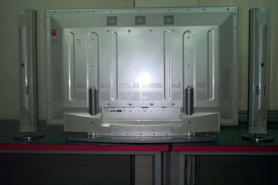
Click to zoom
Application Details
- Equipment Class
- JBP - Part 15 Class B Computing Device Peripheral
- Date of Grant
- Jul 19, 2001
- Application Purpose
- Original Equipment
- Date of Application
- Jul 19, 2001
- Equipment Note
- 60 Inch Plasma Display
- Company
- LG Electronics USA, Inc.
- Country
- United States
Documents & Files
Document Text
Text extracted from the exhibit documents filed with the FCC. Open a document above to read the original.
Users Manual
PLASMA DISPLAY PANEL ON/OFF INPUT SELECT VOLUME P/NO : 3828VA0277B(NP00KA) PLASMA DISPLAY PANEL Please read this owner’s manual carefully beforeoperating the Monitor.Retain it for future reference.Record model number and serial number of theMonitor.See the label attached on the back of the Monitorand quote this information to your dealer when yourequire service.Model number : DPDP60WSerial number : DPDP60W OWNER’S MANUAL ON/OFF INPUT SELECTVOLUME FCC NOTICE •DPDP60W : AClass B digital device This equipment has been tested and found to comply with the limits for a Class B digital device, pursuant to Part 15 of the FCC Rules. These limits are designed to provide reasonable protection against harmful interference in a residential installation. This equipment generates, uses and can radiate radio frequency energy and, if not installed and used in accordance with the instructions, may cause harmful interference to raido communications. However, there is no guarantee that interference will not occur in a particular installation. If this equipment does cause harmful interference to radio or television reception, which can be determined by turning the equipment off and on, the user is encouraged to try to correct the interfer- ence by one or more of the following measures: - Reorient or relocate the receiving antenna. - Increase the separation between the equipment and receiver. - Connect the equipment into an outlet on a circuit different from that to which the receiver is connected. - Consult the dealer or an experienced radio/TV technician for help. WARNING This is Class B product. In a domestic environment this product may cause radio interference in which case the user may be required to take adequate measures. WARNING TO REDUCE THE RISK OF FIRE AND ELECTRIC SHOCK, DO NOTEXPOSE THIS PROD- UCTTO RAIN OR MOISTURE. Keep this manual with Monitor for future easy refer- ence) Table of Contents First step WARNINGS..............................................................4 SAFETYINSTRUCTIONS........................................5 Composition Front Panel Controls................................................8 Connection Panel Overview.....................................9 Remote Control Key Functions/Accessories..........10 Installation of the monitor.......................................12 Connection VCR Setup..............................................................14 Cable TV Setup......................................................15 External AV Source Setup......................................16 DVD Setup..............................................................17 DTV Setup..............................................................18 PC Setup................................................................19 PC Computer Mode Feature Check.......................21 PC Computer Mode Adjustments...........................22 PIPfunction............................................................25 Twin picture function...............................................28 Using the remote control........................................30 Basic function Turning on the Monitor...........................................31 Selecting language for the menus..........................32 Checking features...................................................33 Time setting Setting sleep time...................................................34 Picture & Sound Auto picture control................................................35 Adjusting picture appearance.................................36 DRP(Digital Reality Picture)..................................37 Selecting screen item.............................................38 Adjusting sound appearance..................................39 Auto sound control.................................................40 AVL(Auto volume leveler)......................................41 Special function Using Still function..................................................42 Adjusting OSD Transparency.................................43 Setting picture format.............................................44 Others Maintenance...........................................................45 Troubleshooting check list......................................46 Product specifications.............................................47 4 WARNINGS WARNING: TO REDUCE THE RISK OF ELECTRIC SHOCK DO NOTREMOVE COVER (OR BACK). NO USER SERVICEABLE PARTS INSIDE. REFER TO QUALIFIED SERVICE PERSONNEL. The lightning flash with arrowhead symbol, within an equilateral triangle, is intended to alert the user to the presence of uninsulated “dangerous voltage” within the product’s enclosure that may be of sufficient magnitude to consti- tute a risk of electric shock to persons. The exclamation point within an equilateral triangle is intended to alert the user to the presence of important operating and maintenance (servicing) instructions in the literature accompanying the appliance. WARNING: TO PREVENTFIRE OR SHOCK HAZARDS, DO NOTEXPOSE THIS PRODUCTTO RAIN OR MOISTURE. CAUTION: TO PREVENTELECTRIC SHOCK, MATCH WIDE BLADE OF PLUG TO WIDE SLOT, FULLYINSERT. CAUTION: Do not attempt to modify this product in any way without written authorization from Zenith Electronics Corporation. Unauthorized modification could void the user’s authority to operate this product. The responsible party for this device compliance is: Zenith Electronics Corporation 201 James Record Road Huntsville, AL 35824, USA 1-877-993-6484 WARNING RISK OF ELECTRIC SHOCK DO NOT OPEN 5 First step Composition Connection Basic function T ime setting Picture & Sound Special function Others Important safeguards for you and your new product Your product has been manufactured and tested with your safety in mind. However, improper use can result in potential electrical shock or fire hazards. To avoid defeating the safeguards that have been built into your new product, please read and observe the following safety points when installing and using…
Text truncated - open the document above for the full version.
Block Diagram
FCC ID : BEJMU60PZ10 APPENDIX C : BLOCK DIAGRAM/SCHEMATATICS 1. PDP Module Block Diagram2. PDP Module Supplying Voltage & Current Diagram3. Power Board Block Diagram4. VSC Board Block Diagram5. Schematics 1. PDP Module Block Diagram FCC ID : BEJMU60PZ10 ... P 13 P 14 P 13 CON 100 CON207 V sc Vsc UP Vs ( 185V ) 15V 5V V sc ( 70V ) V setup( 260V ) 5V 5V 15V Va 입력 Buffer ( IC3 ) Energy Recovery IC 22 ( IPM1 ) Energy Recovery IC 23 ( IPM2 ) 5V 15V Vs 5V 5V 15V 입력 Buffer ( IC2 ) Protec -tor ( IC11 , 12 ) Protec -tor ( IC13 , 14 ) FET Driver ( IC 19 ) Photo Coupler ( IC 9 ) Buffer (IC15) FET Driver (IC17) Photo Coupler (IC 10) Buffer (IC16) FET Driver (IC18) Photo Coupler ( IC4 ∼ 7 ) 출력 Buffer ( IC20 ) SetDN SUS UP/DN Setup UP V setup Vsc DN Q17 Q11 ∼ Q16 Q19 Q1 ∼ Q10 Q18 SUS OUT A32 Y PCB 5V F 15V 5V F Clock , Data 5V Regulator ( IC 21) 15V 5V F 주입구 CON 2 Vs ( 185V ) 15V 5V 입력 Buffer ( U1 ) Energy Recovery ( IPM1 ) Energy Recovery ( IPM2 ) Protec -tor ( U2 , 3 ) Protec -tor ( U 5 ) FET Driver ( U 4 ) CON202CON206 CON203 RAMP Generator Vs 5V 15V Vs CON101 5V 5V 5V 15V A32 Z PCB Q1 SUSOUT X COF Y COF CON302 P 203 Shift Resister ( IC 17 ∼ 20 ) 입력 Buffer ( IC22 ) 입력 Buffer (IC301) CLK A/B , STB , BLK DATA FET 구동 ( IC302 ) ER 출력 ( Q 103,104 ) SUS 출력 ( IC303 ) P.C, FET 구동 (IC206,Q 101,2) A32 Rigid Left Top 5V 5V 5V 5V Va P 202 P 201 P 301 5V 15V Va 5V 5V 입력 Buffer (IC201) 입력 Buffer ( IC21 ) FET 구동 ( IC 202 ) ER 출력 ( Q 3,4 ) SUS 출력 ( IC 203 ) P.C, FET 구동 ( IC204,Q 1,2 ) CLK A/B , STB , BLK DATA Va 5V 5V 5V A32 Rigid Right Top CON 204 CON 208 CON 205CON 201 P 3 P 1 P 2 P 5 P 4 P 102 Y 출력 Buffer ( IC 510 ∼ 511 ) Timing 출력 Buffer ( IC 100 , 110 ) DATA 출력 Buffer ( IC101 ∼ 103 ) Timing 출력 Buffer ( IC 109 , 111 ) DATA 출력 Buffer ( IC 104 ∼ 108 ) Timing 출력 Buffer ( IC200 , 210 ) DATA 출력 Buffer ( IC 201 ∼ 203 ) Timing 출력 Buffer ( IC 209 , 211 ) DATA 출력 Buffer ( IC 204 ∼ 208 ) CON 100 Data Buffer ( IC501 ∼ 505 ) Sync Buffer ( IC506 ) Frame-MEM ( R,G,B ) ( IC 300 ∼ 302 ) RAM BANK1 ( IC 303 ∼ 304 ) RAM BANK2 ( IC 305 ∼ 306 ) EPROM ( IC 600 ∼ 601 ) Y TIMING OUT ( SUS & ER UP/DN , CLK ,DATA,STB ) Z TIMING OUT ( SUS & ER UP/DN ) Vs , Hs , BLK , DIS EN R,G,B Data Input ( 3*8 Bit) X TIMING OUT ( ER & SUS UP/DN , STB ,BLK ) X DATA OUT X DATA OUT A32 CONTROL PCB P 300 3.3V REG ( IC 10 ) 5 V 3.3 V SFM R,G,B Data SFM Data ( 1 ∼ 640 ) SFM Data ( 1 ∼ 640 ) Y COFY COFY COF 5 V 1 5 V 1 5 V 1 Clock Buffer (IC507) Clock Buffer (IC508) 5 V 1 To Data Buffer To Frame MEM Pix CLK SP-TC ASIC ( IC1 ) Z 출력 Buffer (IC 512) DA1 ASIC ( IC 2 ) IDA ODA 3.3 V 3.3 V 3.3 V3.3 V 3.3 V 40 ㎒ Crystal ( X1 ) Crystal Buffer (IC 401) SYSTEM Clock 3.3 V D 34 5 V 5 V X TIMING OUT ( ER & SUS UP/DN , STB ,BLK ) Signal Input ( R,G,B, H/V Sync ) 5 V 5 V 5 V 5 V X COF X COF X COF X COF P 4 P 5 Shift Resister ( IC 13 ∼ 16 ) P 3 P 2 P 1 Shift Resister ( IC 9 ∼ 12 ) Shift Resister ( IC 5 ∼ 8 ) Shift Resister ( IC 1 ∼ 4 ) 5V 15V Va CON304 Shift Resister ( IC 117 ∼ 120 ) 입력 Buffer (IC122) 입력 Buffer (IC401) CLK A/B , STB , BLK DATA FET 구동 ( IC 402 ) ER 출력 ( Q 107,108 ) SUS 출력 ( IC403 ) P.C, FET 구동 (IC207,Q105,6) A32 Rigid Left Bot 5V 5V 5V 5V Va Shift Resister ( IC 113 ∼ 116 ) X COF X COF P 104 P 105 P 206 P 6 CON301 5V 15V Va 5V 5V 입력 Buffer (IC501) 입력 Buffer (IC121) FET 구동 ( IC 502 ) ER 출력 ( Q 7, 8 ) SUS 출력 ( IC 503 ) P.C, FET 구동 ( IC 504,Q 5,6 ) CLK A/B , STB , BLK DATA Va 5V 5V 5V A32 Rigid Right Bot Shift Resister ( IC 109 ∼ 112 ) Shift Resister ( IC 105 ∼ 108 ) Shift Resister ( IC 101 ∼ 104 ) X COF X COF X COF CON 103 CON 102 CON 101 CON205 CON204 P 1 P 2 P 3 P 4 P 5 P 6 P 7 P 8 P 11P 12 2. PDP Module Supplying Voltage & Current Diagram FCC ID : BEJMU60PZ10 RIGID RIGHT TOP ... CON3 RIGID LEFT-TOP 주입구 RIGID LEFT BOT RIGID RIGHT BOT Y DRIVE CONTROLLER Z DRIVE voltage For V s DC Power Supply 185V 0.83A voltage For V a DC Power Supply 70V 0.49 A voltage For V set-up DC Power Supply 260V 0.024A voltage For V sc DC Power Supply 75V 0.02 A voltage For +5V(CTRL) DC Power Supply 5V 0.76A voltage For +5V DC Power Supply 5V 0.2 A voltage For +15V DC Power Supply 15V 0.28A < External DC Power Supply > < +5V , 0.017 A > < +15V , 0.028 A > < +Va , 0.098 A >< +5V , 0.113 A >< +15V , 0.12 A > < +Vs , 0.424 A > < +5V , 0.016 A > < +15V , 0.027 A > < +Va , 0.097 A > < +Vsc , 0.02 A > < +Vsetup , 0.024 A > < +5V , 0.761 A > < +5V , 0.024 A > < +15V , 0.028 A > < +Va , 0.133 A >< +5V , 0.002 A > < +15V , 0.048 A > < +Vs , 0.407 A > < +5V , 0.024 A > < +15V , 0.025 A > < +Va , 0.149 A > 0.126 Ap-p 0.168 Ap-p0.23 Ap-p 0.165 Ap-p 0.494 Ap-p 1.734 Ap-p 0.13 Ap-p 0.184 Ap-p 0.225 Ap-p 0.14 Ap-p 0.156 Ap-p 0.292 Ap-p 0.139 Ap-p 0.647 Ap-p 2.15 Ap-p 0.13 Ap-p 0.194 Ap-p 0.377 Ap-p 1.15 Ap-p 0.76 Ap-p 0.741 Ap-p Input Signal : Full WhiteCurrent ( Typ ) : mean 3. Power Board Block Diagram FCC ID : BEJMU60PZ10 EMI FILTER RECTIFIERRECTIFIER RUSH CONTROL POWER CONTROL PFC INDUCTOR Power Switching FET PFC 380V TINY 255P Auxillary Trans TINY 255P ST-BY Trans PFC Pack UC 3854 HIGH POWER FACTOR PREREGULATOR St-by 5V Aux. 16V STR- F6668B + MULTI TRANS Fly Wheel DIODE FLY BACK MODE Panel Ctl 5V Panel Drive 5V Sound 30V VSC 16V VSC 12V VSC 6V Step down Regulator SI-8120S Step down Regulator SI-8050S PANEL VIDEO SCAN CONVERTER Zero Current Resonant Mode Power FET 2sk2837 UC 3863 Resonant power supply mode IR 2113S High speed power FET driver UC 3863 Resonant power supply mode IR 2113S High speed power FET driver Power FET 2sk2837 VS 170-185 VA 72-80 SOUND FAN VSC ADRESS SUSTAIN DRIVE LOGIC P F C DC-DC ∼ VS Pack VA Pack EPROM CTL Pack 5V moni VS on VS on RL on Rush CTL 4. VSC Board Block Diagram FCC ID : BEJMU60PZ10 AC INPUT COMPONENT RGB-PC/ RGB-DTV AUDIO INPUT RGB INPUT/ CONTROL VPC3230D (Color decoder) 4H comb filter Y/C separator MSP3401 (Audio signa pocess, S/W) M52758FP (Video switch) switching signals input from two types of image and outputting them JAGASM (Scaler) Highly Integrated, Mixed Signal Flat Panel Display Processor SII150 (TMDS TX) 21P FLI2200 (Deinterlace) FLI2220 (Enhancer) …
Text truncated - open the document above for the full version.
External Photos
FCC ID : BEJMU60PZ10 1. External View [ Front ] [ Back ]
ID Label/Location Info
APPENDIX B : Labelling R equirements FCC ID : BEJMU60PZ10 Warning Label ID Label Warning Label Locati on ID Label Location
Internal Photos
FCC ID : BEJMU60PZ10 2. Internal View FCC ID : BEJMU60PZ10 3-1. Power Board FCC ID : BEJMU60PZ10 3-2. Control Board FCC ID : BEJMU60PZ10 3-3. VSC Board FCC ID : BEJMU60PZ10 3-4. X Board [ Left ] [ Middle ] FCC ID : BEJMU60PZ10 3-4. X Board [ Right ] FCC ID : BEJMU60PZ10 3-5. Y Board [ Whole ] FCC ID : BEJMU60PZ10 3-5. Y Board FCC ID : BEJMU60PZ10 3-6. Z Board [ Whole ]
Test Report
CONTENTS Page 1. GENERAL INFORMATION.....................................................................................................................4 1.1 D ESCRIPTIONS OF EQUIPMENT UNDER TEST (EUT)...................................................................................4 1.2 R EGULATIONS APPLIED TO EUT...............................................................................................................4 1.3 M EASUREMENT PROCEDURE.....................................................................................................................4 1.4 M EASUREMENT PLACE..............................................................................................................................4 2. GENERAL TEST CONDITIONS..............................................................................................................4 2.1 O PERATING CONDITIONS OF EUT.............................................................................................................4 2.2 S TABILIZATION OF EUT OPERATING.........................................................................................................5 2.3 T EMPERATURE AND HUMIDITY.................................................................................................................5 3. TEST SITE....................................................................................................................................................5 3.1 S EMI-ANECHOIC CHAMBER.......................................................................................................................5 3.2 A SHIELDED ENCLOSURE...........................................................................................................................5 4. CALIBRATIONS OF MEASURING INSTRUMENTS...........................................................................5 5. DESCRIPTION OF TEST CONDITION..................................................................................................5 5.1 P OWER LINE CONDUCTED EMISSION MEASUREMENTS...............................................................................5 5.2 R ADIATED EMISSIONS MEASUREMENTS.....................................................................................................6 6. MEASURING INSTRUMENTS AND SET-UP........................................................................................8 6.1 P OWER LINE CONDUCTED EMISSIONS........................................................................................................8 6.2 R ADIATED EMISSIONS...............................................................................................................................8 7. TEST DATA.................................................................................................................................................9 7-1. P OWER LINE CONDUCTED EMISSIONS (§15.107)......................................................................................9 7-2. R ADIATED EMISSIONS (§15.109)...........................................................................................................10 8. LIST OF INSTRUMENTS USED............................................................................................................11 9. SUPPORT DEVICE & ACCESSORIES USED......................................................................................12 9-1. S UPPORT DEVICE...................................................................................................................................12 APPENDIX A: TESTING GRAPH APPENDIX B: LABELING REQUIREMENT APPENDIX C: BLOCK DIAGRAM/SCHEMATIC APPENDIX D: TEST SETUP PHOTOGRAPHS APPENDIX E: EUT PHOTOGRAPHS APPENDIX F: USERS MANUAL APPENDIX G: SPECIFICATION 3/12 Report No. : 00431-4521-F1156 LG Electronics Inc. Q & R Center, 36, Munlae-dong, 6-ga, Youngdungpo-gu, Seoul, Korea Tel:+82-2-2630-3077~9, Fax:+82-2-2635-5543 1. GENERAL INFORMATION 1.1 Descriptions of equipment under test (EUT) 1.1.1 Manufacturer : LG Electronics Inc Kumi TV Plant 642 Jinpyoung-dong Kumi-City Kyoungsangbuk-do, 730-360, KOREA 1.1.2 EUT Type: 60 Inch Plasma Monitor 1.1.3 Model No. : MU-60PZ10B 1.1.4 Serial No. : Not attached 1.1.5 Trade Name : LG 1.1.6 FCC ID No. : BEJMU60PZ10 1.1.7 System characteristic and descriptions a) Max. Resolution: 1280 X 1024 (Dot) b) Port/Connector(s): Component Input(3X), A/V Input(3X), Speaker(2X), RGB-PC/RGB-DTV, Audio in(2X) c) Power Supply: AC 120V, ~60Hz, 320W 1.2 Regulations applied to EUT FCC Part 15 Class B : The Limit of CISPR 22 Class B apply in this test according to Part 15.107. e) and 15.109. g) 1.3 Measurement procedure ANSI C63.4-1992 1.4 Measurement place LG Electronics Inc. Quality and Reliability Center 36, Munlae-dong, 6-ga, Youngdungpo-gu, Seoul 150-096, Korea 2. GENERAL TEST CONDITIONS The test data contained in this report ware obtained by use of the measurement method recom- mended in FCC Rules, 47 C.F.R.§15.31(a)(6), with equipment and at the test site filed by the Federal Communications Commission(FCC). The technical standard for a computing device is setforth in the computing devices of Part 15 of FCC Rules. The measurement for radiated emis- sions and power-line conducted emissions were performed in accordance with the procedures described in ANSI C63.4-1992. 2.1 Operating conditions of EUT According to the requirements in the computing devices of Part 15, the measurement was made at each function of the EUT being connected with appropriate cables and peripherals. All measurement was investigated under operating conditions of clause 11.1 of ANSI C63.4- 1992. 4/12 Report No. : 00431-4521-F1156 LG Electronics Inc. Q & R Center, 36, Munlae-dong, 6-ga, Youngdungpo-gu, Seoul, Korea Tel:+82-2-2630-3077~9, Fax:+82-2-2635-5543 2.2 Stabilization of EUT operating The EUT was operated for sufficient minutes before testing to make it stabilized in a normal operating condition. The power supplied to the EUT was filtered to meet the requirements. 2.3 …
Text truncated - open the document above for the full version.
Test Report
FCC ID : BEJMU60PZ10 APPENDIX A : Test Graph 1. Radiated Emission 1-1. Audio/Video Input 1-2. Component/Audio Input 1-3. RGB-PC/Audio Input 2. Conducted Emissions 2-1. RGB PC/Audio Input, Component/Audio Input 2-2. Audio/Video Input FCC ID : BEJMU60PZ10 1-1 RADIATED EMISSIONS (A/V Input) FCC ID : BEJMU60PZ10 1-2 RADIATED EMISSIONS (Component/Audio Input) FCC ID : BEJMU60PZ10 1-3 RADIATED EMISSIONS (RGB-PC Input) FCC ID : BEJMU60PZ10 2-1 CONDUCTED EMISSIONS (RGB-PC,Component/Audio Input,) FCC ID : BEJMU60PZ10 2-2 CONDUCTED EMISSIONS (A/V Input,)
Test Report
APPENDIX G : Specification FCC ID : BEJMU60PZ10 154.3 (Pound)Weight10 57.3 X 34.8 X 3.9(Inch)Overall Dimension (W X H X D)9 1280 X 720Optimizing Resolution8 1280 X 1204Max. Resolution7 AC 120V ~ 60Hz, 320WRating6 BEJMU60PZ10FCC ID5 MU-60PZ10BModel Number4 LGTrade Name3 60 Inch Plasma MonitorEquipment Name2 FCC Part 15, Class BEquipment Class1
Test Setup Photos
FCC ID : BEJMU60PZ10 APPENDIX D : Test Setup Photographs 1. Radiated Emission 2. Conducted Emission FCC ID : BEJMU60PZ10 1. Radiated Emission FCC ID : BEJMU60PZ10 2. Conducted Emission
Contact Information
Applicant
David Kim(Team leader, LGEUS NA Policy & Regulatory Affairs)
Test Firm
LG Electronics Inc.K. Kim
Technical Specifications
| # | Rule Parts | Frequency Range | Power Output |
|---|---|---|---|
| 1 | 15B | - | - |
Other Applications from LG Electronics USA, Inc.
BEJTFHOBINI1F1
Jan 08, 2025Telematics
Equipment Class
DTS - Digital Transmission SystemBEJNT-16Z90TS
Oct 02, 2024Notebook Computer
Equipment Class
DSS - Part 15 Spread Spectrum TransmitterBEJSP-PEW8
Sep 26, 2024Stylus Pen
Equipment Class
DCD - Part 15 Low Power Transmitter Below 1705 kHzBEJ-RSMV2
Sep 24, 2024RF Module
Equipment Class
FDS - Part 15 Field Disturbance SensorBEJTFBMEIBN3EU
Sep 24, 2024Telematics
Equipment Class
NII - Unlicensed National Information Infrastructure TX