BRWXP6102JR XP6102 FM 6 channel radio system
Horizon Hobby, LLC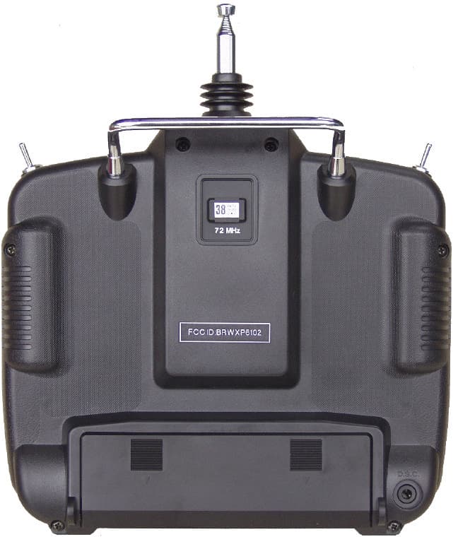
Click to zoom
Application Details
- Equipment Class
- TNB - Licensed Non-Broadcast Station Transmitter
- Date of Grant
- Dec 30, 2003
- Application Purpose
- Original Equipment
- Date of Application
- Sep 29, 2003
- Equipment Note
- JR XP6102 FM 6 channel radio system
- Frequency Range
- 72.01000000 - 72.99000000
- Company
- Horizon Hobby, LLC
- Country
- United States
Documents & Files
Document Text
Text extracted from the exhibit documents filed with the FCC. Open a document above to read the original.
Users Manual
INSTRUCTION MANUAL FOR AIRPLANE AND HELICOPTER FPO FPO FPO XP6102 6-CHANNEL COMPUTER RADIO SYSTEM CAN YOU FEEL IT? x SECTION 1 TABLE OF CONTENTS 2XP6102 - Introduction TABLE OF CONTENTS x 3XP6102 - Introduction x TABLE OF CONTENTS 4XP6102 - Introduction SECTION 1 x 5XP6102 - Introduction 1 USING THIS MANUAL In the beginning of this manual you will find the specifications for the radio and its various accessories. In addition, guidelines for the installation has been included. Instructions for setting all the functions and programs of the X-6102 are also included. These features are discussed in the same order that they will appear in your radio, as you will see on the accompanying pages. An explanation of the use and purpose of each feature is provided, followed by a labeled illustration of its respective LCD display. In addition, a step-by-step example clarifies the setup procedure of the feature. A blank data sheet has been included at the end of each section. Once all data has been input for a particular model, it is highly recommended that you record it on a copy of the sheet provided. If you should experience memory loss or battery failure or want to make changes to the current settings, this step will save you a great deal of time. CHAPTER 1: USING THIS MANUAL • INTRODUCTION 6XP6102 - Introduction 2.1 X-6102 TRANSMITTER The computer designed, ergonomically styled transmitter case ensures a comfortable fit in your hands. The ultra- precision control sticks offer adjustable spring tensions and length. The throttle stick offers a ratchet in Airplane configuration. 10-model memory storage allows programming of all parameters of ten separate helicopters or airplanes; you can program more than one setup for a single aircraft, allowing you to instantly change the flight characteristics. A five-year lithium backup battery prevents loss of memory in the event that the battery discharges completely or is removed. CHAPTER 2: FEATURES 2.2 R770 RECEIVER R770 (PCM Systems) The R770 is a high-performance PCM or single-conversion receiver with 10KHz super narrow band ABC&W circuitry. A narrow band ceramic filter for high- signal selectivity assists in rejecting cross modulations from other common radio frequencies-e.g. R/C transmitters, local paging systems. This receiver features Direct Servo Control (DSC) for control of surfaces without radio frequency output. The receiver has low current consumption. The R770's Slimline design allows it to fit into most model applications. S537 BALL BEARING SERVO 2.3 537 Servo • Wide spaced ball bearing for precise movement of your aircraft control outputs • A zero deadband amplifier insures accurate neutral centering • Low current drain • Indirect drive feedback potentiometer gives additional protection from vibration7 • 3-pole ferrite cored motor 7XP6102 - Introduction CHAPTER 3: COMPONENT SPECIFICATIONS SYSTEM SPECIFICATIONS 3.1 TYPE AIRPLANEHELICOPTER SYSTEM NAMEX-6102AX-6102H TRANSMITTER BODYNET-K236USNet-K236US RECEIVERR700 (FM) or R770 (PCM)R700 (FM) or R770 (PCM) CHARGERNEC-222NEC-222 AIRBORNE BATTERY1100mah1100mah SERVOSNES-537X4NES-537X5 ACCESSORIESStandard SwitchStandard Switch 12" Aileron Extension12" Aileron Extension Charge JackCharge Jack Servo AccysServo Accys Hex WrenchHex Wrench Instruction ManualInstruction Manual TRANSMITTER SPECIFICATIONS 3.2 TYPEAIRPLANEHELICOPTER MODEL NUMBERNET-K236USNET-K236US ENCODER6–channel computer system6–channel computer system RF MODULE72MHz72MHz MODULATIONPCM (s) or PPMPCM (s) or PPM OUTPUT POWERApproximately 750mwApproximately 750mw CURRENT DRAIN200mA (70mA with DSC)200mA (70mA with DSC) POWER SOURCE1.2Vx Ni-Cd (9.6V) 600mAh1.2Vx Ni-Cd (9.6V) 600mAh OUTPUT PULSE1000–2000 (1500 Neutral)1000–2000 (1500 Neutral) 3.3 SERVO SPECIFICATIONS TYPE537 TORQUE (ounce inch)43 oz/in SPEED (sec/60°).25 60° WEIGHT1.58 SIZE (in) (L x W x H)1.52 x 0.73 x 1.32 BBSingle MOTOR3-Pole Ferrite 8XP6102 - Introduction 3.4 RECEIVER SPECIFICATIONS TYPEFMPCM MODEL NUMBERR700R770 TYPE7 Channel / FM-ABC&W / Micro7 Channel / FM-ABC&W / Micro FREQUENCY72MHz72MHz SENSITIVITY (Microseconds)5 uS minimum5 uS minimum SELECTIVELY8KHz / 5 dB8KHz / 5 dB WEIGHT (oz)1.51.5 RECEIVER ANTENNA39“ for all aircraft frequencies39“ for all aircraft frequencies 3.5 CHARGER SPECIFICATIONS TYPEAIRCRAFTHELICOPTER MODEL NUMBERNEC-222NEC-222 INPUT VOLTAGEAC 100–120VAC 100–120V OUTPUT CURRENT50mAh TX/120mAh RX50mAh TX/120mAh RX CHARGING TIME15 Hours15 Hours 3.6 AIRBORNE BATTERY PACK TYPEAIRCRAFTHELICOPTER MODEL NUMBERB1100B1100 VOLTAGE4.8 V4.8 V SIZE (in) (W x L x H)2.24 x 0.63 x 1.702.24 x 0.63 x 1.70 WEIGHT (oz)4.94.9 CHAPTER 4: BATTERY CHARGING TRANSMITTER/RECEIVER 4.1 Note: It is imperative that you fully charge both the transmitter and the receiver battery packs prior to each trip to the field. To do so, leave the charger and batteries hooked up overnight (16 hours). The first charge should be approximately 20–24 hours in order to fully charge both battery packs to peak capacity. The charger supplied with this system is designed to recharge your batteries at a rate of 50mAh for the transmitter and 120mAh for the receiver battery pack. Transmitter Only The center pin on all JR Remote Control Systems is negative. Therefore, the center pin on all JR chargers is negative, not positive. This is different from many other manufacturers' chargers and radio systems. Beware of improper connections based on "color-coded" wire leads, as they do not apply in this instance. You must make sure that the center pin of your JR transmitter is always connected to the negative voltage for correct polarity hookup. Important: Please note that the charging polarity of the transmitter and receiver are different. 9XP6102 - Introduction CENTER PIN IS NEGATIVE OUTSIDE IS POSITIVE RIGHT SIDE OF TRANSMITTER RED–POSITIVE / BROWN–NEGATIVE / ORANGE–SIGNAL RED TO NEGATIVE BLACK TO POSITIVE CHARGER PIGTAIL FOR TRANSMITTER CHARGER PIGTAIL FOR RECEIVER CHARGER 4.2 The pilot lamps should always be on…
Text truncated - open the document above for the full version.
Block Diagram
Page 6 Technical Report Transmitter Model XP6102 FCC ID# BRWXP6102 3.2 Block Diagram (Reference is made to Figure 5.1) The (up to) four control potentiometers are at the left side of the schematic drawing. The control potentiometer, which is mechanically coupled to the control (joy) stick, is supplied with the regulated 5.0V voltage. The wiper on this pot is exactly centered in the neutral control stick position. All analog processing is performed as deviations from this center (reference) voltage. After the mixing of each channel, control voltage is changed to Pulse Train, through encoder circuit. The oscillator consists of an ECO type oscillator, excited by a quartz crystal. The crystal supports oscillation at the crystal's fundamental frequency (approximately 18MHz). The tuned circuit in the oscillator transistor's collector is tuned to the second harmonic of this frequency (approx. 36MHz). Q12 acts as a frequency multiplier (×2)/buffer; it drives the Power Amplifier (PA). Its output frequency is 4× crystal frequency. The straight-through PA stage is followed by a matching and band pass/low-pass network. This network matches the low PA stage output impedance to the whip antenna. The crystal load capacitance is affected by varicap D11, which is voltage-controlled by the "rounded-off square wave from the modulator transistor. The oscillator frequency is therefore switched in the rhythm of the modulate modulation pattern (FSK). Two DC Supply Voltage enter the RF section: 9.6 Volt "law" battery voltage supplies the PA stage only. All other stages, and bias current for all stages, including the PA, are derived from the regulated 6.0 Volt source on the RF board.
Block Diagram
FMTRANSMITTERBLOCKDIAGRAMXP610272MHz Xtal18MHz72MHzANT OSCDoblerAmp.PowerAmp.BandPass Q11Q12Q13Filter 2SC28592SC46932SC4910 Modulator Q14,Q15Regulator 2SC2712Q16;2SC3265 RF;72MHzFMD11;1SV231D13;02DZ6.8Y LCD LCD32-52 DSC/TRN. CPU1 Channel1~4M38C89MF StickTrim Clock6.8269MHzBZ FunctionSWSystem 10PCS.Control Editkey9.6VBKUP SW15-SW203V ENCODER FCCID#BRWXP6102Figure5.1TransmitterBlockDiagram
Cover Letter(s)
September 25, 2003 Federal Communications Commission Equipment Authorization Division, Applications Processing Branch 7435 Oakland Mills Road Columbia, MD 21046 RE) FCC ID: BRWXP6102 To whom it may concern; Please refer to the additional information listed below while reviewing the BRWXP6102 System. 1) Section 95.645 (b) states that plug-in crystals must not be accessible to the user. Indicate whether or not crystals are accessible to the user. Although the transmitter crystal is visible from the back of the transmitter, each crystal is glued in place prior to shipment making it a permanent installation. Consumer removal of the crystal will normally result in damage to the crystal. Therefore, frequency changes are done at the service center only. 2) The Manual must contain warnings per section 95.653 A) Please refer to the manual attachment for this information B) All content for operation is contained in the instruction manual. 1) All instructions are contained in the instruction manual. 2) There are no adjustments accessible to the user that would be in violation with the FCC rules. 3) This section is not applicable to our use. If there is any further information required, please contact me directly at: Horizon Hobby Distributors ATTN: Peter Bergstrom Fax: 217-355-0058 Phone: 217-403-3202 [email protected]
Cover Letter(s)
READ INSTRUCTIONS CAREFULLY Approved by OMB BEFORE PROCEEDING FEDERAL COMMUNICATIONS COMMISSION 3060-0589 REMITTANCE ADVICE Page No__ of__ SPECIAL USE ONLY (1) LOCKBOX # FCC USE ONLY SECTION A – PAYER INFORMATION (2) PAYER NAME (if paying by credit card enter name exactly as it appears on the card) (3) TOTAL AMOUNT PAID (U.S. Dollars and cents) (4) STREET ADDRESS LINE NO.1 (5) STREET ADDRESS LINE NO. 2 (6) CITY (7) STATE (8) ZIP CODE (9) DAYTIME TELEPHONE NUMBER (include area code) (10) COUNTRY CODE (if not in U.S.A.) FCC REGISTRATION NUMBER (FRN) REQUIRED (11) PAYER (FRN) (12) FCC USE ONLY IF MORE THAN ONE APPLICANT, USE CONTINUATION SHEETS (FORM 159-C) COMPLETE SECTION BELOW FOR EACH SERVICE, IF MORE BOXES ARE NEEDED, USE CONTINUATION SHEET (13) APPLICANT NAME (14) STREET ADDRESS LINE NO.1 (15) STREET ADDRESS LINE NO. 2 (16) CITY (17) STATE (18) ZIP CODE (19) DAYTIME TELEPHONE NUMBER (include area code) (20) COUNTRY CODE (if not in U.S.A.) FCC REGISTRATION NUMBER (FRN) REQUIRED (21) APPLICANT (FRN) (22) FCC USE ONLY COMPLETE SECTION C FOR EACH SERVICE, IF MORE BOXES ARE NEEDED, USE CONTINUATION SHEET (23A) CALL SIGN/OTHER ID (24A) PAYMENT TYPE CODE (25A) QUANTITY (26A) FEE DUE FOR (PTC) (27A) TOTAL FEE FCC USE ONLY (28A) FCC CODE I (29A) FCC CODE 2 (23B) CALL SIGN/OTHER ID (24B) PAYMENT TYPE CODE (25B) QUANTITY (26B) FEE DUE FOR (PTC) (27B) TOTAL FEE FCC USE ONLY (28B)FCC CODE I (29B) FCC CODE 2 SECTION D – CERTIFICATION CERTIFICATION STATEMENT I, , certify under penalty of perjury that the foregoing and supporting information is true and correct to the best of my knowledge, information and belief. SIGNATURE_______________________________________________________________ DATE _________________________ SECTION E - CREDIT CARD PAYMENT INFORMATION MASTERCARD______ VISA_______ AMEX_______ DISCOVER_______ ACCOUNT NUMBER_____________________________________________________ EXPIRATION DATE ____________________________________ I hereby authorize the FCC to charge my credit card for the service(s)/authorization herein described. SIGNATURE__________________________________________________________________________ DATE_____________________________________ SEE PUBLIC BURDEN ON REVERSE FCC FORM 159 FEBRUARY 2003(REVISED) ADVICE REFERENCE GUIDE HOW TO USE FCC FORM 159-REMITTANCE ADVICE The FCC Form 159, "Remittance Advice,” and FCC Form 159-C, (Continuation Sheet) is a multi-purpose form that must accompany any payment to the Federal Communications Commission (e.g., Regulatory Fees, Processing Fees, Auctions, Fines, Forfeitures, Freedom of Information Act (FOIA) Billings, or any other debt due to the FCC). The information on this form is collected to ensure credit for full payment, to ensure you receive any refunds due, to service public inquiries, and to comply with the Debt Collection Improvement Act of 1996. Note: Fee Filing Guides can be obtained by calling Forms Distribution -- (202) 418-3676 or 1-800-418-3676, or by calling FCC's fax-on-demand -- (202) 418-0177 from the handset of a fax machine. Instructions for Completing FCC Form 159 & 159-C NOTE: All required blocks must be completed or it may result in a delay in processing or the return of your application. (1) Lockbox No. # - Enter the appropriate six-digit P.O. Box Number as found in either the FCC Fee Filing Guide for the service requested, or as specified in the Public Notice. SECTION A (2) Payer Name - Enter the name of the person or company (i.e., maker of the check) making the payment. If using an individual name, enter the last name, first name, and middle initial. If a company, enter the name used commercially. If paying by credit card, enter the name exactly as it appears on your card. (3) Total Amount Paid - Enter the total amount of your remittance. (4) Street Address Line 1 - The street address or post office box number to which correspondence should be sent. (5) Street Address Line 2 - This line may be used if further identification of the address is required. (6) City - The name of the city associated with the street address given in (4). (7) State - If the payer has a United States mailing address enter the appropriate two-digit state abbreviation as prescribed by the U.S. Post Office. If the payer has a mailing address outside the United States, leave this section blank. (8) ZIP Code - Enter the appropriate five or nine-digit ZIP code prescribed by the U.S. Post Office. If address is foreign, enter the appropriate ZIP (postal) code. (9) Daytime Telephone Number - Enter the payer's ten-digit daytime telephone number, including area code. For foreign telephone numbers include the appropriate country dialing access code, as if you were calling from the United States. This daytime number should be the number where you can be reached during normal business hours. (10) Country Code - This section is for payers who have an address outside the United States of America. Enter the appropriate code here. To obtain country code information, contact the Mailing Requirements Dept. of the U.S. Postal Service. (11) Payer (FRN) - Enter the payer's ten-digit FCC Registration Number (FRN) assigned by the Commission Registration System (CORES). The FRN is a unique entity identifier for everyone doing business with the Commission. The FRN can be obtained electronically through the FCC webpage (www.fcc.gov.com) or by requesting FCC Form 160 through the FCC forms webpage (www.fcc.gov/formpage.html). (12) FCC Use Only (You must complete Section A - Block 11: FCC Registration Number) SECTION B COMPLETE THIS SECTION IF THE PAYER AND APPLICANT ARE DIFFERENT (13) Applicant Name - Enter the name (last, first, middle initial) as it appears on the original application or filing being submitted. Applicant includes Licensees, Regulatees or Debtors. If you are using this form to pay for multiple applicants with a single remittance, each applicant must be listed separately using the continuation sheet - Form 159-C. (If the name is the same as the payer (bloc…
Text truncated - open the document above for the full version.
Operational Description
Page 4 Technical Report Transmitter Model XP6102 FCC ID# BRWXP6102 2.0 ENCODER THEORY OF OPERATION Reference is made to Figure 5.1, Transmitter Block Diagram. The functions of the encoder are to: * accept the analog voltages from the control inputs (joysticks, toggle switch). * process the analog voltages to create control mixing, adding, reversing, etc., as desired by the user. * sample these voltages in a cyclic rhythm under control of the system's internal timing generator. (This process is called commutation.) * process these analog voltages into binary weighted digital control words by means of an Analog-to-Digital Converter (ADC). * store these digital representations of the analog control input into a temporary memory (RAM). * supply this serial data stream to a buffer-driver for modulation of the RF Transmitter. * provide "housekeeping" of the encoding process by means of a quarts crystal controlled internal clock. * provide supply voltages to the RF section (Vcc = 9.6V battery voltage; Vreg = 6.0V regulated voltage). The entire program which controls the timing housekeeping, parallel-to-serial conversion process, and insertion of synchronization words and error detection codes is governed by a Central Processing Unit (CPU) under control by an internally stored program residing in Read-Only Memory (ROM). The CPU, RAM and ROM are all part of a single-chip microprocessor. Resolution of the Analog-to-Digital conversion process is ten (10) bits for a control accuracy of 1:2 10
Operational Description
Page 5 Technical Report Transmitter Model XP6102 FCC ID# BRWXP6102 3.0 THEORY OF OPERATION 3.1 General Reference is made to Figure 5.1, Transmitter Block Diagram. The HORIZON HOBBY DISTRIBUTORS, INC. Model XP6102 R/C Transmitter is sticks type Transmitter. It operates on any of the R/C frequency (Channels) allowed by the Commission in the 72 -73 MHz frequency band. Selection of the desired RF channel is made by Quarts crystal. This transmitter employs Frequency-Sift-Keying (FSK) of the carrier frequency, whereby the output frequency is either low or high due to the symmetrical FSK modulation process, the (center) output frequency cannot be directly measured, but must be calculated by taking the average of the high and low frequency states. m m m = shift from center frequency m = approx.1.8KHz F low fc f high f carrier = (f low +f high )/2 The peak-to-peak deviation of the FSK signal is approximately 3.6 KHz ("sliver modulation") Because of the unfamiliarity of the general public with the term FSK, this modulation technique is commonly named FM.
Parts List/Tune Up Info
Technical Report Transmitter Model XP6102 FCC ID# BRWXP6102 5.4 Transmitter R.F. Tune-Up Procedure 1. Remove 6 screws from transmitter. Break seal on case and remove PC assembly. Put PC assembly on bench, component side up. 2. Refer to transmitter schematic Figure 5.2.2. Soften bee’s wax on cores in L11, L12, L13 and L14. Using oscilloscope with small 50 ohm loop, starting at L11, adjust these cores for maximum oscilloscope reading. Repeat this tuning sequence until no further increase in oscilloscope reading can be obtained. 3. The MOD. IN input latch at 0 volt. Observe frequency counter. Adjust the small ceramic trimmer capacitor on the PC assembly so that output frequency is exactly 1.8 KHz higher than the channel frequency. 4. The MOD. IN input latch at 9.6 Volt. Adjust the small trimmer resistor on PC assembly so that output frequency is exactly 1.8 KHz lower than channel frequency for the module. 5. Repeat step 2. Repeat step 3 and 4. 6. Using spectrum analyzer with small 50 ohm loop, verify that sub harmonic and harmonic components are at least 50dB below carrier component. Pay special attention to 90MHz and 144 MHz components. 7. Remove PC assembly from Transmitter. Reapply bee’s wax to L11, L12, L13 and L14. Put PC assembly back into its case, replace the four screws and re-seal opposite edge.
Schematics
FMTRANSMITTERBLOCKDIAGRAMXP610272MHz Xtal18MHz72MHzANT OSCDoblerAmp.PowerAmp.BandPass Q11Q12Q13Filter 2SC28592SC46932SC4910 Modulator Q14,Q15Regulator 2SC2712Q16;2SC3265 RF;72MHzFMD11;1SV231D13;02DZ6.8Y LCD LCD32-52 DSC/TRN. CPU1 Channel1~4M38C89MF StickTrim Clock6.8269MHzBZ FunctionSWSystem 10PCS.Control Editkey9.6VBKUP SW15-SW203V ENCODER FCCID#BRWXP6102Figure5.1TransmitterBlockDiagram
Schematics
A A B B C C D D E E F F G G H H I I J J K K 11 22 33 44 55 66 77 88 RF PCB 3 2 1 7 6 5 4 1 2 3 7 6 5 4 1 2 3 7 6 5 4 1 2 3 7 6 5 4 1 23 7 12 3 4 56 7 12 3 4 56 1 23 456 1 23 456 1 23 456 1 2 3 4 56 ST2 ST1 3 2 1 1 2 3 456 ST4 ST3 RES 1 2 34 56 7 1 23 456 7 1 23 4 5 6 1 2 3 4 56 1 23 456 103 C10 R30 1K R31 1K R32 1K1K R33 R13 1K R14 1K R15 1K1K R16R17 1K R18 1K R19 1K1K R20R21 1K R22 1K R23 1K1K R24 103 C11 R25 1K1K R26 R27 1K1K R28 6.8269 10p C15 10p C16 103 C19 105 C18 2.2K R11 1K R12 1K R29 1K R34 1K R36 1K R38 1K R40 1K R46 C23 103 R55 12K 103 C24 C29 102 123 456 C12 103 105 C26 474 C27 105 C28 105 C30 474 C32 474 C34 474 C33 R8 22K R10 10K C17 102 R48 1.6K D5 1SR35 VR3 Stick VR4 Stick 102 C22 103 C13 1K R44 22K R42 CN4BCN1BCN2B CN5CN6 CN6B CN8 C9 102 R2 2.2K Q3 2SC2712 CN12 R57 470K 22K R56 Q6 2SC2712 Q5 2SA1037 C4 103 Q2 2SC2712 Q1 2SC3265 D3 1SS352 D1 1SS352 R1 2.7K R3 100K Litum 3v D2 1SS352 C1 104 C2 103 C3 16V/10uF C6 16V/10uF C5 104 C7 10V/100uF 10K R4 Q4 2SC2712 R59 22K VR1 Stick VR2 Stick R61 1K NC Vcc Sub Out Gnd 213 54 PST9140 U2 R6 4.7K R5 7.5K C8 103 U1 78L05F 1K R43 103 C21 103 C14 102 C20 1 2 SW1 1 2 SW9 CN4 CN3 103 C47 103 C46 103 C45 103 C44 CN2CN1 103 C51 103 C50 103 C49 103 C48 1 2 SW2 1 2 SW10 CN3B 1 2 SW3 1 2 SW11 1 2 SW4 1 2 SW12 103 C43 103 C42 103 C41 103 C40 1 2 SW8 + FLP 1 2 SW14 - 12 Tsw6 CUT Tsw3 D/R Tsw4 HOLD 12 SW16 Down 12 SW15 Up 12 SW18 Inc 12 SW17 Dec 12 SW20 Clear C39 103 C36 103 C37 103 C38 103 36 35 34 33 32 30 29 28 27 26 25 24 23 22 21 20 31 19 18 17 16 15 14 13 12 11 10 9 8 7 6 5 4 3 2 1 73 74 75 76 77 78 79 80 81 82 83 84 85 86 87 88 89 90 91 92 93 94 95 96 97 98 99 100 101 102 103 104 105 106 107 108 373839404142434445464748495051525354555657585960616263646566676869707172 109110111112113114115116117118119120121122123124125126127128129130131132133134135136137138139140141142143144 SEG32SEG33SEG31SEG30SEG29SEG28SEG26SEG25SEG24SEG23SEG22SEG21SEG20SEG27SEG19SEG18SEG17SEG16SEG15SEG14SEG13SEG12SEG11SEG10SEG9SEG8COM23COM22C0M21COM20COM19COM18COM17COM16COM7COM6 COM8COM9 COM10COM11COM12COM13 AN0AN1AN2AN3 NCNC XINVSS OSCSEL XOUT VCC NC XCIN XCOUT NC RESET AN4P11P12P13P14P15P16P17P00P01P02P03P04P05 P06 P07 INT0 P41 BEEP+ CNTR1 RXD/P44 P46 P20 P21 P22 P23 P24 P25 P26 P27 TXD P47 VSS NC NC VLIN C1 C2 C3 VL5 VL4 VL3 VL2 VL1 COM0 C0M1 COM2 COM3 COM4 COM5 COM14 COM15 COM24 COM25 COM26 COM27 COM28 COM29 COM30 COM31 SEG59 SEG58 SEG57 SEG56 SEG55 SEG54 SEG53 SEG52 SEG51 SEG50 SEG49 SEG48 SEG47 SEG46 SEG45 SEG44 SEG43 SEG42 SEG41 SEG40 SEG39 SEG38 SEG37 SEG36 SEG35 SEG34 CPU M38C89MF CPU1 12 SW19 Channel 27K R47 13K R50 6.8K R51 3.3K R52 2.2K R53 105 C25 2468 1012141618202224262830323436384042 444648505254565860626466687072747678808284 LCD32-52 1K R45 R62 1K CN7CN7B RED BLACK 1 2 3 4 5 6 33K R54 CN10B ORENGE GRAY CN6 CN9B FUSE 3A D4 1SR35 CN10 1 2 3 R7 22K CN5B 1 2 + AUX SW7 1 2 _ SW13 12 TRN SW5 Tsw2 D/R Tsw1 Ge VSS VDD CLR D CK PR QQ CLR D CKPRQQ 74HC74 1234567 89 1011121314 U3 R58 820 C35 102 C31 16V/10uF R60 1.8K 1K R49 CN8B
Schematics
A A B B C C D D E E F F G G H H I I J J 11 22 33 44 55 66 77 Vcc 6V 53LSS L4 L7 3.3uH 2SC2859Y Q11 560 R74 X1 72MHz D11 1SV231 10K R73 10KR72 10KR71 33 R75R7612K R77 3.3K 2SC4693 Q12 10 R78 10 R79 220 R80 24 R82 3.3K R81 2SC4910 Q13 10 C84 10 R83 470R85 ( 8t ) F72C L5 CH18P C88 CH100P C89 CH47P C91 102 C85 103 R84 C81 CH10P C80 CH12P C82 B470P C79 CH3P ANT C72 CH220P C70 CH220P C74 103 C76 CH47P C75 CH68P C78 103 C77103 2.2K R86 1KP1 680 R87 470 R88 2SC2712GR Q14 JPW R89 film 182J C107 10K R90 4.7K R92 30K R91 2SC2712GR Q15 102 C96 10K R93 02DZ6.8Y D12 2SC3265Y Q16 103 C98 103 C97 680 R94 103 C99 C83 103 L6 F72C ( 8t ) 103 C93 103 C108 103 C101 C103 103 R70 10 103 C100 GND. MOD. Vcc JPW C90 VC1 20PF C86 CH8P C102 103 CH8P C71 L3 TW72S L2 TW72S L1 TW72S CH1P C104 CH82P C111 CH2PC110
Test Report
A-007-03-C Page 1 of 20 KEC Ikoma Testing Laboratory 12128 Takayama-cho Ikoma-city Nara 630-0101 Japan KANSAI ELECTRONIC INDUSTRY DEVELOPMENT CENTER HEAD OFFICE IKOMA TESTING LABORATORY 6-8-7 NISHITENMA 12128 TAKAYAMA-CHO KITA-KU OSAKA 530-0047 JAPAN IKOMA-CITY NARA 630-0101 JAPAN Corporate Juridical Person TEST REPORT Report No.A-007-03-C Date: 29 August 2003 This test report is to certify that the tested device properly complies with the requirements of: FCC Rules and Regulations Part 95 : Radio Control (R/C) Radio Service. The tests necessary to show compliance to the requirements were performed and these results met the specifications of requirement. The results of this report should not be construed to imply compliance of equipment other than that, which was tested. Unless the laboratory permission, this report should not be copied in part. 1. Applicant Company Name : JAPAN REMOTE CONTROL CO., LTD. Mailing Address : 2-2-12, EIWA, HIGASHIOSAKA-CITY, OSAKA, 577-0809 JAPAN 2. Identification of Tested Device Type of Device : Radio Control (R/C) Transmitter Kind of Equipment Authorization : : DoC : Certification : Verification FCC ID : BRWXP6102 Device Name : FM 6-CHANNEL TRANSMITTER Trade Name : JR PROPO Model Number : XP6102 Serial Number : No.1 : Prototype : Pre-production : Production Date of Manufacture : July 2003 3. Test Items and Procedure : RF Power Output (Substitution Method) : Modulation Characteristics : Emission Bandwidth : Field Strength of Spurious Radiation : Frequency Stability Measurement Above all tests were performed under: FCC Part 2 Sec2.1046, Sec2..1047, Sec2.1049, Sec2.1053, Sec2.1055 and Sec2.1057. : without deviation, : with deviation (details are found inside of this report) 4. Date of Test Receipt of Test Sample : 1 August 2003 Condition of Test Sample : : Damage is not found on the set. : Damage is found on the set. (Details are described in this report) Test Completed on : 25 August 2003 Seiichi Izumi General Manager of Ikoma Testing Laboratory A-007-03-C Page 2 of 20 KEC Ikoma Testing Laboratory 12128 Takayama-cho Ikoma-city Nara 630-0101 Japan Table of Contents 1. GENERAL INFORMATION ................................................................................................ 3 1.1. Product Description .....................................................................................................3 1.2. Description for Equipment Authorization .................................................................3 1.3. Test Facility ..................................................................................................................3 2. TESTED SYSTEM ............................................................................................................... 4 2.1. Test Mode ......................................................................................................................4 2.2. Block Diagram of EUT System ...................................................................................4 2.3. List of EUT System......................................................................................................5 2.4. List of Antenna .............................................................................................................5 3. RF OUTPUT POWER AND RADIATED SPURIOUS EMISSIONS .................................. 6 3.1. Reference Rule and Specification ...............................................................................6 3.2. Test Procedure ..............................................................................................................6 3.3. Test Configuration .......................................................................................................7 3.4. Photographs of EUT System Configuration ..............................................................9 3.5. Test Results ................................................................................................................10 4. MODULATION CHARACTERISTICS...............................................................................11 4.1. Reference Rule and Specification .............................................................................11 4.2. Test Results ................................................................................................................11 5. EMISSION BANDWIDTH................................................................................................. 12 5.1. Reference Rule and Specification .............................................................................12 5.2. Test Configuration .....................................................................................................12 5.3. Test Results ................................................................................................................13 6. FREQUENCY STABILITY MEASUREMENT ................................................................. 18 6.1. Reference Rule and Specification .............................................................................18 6.2. Frequency vs Temperature Test ...............................................................................18 6.3. Frequency vs Voltage Test .........................................................................................19 7. USED TEST EQUIPMENTS AND CALIBRATION STATUS.......................................... 20 A-007-03-C Page 3 of 20 KEC Ikoma Testing Laboratory 12128 Takayama-cho Ikoma-city Nara 630-0101 Japan 1. GENERAL INFORMATION 1.1. Product Description The JR PROPO Model No. XP6102 (referred to as EUT in this report) is the FM 6 – CHANNEL TRANSMITTER. (1) Transmitting Frequency : 72.01 ∼ 72.99 MHz (72.55 MHz in EUT) (2) QSC Xtal : 18.0 MHz (3) CPU1 Clock : 6.8269 MHz (4) Modulation : PPM or PCM (5) Designation of Emission : F1D (6) Rated Power Supply : DC 9.6V (Ni-Cd battery × 8) 1.2. Description for Equipment Authorization (1) Rules Part (s) under which Equipment operated FCC Rule Part 95 ; Rad…
Text truncated - open the document above for the full version.
Test Report
Page 1 Technical Report Transmitter Model XP6102 FCC ID# BRW XP6102 T A B L E O F C O N T E N T S 1.0 INTRODUCTION 1.1 Definition 1.2 Application 1.3 Construction 2.0 ENCODER THEORY OF OPERATION 3.0 THEORY OF OPERATION 3.1 General 3.2 Block Diagram 4.0 FAILURE ANALYSIS 5.0 APPENDICES 5.1 Transmitter Block Diagram 5.2 Transmitter Schematic Diagram 5.3 Transmitter Photographs and ID Labels 5.4 Transmitter Tune-Up Procedure 5.5 Quarts Crystal Specifications 5.6 Test Data Page 2 Technical Report Transmitter…
Text truncated - open the document above for the full version.
Contact Information
Applicant
Jason Rosa(Lead Quality and Compliance Associate)
Test Firm
Kansai Electronic Industry Dev. Ct.Fumitoshi Nagaoka
Technical Specifications
| # | Rule Parts | Frequency Range | Power Output | Emission | Tolerance |
|---|---|---|---|---|---|
| 1 | 95C | 72.01 MHz - 72.99 MHz | 721.10 mW | F1D | 0.0020000000 % |
Other Applications from Horizon Hobby, LLC
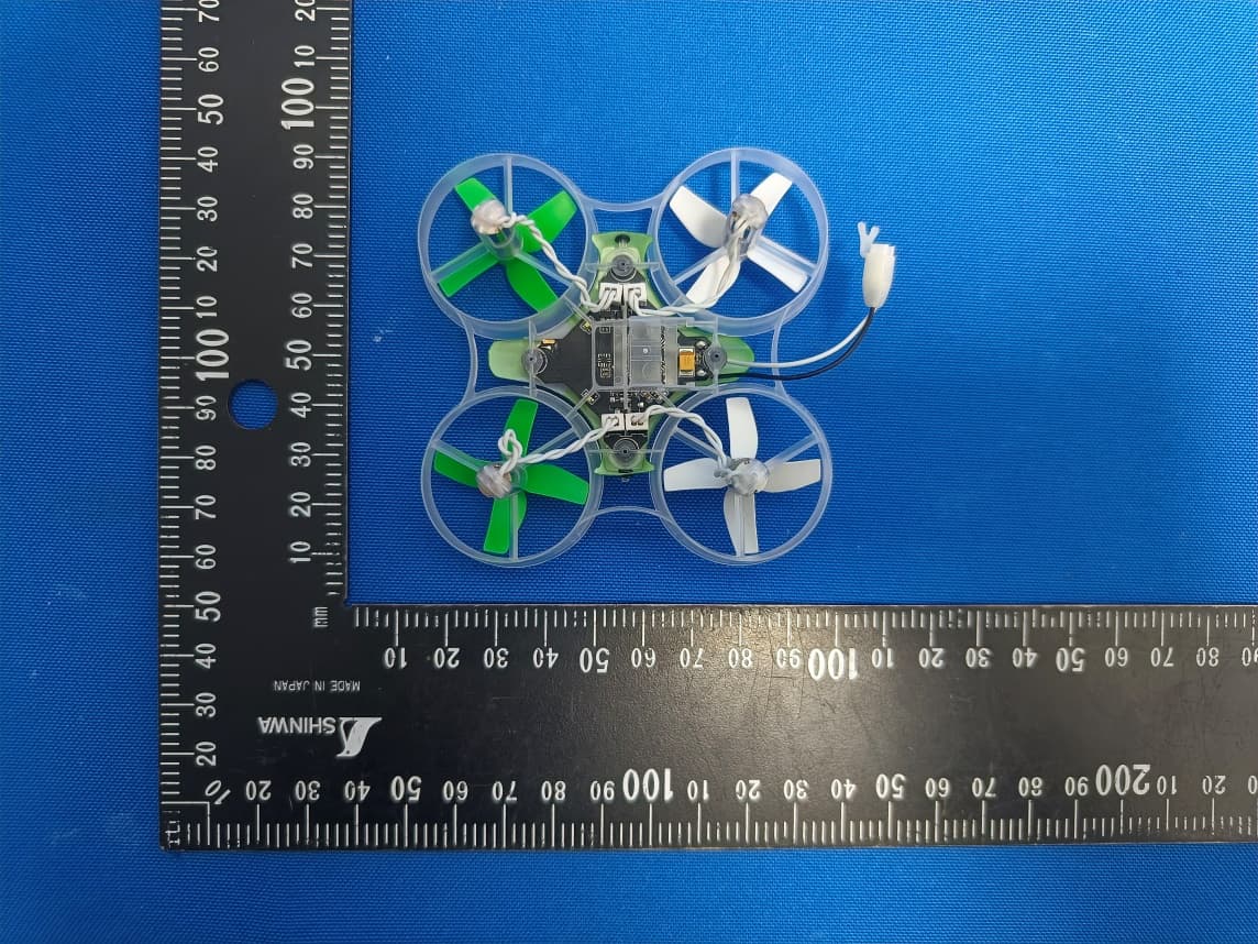
BRWBLH08701
Jul 29, 2023Inductrix RTF
Equipment Class
DTS - Digital Transmission System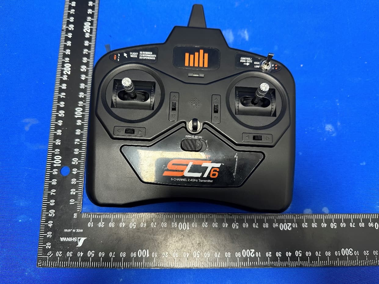
BRWSPMR1275
May 05, 2023SLT6
Equipment Class
DTS - Digital Transmission System
BRWSPMAR10360T
Oct 11, 2020AR10360T 10 Channel AS3X/SAFE Telemetry Receiver
Equipment Class
DSS - Part 15 Spread Spectrum Transmitter
BRWSPMAR10100T
Oct 11, 2020AR10100T 10 Channel Telemetry Receiver
Equipment Class
DSS - Part 15 Spread Spectrum Transmitter
BRWSPMSR6200A
Aug 11, 20206CH AVC surface receiver
Equipment Class
DXX - Part 15 Low Power Communication Device Transmitter