BRWXP7202Synthesized 7 Channel Radio Transmitter
Horizon Hobby, LLC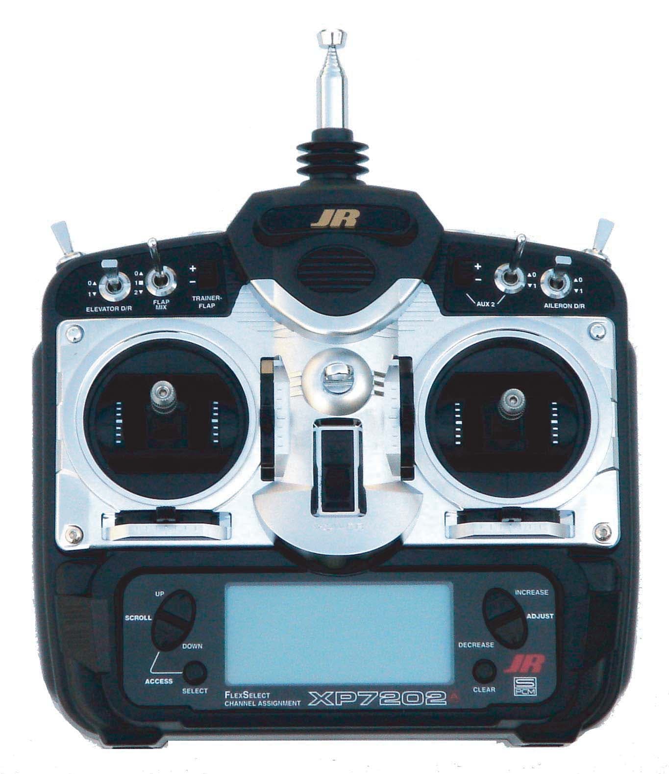
Click to zoom
Application Details
- Equipment Class
- TNB - Licensed Non-Broadcast Station Transmitter
- Date of Grant
- Jun 22, 2006
- Application Purpose
- Original Equipment
- Date of Application
- May 08, 2006
- Equipment Note
- Synthesized 7 Channel Radio Transmitter
- Frequency Range
- 72.01000000 - 72.99000000
- Company
- Horizon Hobby, LLC
- Country
- United States
Documents & Files
Document Text
Text extracted from the exhibit documents filed with the FCC. Open a document above to read the original.
Users Manual
Instruction Manual for Airplane and Helicopter XP7202 7- Channel synthesized computer radio 1- Using this manual In the front of this manual you will find the specifications for the transmitter and its included accessories. In addition, guidelines for installation have been included. For your convenience, this manual is arranged with a separate sections for airplane and helicopter software functions: Airplane Programming: Pages xx thru xx Helicopter Programming: Pages xx thru xx. Programming functions are discussed in the same order that they appear in the radio. An explanation of the use and purpose of each feature is provided, followed by an illustration of its LCD display. A blank data sheet has been included at the end of each section. Once all data has been input for a particular model, it is highly recommended that you also record it on a copy of the data sheet provided. If you should experience memory loss or want to make changes to the current settings, this step will save you a great deal of time. XP7202 Transmitter The XP7202 synthesized transmitter allows on screen channel selection of channels 15 thru channel 60 via the computer. The system prevents accidental turn-ons by requiring acknowledgement of the selected channel before a signal is transmitted. The system incorporates a hi- resolution dot matrix LCD display offering sophisticated graphics that are easy to read and understand. Two model type programming offers airplane and helicopter pilots programming options that will meet the most demanding modelers needs. Control sticks are adjustable for spring tension and length. Twenty-model memory storage capacity allows programming of up to twenty separate helicopters or airplanes or you can program more than one set-up for a single aircraft. Two versions of the transmitter are available: Airplane and Helicopter. The switch positions are optimized for each model type however the programming is identical in both versions. 3. Component Specifications 3A System Specifications Type Aircraft Helicopter System Name XP-7202A XP-7202H Transmitter Body NET-K237US NET-K237US Receiver NER-790 NER-790 Charger NEC-222 NEC-222 Airborne Battery 1100mAh 1100mAh Servos NES-821x4 NES-821x4 Accessories Standard Switch Standard Switch 12" Aileron Ext. 12" Aileron Ext. Charge Jack Charge Jack Servo Accys Servo Accys Hex Wrench Hex Wrench Instruction Manual Instruction Manual 3B Transmitter Specifications Type Aircraft Helicopter Model Number NET-G127US NET-G127US Encoder 7-Channel Computer System 7-Channel Computer System RF Module 72MHz 72MHz Modulation PCM (S or Z) or PPM PCM (S or Z) or PPM Output Power Approximately 750mw Approximately 750mw Current Drain 200mA (70mA with DSC) 200mA (70mA with DSC) Power Source 1.2Vx8 NiMh (9.6v) 15000mAh 1.2Vx8 NiMh (9.6v) 1500mAh Output Pulse 1000-2000 (1500 Neutral) 1000-2000 (1500 Neutral) 4. Battery Charging 4A Transmitter/Receiver Note: It is imperative that you fully charge both the transmitter and the receiver battery packs prior to each fly session. To do so, using the included wall charger, leave the charger and batteries connected overnight (16 hours). The first charge should be approximately 20-24 hours in order to fully charge both battery packs to peak capacity. The charger supplied with this system is designed to recharge your batteries at a rate of 150 mA for the transmitter and 120 mA for the receiver battery pack. Transmitter Polarity The center pin on all JR transmitters is negative. Therefore, the center pin on all JR chargers is negative, not positive. This is different from many other manufacturers chargers and radio systems. Beware of improper connections based on “color coded” wire leads, as they may not apply in this instance. You must make sure that the center pin of your JR transmitter is always connected to the negative voltage for correct polarity hookup. 4B Charger The pilot lamps should always be ON during the charging operation. If they’re not, check to make sure that both the transmitter and receiver are switched OFF. Do not use this charger for equipment other than JR. The charging plug polarity may not be the same and equipment damage can result. During the charging operation, the charger’s temperature is slightly elevated. This is normal. 5. General Information 5.1 Control Stick Length Adjustment the XP7202 allows you to adjust the control sticks’ length. Loosen Tighten To adjust the stick length, use the 2 mm Allen wrench (supplied with your XP7202 transmitter) to unlock the setscrew. Turn the wrench counterclockwise to loosen the screw. Then, turn the stick clockwise to shorten or counterclockwise to lengthen. After the control stick length has been adjusted to suit your flying style, tighten the 2 mm set screw. If you desire longer sticks, JR offers a longer stick tip (JRPA047) that is approximately one inch longer than the standard stick. This stick is available at your local JR dealer. 5.2 Control Stick Tension Adjustment Note: Remove the transmitter Nicad battery, and six (6) transmitter back cover screws as shown on the previous page. Remove the transmitter back, being careful not to cause damage to any components Adjust each stick tension screw for the desired tension (counterclockwise to loosen stick feel, clockwise to tighten stick feel). When adjusting the throttle ratchet tension, make sure the adjusting screw does not touch the PC board after the adjustment is complete. 5.4 DSC Cord For proper DSC hook up and operation: 1. Leave the transmitter power switch in the OFF position. The transmitter will not transmit radio frequency (RF) in this position. 2. Plug the DSC cord (optional) into the DSC port in the rear of the transmitter. 3. The encoder section of the transmitter will now be operational and the LCD display will be lit. 4. Plug the other end of the DSC cord into the receiver charge receptacle. Turn the switch harness to the ON position. Note: The DSC function will only operate with the JRPA001 Deluxe Swit…
Text truncated - open the document above for the full version.
Block Diagram
ANT Band Pass Filter Modulator Regulator 㪧㪣㪣 㪠㪚 㪣㪧㪝 VCO 㪙㪬㪉㪍㪊㪇㪛㪊㪒㪈㪪㪭㪉㪐㪇 㪙㫌㪽㪽㪼㫉 㪉㪪㪢㪏㪏㪉 㪙㫌㪽㪽㪼㫉 㪘㫄㫇㪅 㪠㪚 㪊 㪨㪈㪈㪒㪉㪪㪚㪋㪌㪈㪐 㪙㫌㪽㪽㪼㫉 㪉㪪㪢㪏㪏㪉 㪨㪈㪊 㪨㪈㪉㪒 㪨㪈㪒 㪨㪉㪒 㪨㪐㪃㪨㪈㪇 㪠㪚㪉㪒 㪉㪪㪢㪏㪏㪉 㪉㪪㪚㪋㪌㪈㪐 㪎㪏㪣㪇㪌㪝 㪒㪉㪪㪚㪋㪎㪊㪏㪰 㪛㪋 㪒㪈㪪㪭㪉㪐㪇 Power Amp 㪨㪊㪒 㪉㪪㪚㪋㪎㪊㪌 㪙㫌㪽㪽㪼㫉 㪘㫄㫇㪅 Power ON/OFF SW Q4,Q7 ;2SA1298 Q6,Q8 ;2SC4738 Crystal 13.0MHz 㪦㪽㪽㫊㪼㫋 㪛㪌㪒 㪟㪭㪚㪊㪌㪇㪙 RF Power ON-OFF 2SA1204/DTC114 DSC/ TRN TC4W53 2SA1204/DTC114 BZ System Control 12V CPU H8/HD64F3687FP Clock 13.6533MHz LCD VD4557AGRC LCD. PWM Cnt. 2SA1298 Channel 1~4 Stick Trim Channel 5-7 Edit key SW18 SW25 (Toggle Sw) Function Sw & PLL Controll data Modulation DTC114 Vcc FCC ID#BRWXP7202 Figure 5.1 Transmitter Schematic Diagram Page 9
External Photos
FCC ID# BRWXP7202 Page 14
ID Label/Location Info
FCC ID# BRWXP7202 Page 16
Internal Photos
FCC ID# BRWXP7202 Page 15
Operational Description
Page 4 Technical Report Transmitter Model XP7202 FCC ID# BRWXP7202 2.0 ENCODER THEORY OF OPERATION Reference is made to Figure 5.1, Transmitter Block Diagram. The functions of the encoder are to: * accept the analog voltages from the control inputs (joysticks, toggle switch). * process the analog voltages to create control mixing, adding, reversing, etc., as desired by the user. * sample these voltages in a cyclic rhythm under control of the system's internal timing generator. (This process is called commutation.) * process these analog voltages into binary weighted digital control words by means of an Analog-to-Digital Converter (ADC). * store these digital representations of the analog control input into a temporary memory (RAM). * supply this serial data stream to a buffer-driver for modulation of the RF Transmitter. * provide "housekeeping" of the encoding process by means of a quarts crystal controlled internal clock. * provide supply voltages to the RF section (Vcc = 9.6V battery voltage ; Vreg = 5.0V regulated voltage). The entire program which controls the timing housekeeping, parallel-to-serial conversion process, and insertion of synchronization words and error detection codes is governed by a Central Processing Unit (CPU) under control by an internally stored program residing in Read-Only Memory (ROM). The CPU, RAM and ROM are all part of a single-chip microprocessor. Resolution of the Analog-to-Digital conversion process is ten (10) bits for a control accuracy of 1:2 10
Operational Description
Page 6 Technical Report Transmitter Model XP7202 FCC ID# BRWXP7202 3.2 Block Diagram (Reference is made to Figure 5.1) The (up to) four control potentiometers are at the down left side of the schematic drawing. The control potentiometer, which is mechanically coupled to the control (joy) stick, is supplied with the regulated 5.0V voltage. The wiper on this pot is exactly centered in the neutral control stick position. All analog processing is performed as deviations from this center (reference) voltage. After the mixing of each channel, control voltage is changed to Pulse Train, through encoder circuit. The Q11(2SC4519)is an LC-type VCO(Voltage Controlled Oscillator), which is designed to oscillate with about 72.550MHz. Its output is led to amplifying stage for transmitting through a buffer(Q12),while it is also led to the PLL through a buffer(Q13). The pulses generated by the CPU are transferred to the VCO so as to modulate the radio wave. this part is strictly shielded from electric/magnetic noise. The IC3(BU2630F)is a PLL(phase Lock Loop). Exact 13.000MHz is generated by an internal crystal oscillator, and divided by 5,200 for 2.5kHz. VCO wave is also divided by a definite number, which is 29,004 in case of 72.510MHz,for getting 2.5kHz. Two 2.5kHz’s are compared in the phase and the VCO is so controlled that the error gets minimum, while the modulation is so fast that the filter between the PLL and the VCO cancels an error fluctuation. The set up of the frequency is done with Encoder unit. This frequency data is stored in the IC(H8/HD64F368FP) as an above-mentioned dividing number, and transferred to the PLL as the serial data while the transmitter is in normal operation mode. Frequency data can be changed only in system set-up mode with the power of the RF section being cut. Directly after it has turned on normally, though the CPU starts sending the PLL the data, the radio wave is still silent because the RF amplifier (Q1,Q2)is not supplied with the power yet. After a while, certain stabilizing time for the PLL, the Q4(2SA1298)starts to supply them with the power so that the radio wave is transmitted. Page 7 Technical Report Transmitter Model XP7202 FCC ID# BRWXP7202 The modulated signals supplied from Transmitter are PCM and PPM, and this modulated signal data is Set by IC(H8/ HD64F368FP). The modulated signal is conducted through phase-modulator, and the deviation value of the center frequency is fixed and changed by the wave form, symmetric in PCM and asymmetric in PPM. (For example, deviation in PCM is 0, the deviation in PPM is about 1.1KHz) This deviation value is supported by varying the impressed voltage to D6 (HVC350B). Q2 drives the Power Amplifier (PA). The straight-through PA stage(Q3) is followed by a matching and band pass/low-pass network. This network matches the low PA stage output impedance to the whip antenna. DC Supply Voltage enter the RF section: 12 Volt "law" battery voltage supplies the PA stage only. PLL stages, and bias current for all stages, including the PA, are derived from the regulated 5.0 Volt. 4.0 FAILURE ANALYSIS A failure analysis was conducted to ascertain that single-component failure will not result in unauthorized radiation. It should be noted that component failure would result in return of the unit to the factory, or to an authorized repair station. (Reference is made to Figure 5.2, Transmitter Schematic Diagram) Failure of any of the transistors (predominant failure mode: emitter-collector short) will result in the unit becoming inoperative: In the case of Q11 oscillator short, RF output will be non-existent. Q12,Q1,Q2 or Q3 failure will result in very low, if any, output. Failure of the MOD IN input (latch at 0 or 12 Volt) or modulator transistor Q9, Q10 and variable diode D4 (open or short) will result in carrier frequency. Although this failure would render the unit inoperative, the frequency tolerance would still fall within the channel bandwidth and tolerance requirements of .002% of 72 MHz = 1.44 KHz. When PLL circuit is broken, for example, crystal X1 break down, or IC101(BU2630) for PLL is broken, PLL will stop functioning. All other incidental failures will render the unit inoperative and because for return of the transmitter to the service facility.
Schematics
7 1 P 2 1 P / 5 N A ) 2 / 2 ( - X X X X 7 X e e S 0 1 P 5 1 P 4 1 P 7 6 P 6 6 P c c V 1 1 P 6 1 P 2 6 P 1 6 P N O - F R r e w o P N O I M N t e s e R 6 5 4 3 2 1 B 4 N C /AN6 PB6 PB7/AN7 AVcc X2 X1 VCL TEST Vss OSC2 OSC1 Vcc P51/WKP1 P34 P35 RES 6 3 P 7 3 P 2 P K W / 2 5 P 3 P K W / 3 5 P 4 P K W / 4 5 P G R T D A / 5 P K W / 5 5 P W O M T / 0 1 P M W P / 1 1 P 2 1 P /FTIOD0 P63 A D S / 6 5 P 4 2 P L C S / 7 5 P V I R M T / 4 7 P V O M T / 6 7 P V I C M T / 5 7 P P62/FTIOC0 P61/FTIOB0 NMI P60/FTIOA0 P64/FTIOA1 P65/FTIOB1 P66/FTIOC1 P67/FTIOD1 P85 P87 P86 P20/SCK3 P21/RXD 7 8 6 3 / 8 H P50/WKP0 P22/TXD 0 7 P 2 _ 3 K C S / P23 5 N A / 5 B P 0 N A / 0 B P 4 N A / 4 B P 1 3 P 3 N A / 3 B P 2 N A / 2 B P 1 N A / 1 B P 2 3 P 3 3 P V G R T / 3 Q R I / 7 1 P 2 Q R I / 6 1 P 1 B I M T / 1 Q R I / 5 1 P 0 Q R I / 4 1 P 2 _ D X T / 2 7 P 2 _ D X R / 1 7 P 0 3 P 1 2 3 4 5 6 7 8 9 10 11 12 13 14 15 16 7 1 8 1 9 1 0 2 1 2 2 2 3 2 4 2 5 2 6 2 7 2 8 2 9 2 0 3 1 3 2 3 33 34 35 36 37 38 39 40 41 42 43 44 45 46 47 48 9 4 0 5 1 5 2 5 3 5 4 5 5 5 6 5 7 5 8 5 9 5 0 6 1 6 2 6 3 6 4 6 U P C D U R 4 R V - 7 W S + 8 W S 6 5 4 3 2 1 B 3 N C ) 2 ( H T / ) 1 ( E L E 3 R V - 5 W S + 6 W S 6 5 4 3 2 1 B 2 N C L I A 2 R V - 3 W S + 4 W S ) 2 ( E L E / ) 1 ( H T 1 R V - 1 W S+ 2 W S 104 C12 104 C11 1K R14 1K R15 1K R8 1K R9 2 0 1 4 C 2 0 1 3 C 2 0 1 2 C 2 0 1 1 C 3 0 1 5 C 2 0 1 3 2 C 2 0 1 2 2 C 2 0 1 1 2 C 2 0 1 4 2 C 1K R2 1K R1 1K R6 1K R3 1K R4 1K R7 1K R5 2 0 1 1 3 C 2 0 1 0 3 C 2 0 1 9 2 C 2 0 1 8 2 C 12 6 1 N C T T A B 12 5 1 N C 12 1 2 3 K J C D 2 K J W S r e w o P N O 103C84 1234567 CN7B 1 8 C I 5 0 L 8 7 + C83 33u 103 C81 103 C82 + C80 22u D83 1SR35 D82 1SR35 1 8 Q A U E 4 1 1 C T D 2 8 Q A U E 4 1 1 C T D 1 Z B 102C85 102C86 2.2K R82 2.2K R81 1 C I A A 0 4 L V 5 H R 103C33 102C35 4.7K R32 7.5K R33 10K R31 100K R29 K 2 . 2 0 3 R 1 D 2 5 3 223C36 + C37 1u JPC R46 5 Q w 4 0 2 1 A 3 0 1 2 5 C K 2 2 7 4 R 6 Q DTC114EUA 103C51 123 CN9 RF 102C48 103C49 1 Q w 4 0 2 1 A 3 0 1 0 4 C K 2 . 2 9 3 R K 2 2 8 3 R 2 Q A U E 4 1 1 C T D 103C39 102C53 102C41 10K R35 104C34 A U E 4 1 1 C T D 4 Q 1234567 CN7 1234 CN14 104C6 104 C7 103C44 22K R44 K 1 2 4 R 470K R43 102C46 102C47 3 Q w 4 0 2 1 A 1 2 3 5 4 6 78 h n I e e V A s s V 0 h C 1 h C d d V m o C U F 3 5 W 4 C T 2 C I 102C43 + 2 4 C u 0 1 100K R37 K 0 0 1 6 3 R p 3 3 8 C p 3 3 9 C 1 X 22K R34 F1 FUSE 1 8 D 2 5 3 A U E 4 1 1 C T D 7 Q 1K R71 1K R70 1K R69 1K R68 1K R67 1K R66 105C54 105C55 105C56 105C57 105C58 105C59 105C60 105C61 105C62 104C63 3V D2 103C38 2.2K R48 2.2K R45 3 0 1 5 6 C K 2 . 2 1 4 R K J C S D 1 K J 1K R19 1K R18 1K R17 1K R16 1K R23 1K R22 1K R21 1K R20 1K R24 1K R28 1K R27 1K R26 6 5 4 3 2 1 B 1 N C 2 0 1 5 4 C 2 0 1 0 5 C 4 3 2 1 T O O B 1 1 N C 2 0 1 8 6 C 2 0 1 7 6 C 2 0 1 6 6 C 2 0 1 0 7 C 2 0 1 9 6 C 2 0 1 9 1 C 2 0 1 8 1 C 2 0 1 7 1 C 2 0 1 6 1 C 3 0 1 0 2 C R56 10K R57 10K R58 10K R59 10K R13 10K R12 10K R11 10K R10 10K R60 10K R61 10K R62 10K 6 5 4 3 2 1 2 1 N C ) G O R P ( F R - L L P 820 R40 C14 104 C13 104 R63 10K 1A 1Y 2A 2Y 3A 3Y 4A 4Y 5A 5Y 6A 6Y GND Vcc 1 2 3 4 5 6 78 9 10 11 12 13 14 3 C I A 7 0 V L 4 7 D H 5 5 R 0 8 6 + C64 10u R53 10K R52 10K 10K R54 10K R51 10K R50 1K R72 1K R73 R A E L C 8 1 W S T C E L E S 9 1 W S P U 0 2 W S N W O D 1 2 W S C E D 3 2 W S C N I 2 2 W S 4 2 W S 5 2 W S 1 2 3 4 5 6 7 8 9 0 1 1 1 2 1 3 1 4 1 5 1 6 1 7 1 8 1 9 1 0 2 D C L 0 1 N C 10K R65 10K R64 R49 3.3K 1234 CN8 1234 B 8 N C 9 8 7 6 5 4 3 2 1 2 1 1 1 0 1 3 N C 9 8 7 6 5 4 3 2 1 2 1 1 1 0 1 1 N C 1K R25 2 0 1 2 3 C 2 0 1 5 2 C 2 0 1 6 2 C 7 6 5 4 3 2 1 T F E L 6 N C JP2 JP1 JP4 JP3 7 6 5 4 3 2 1 T H G I R 5 N C JP5 JP6 JP7 JP8 3 1 P J JP9 JP11 JP10 4 1 P J 2 0 1 7 2 C 5 1 P J 2 1 P J C10 104 C15 104 FCC ID# BRWXP7202 Figure 5.2.1. Transmitter Schematic Diagram Page 10 5 N A c c V 7 1 P 1 1 P 6 1 P D N G 2 6 P 1 6 P 2 1 P 0 1 P 5 1 P 4 1 P D N G 7 6 P 6 6 P 7 6 5 4 3 2 1 7 6 5 4 3 2 1 5 P J 6 P J 3 P J 0 1 P J 1 P J 2 P J 7 P J 8 P J 3 1 P J 4 1 P J 5 1 P J 4 P J 1 1 P J 9 P J 6 1 P J 2 1 P J -+ R / D - D U R R / D - L I A 7 6 5 4 3 2 1 -+ X I M - P A L F R A E G R / D - E L E 7 6 5 4 3 2 1 FCC ID# BRWXP7202 Figure 5.2.2. Transmitter Schematic Diagram Page 11 D N G * * * H u 7 1 . 0 V 5 V 5 S X 4 S A 3 0 H R R E T U P M O C T S O H O T 6 3 2 1 4 6 4 3 2 1 T U O N I D O M c c V 3.3uH L7 12K R5 3.3K R6 R7 22 R8 33 9 R 0 2 2 1 1 R 5 1 R10 3.3K 3 Q 0 1 9 4 C S 2 R14 6.8 R13 6.8 R15 470 8 1 C P 0 3 H C C20 CH100P C23 CH82P C15 103 C14 102 P 0 5 1 H C 1 1 C T N A 103 C2 P 7 4 H C 3 C 103 C7 9 3 R K 3 . 3 1 P K 1 R38 820 0 1 Q Y 8 3 7 4 C S 2 R36 39 R35 15K 3 3 R K 9 3 9 Q Y 8 3 7 4 C S 2 C51 102 1 3 R K 0 1 000 C12 C55 B472 W P J 4 R B 9 N C C17 CH68p R44 180 1 1 Q 6 - 9 1 5 4 C S 2 C67 CH68P D3 1SV290 1 5 R K 2 . 2 C79 10uF6.3V Tantalum CH82P C66 12K R42 10K R41 P 3 H C 3 7 C 33 R45 102 C70 CH1P C72 K 0 1 4 5 R B473 C81 1SV290 D4 CH2P C68 47K R43 1 Q 2 8 8 K S 2 10K R2 R32 10K C34 7 3 R 0 8 1 C1 CH5p C52 B471 R12 6.8 103 C4 R52 47 R53 6.8k 2 6 C F P 4 J U 3 1 Q 2 8 8 K S 2 1K R50 CH47P C78 6 - 9 1 5 4 C S 2 2 Q 102 C5 R34 NON K 0 0 1 9 4 R C75 PAT NON C77 000 J 2 8 1 B 3 5 C D5 HVC350B 7 8 C p 6 5 J U 7 5 R K 0 0 1 F 5 0 L 8 7 2 C I NON C56 103 C58 105 C57 10uF6.3V C59 CH1P C6 7 2 C 3 0 1 p 5 1 H C 1 2 C 1 L S 2 7 - S T 000 C54 L11 0.22uH 56K R47 0 8 6 6 4 R 2 8 8 K S 2 2 1 Q 560 R48 P 2 2 H C 4 7 C 0 2 2 1 R 3 6 C P 7 H C 10K R18 103 C37 6pF VC2 4 6 C P 2 1 H C 10uF6.3V Tantalum C89 B105 C88 K 3 . 3 8 5 R 47K P2 C60 104 pat non C61 R40 47k C90 103 W P J 3 J 9 1 1 C S H 7 D 3 6 R K 0 1 5 6 R K 0 1 4 6 R K 0 1 R3 33 C31 103 C30 4 Q Y 8 9 2 1 A S 2 6 1 R K 7 4 C35 6 Q Y 8 3 7 4 C S 2 103 C32 R17 10K 5 2 R K 0 1 C39 104 R24 10K C44 P 2 1 H C 5 6 C C82 103 K C T U O X N I X s s V D P R R - P N O R R - F E C D D V D P T P - T N O T T - F D L A D BU2630F 1 2 3 4 5 6 7 9 8 0 1 1 1 2 1 3 1 4 1 5 1 6 1 3 C I 1 X z H M 0 0 . 3 1 UJ5p C86 C85 UJ15p 8 L 1 0 6 W H 0 8 C 1 7 4 B 2 L S 2 7 - S T T 6 - P T 4 L T 7 - P T 5 L 6 L T 4 - P T F P 6 1 C V L14 JPW L12A JPW A 5 1 L 0 …
Text truncated - open the document above for the full version.
Test Report
A-009-06-C Page 1 of 21 KEC Ikoma Testing Laboratory 12128 Takayama-cho Ikoma-city Nara 630-0101 Japan KANSAI ELECTRONIC INDUSTRY DEVELOPMENT CENTER HEAD OFFICE IKOMA TESTING LABORATORY 6-8-7 NISHITENMA 12128 TAKAYAMA-CHO KITA-KU OSAKA 530-0047 JAPAN IKOMA-CITY NARA 630-0101 JAPAN Corporate Juridical Person TEST REPORT Report No. A-009-06-C Date: 18 April 2006 This test report is to certify that the tested device properly complies with the requirements of: FCC Rules and Regulations Part 95 : Radio Control (R/C) Radio Service. The tests necessary to show compliance to the requirements were performed and these results met the specifications of requirement. The results of this report should not be construed to imply compliance of equipment other than that, which was tested. Unless the laboratory permission, this report should not be copied in part. 1. Applicant Company Name : JAPAN REMOTE CONTROL CO., LTD. Mailing Address : 2-2-12 EIWA, HIGASHIOSAKA-CITY, OSAKA, 577-0809 JAPAN 2. Identification of Tested Device Type of Device : Radio Control (R/C) Transmitter Kind of Equipment Authorization : : DoC : Certification : Verification FCC ID : BRWXP7202 Device Name : FM 7-CHANNEL TRANSMITTER Trade Name : JR PROPO Model Number : XP7202 Serial Number : Prototype No.1 : Production : Pre-production : Prototype Date of Manufacture : March 2006 3. Test Items and Procedure : RF Power Output (Substitution Method) : Modulation Characteristics : Emission Bandwidth : Spurious Radiation (Substitution Method) : Frequency Stability Measurement Above all tests were performed under: FCC Part 2 Sec2.1046, Sec2.1047, Sec2.1049, Sec2.1053, Sec2.1055 and Sec2.1057. : without deviation, : with deviation (details are found inside of this report) 4. Date of Test Receipt of Test Sample : 23 March 2006 Condition of Test Sample : : Damage is not found on the set. : Damage is found on the set. (Details are described in this report) Test Completed on : 12 April 2006 Seiichi Izumi General Manager of Ikoma Testing Laboratory A-009-06-C Page 2 of 21 KEC Ikoma Testing Laboratory 12128 Takayama-cho Ikoma-city Nara 630-0101 Japan Table of Contents 1. GENERAL INFORMATION .......................................................................................................................... 3 1.1. Product Description...................................................................................................................................... 3 1.2. Description for Equipment Authorization .................................................................................................... 3 1.3. Test Facility ................................................................................................................................................. 3 2. TESTED SYSTEM........................................................................................................................................... 4 2.1. Test Mode .................................................................................................................................................... 4 2.2. Block Diagram of EUT System.................................................................................................................... 5 2.3. List of EUT System...................................................................................................................................... 5 2.4. List of Antenna............................................................................................................................................. 5 3. RF OUTPUT POWER AND RADIATED SPURIOUS EMISSIONS .......................................................... 6 3.1. Reference Rule and Specification ................................................................................................................ 6 3.2. Test Procedure.............................................................................................................................................. 6 3.3. Test Configuration ....................................................................................................................................... 7 3.4. Photographs of EUT System Configuration................................................................................................. 9 3.5. Test Results ................................................................................................................................................ 11 4. MODULATION CHARACTERISTICS ......................................................................................................12 4.1. Reference Rule and Specification .............................................................................................................. 12 4.2. Test Results ................................................................................................................................................ 12 5. EMISSION BANDWIDTH ........................................................................................................................... 13 5.1. Reference Rule and Specification ............................................................................................... ............... 13 5.2. Test Configuration ..................................................................................................................................... 13 5.3. Test Results ................................................................................................................................................ 14 6. FREQUENCY STABILITY MEASUREMENT .......................................................................................... 18 6.1. Reference Rule and Specification .............................................................................................................. 18 6.2. Frequency vs Temperature Test ................................................................................................................. 18 6.3. Frequency vs …
Text truncated - open the document above for the full version.
Contact Information
Applicant
Jason Rosa(Lead Quality and Compliance Associate)
Technical Contact
Horizon Hobby IncPeter R Bergstrom
[email protected]217-403-3202
4105 Fieldstone Rd · Champaign, Illinois · United States
Non-Technical Contact
Horizon Hobby inc.Peter R Bergstrom
[email protected]217-403-3202
Test Firm
Kansai Elec. Ind. Dev. Ctr. Ikoma TestTeru Kawahara
Technical Specifications
| # | Rule Parts | Frequency Range | Power Output | Emission | Tolerance |
|---|---|---|---|---|---|
| 1 | 95A | 72.01 MHz - 72.99 MHz | 114.82 mW | F1D | 0.0020000000 % |
Other Applications from Horizon Hobby, LLC
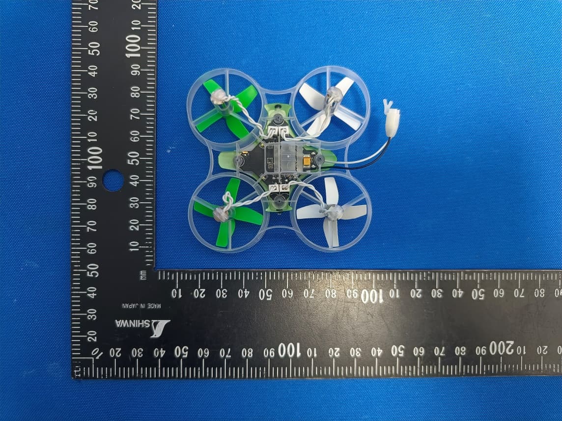
BRWBLH08701
Jul 29, 2023Inductrix RTF
Equipment Class
DTS - Digital Transmission System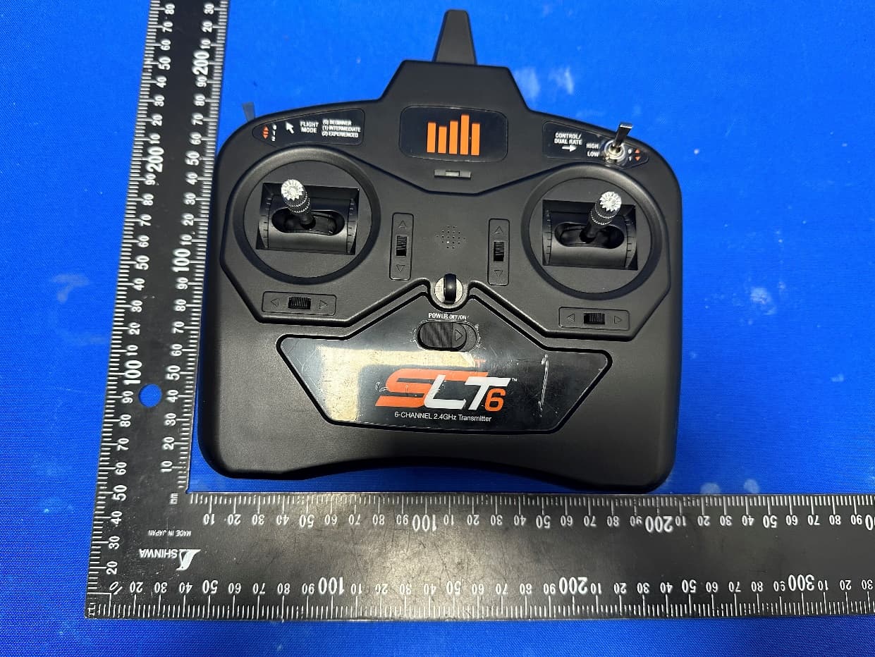
BRWSPMR1275
May 05, 2023SLT6
Equipment Class
DTS - Digital Transmission System
BRWSPMAR10360T
Oct 11, 2020AR10360T 10 Channel AS3X/SAFE Telemetry Receiver
Equipment Class
DSS - Part 15 Spread Spectrum Transmitter
BRWSPMAR10100T
Oct 11, 2020AR10100T 10 Channel Telemetry Receiver
Equipment Class
DSS - Part 15 Spread Spectrum Transmitter
BRWSPMSR6200A
Aug 11, 20206CH AVC surface receiver
Equipment Class
DXX - Part 15 Low Power Communication Device Transmitter