DBZUT400WIRELESS MICROPHONE TRANSMITTER
Lectrosonics Inc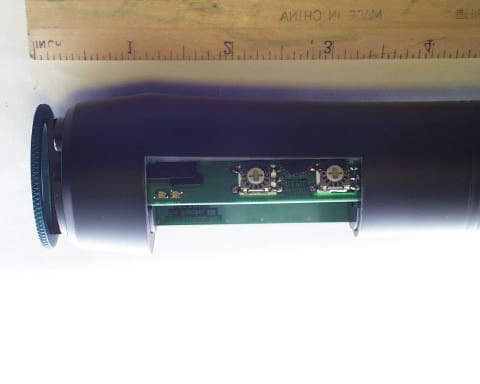
Click to zoom
Application Details
- Equipment Class
- TBF - Licensed Broadcast Transmitter Held to Face
- Date of Grant
- Oct 06, 2003
- Application Purpose
- Original Equipment
- Date of Application
- Oct 06, 2003
- Equipment Note
- WIRELESS MICROPHONE TRANSMITTER
- Frequency Range
- 614.00000000 - 793.50000000
- Company
- Lectrosonics Inc
- Country
- United States
Documents & Files
Document Text
Text extracted from the exhibit documents filed with the FCC. Open a document above to read the original.
Users Manual
UT400 DIGITAL-HYBRID FREQUENCY-AGILE HAND-HELD TRANSMITTER OPERATING INSTRUCTIONS and trouble-shooting guide LECTROSONICS, INC. Rio Rancho, NM www.lectrosonics.com 2 UT400 LECTROSONICS, INC. TABLE OF CONTENTS INTRODUCTION..................................................................................................... 3 GENERAL TECHNICAL DESCRIPTION ................................................................. 4 CONTROLS AND FUNCTIONS .............................................................................. 6 VARIMIC CONTROLS ............................................................................................. 7 BATTERY INSTALLATION ....................................................................................... 9 OPERATING INSTRUCTIONS............................................................................... 10 OPERATING NOTES ............................................................................................. 11 ADJUSTING THE TRANSMITTER FREQUENCY ................................................. 11 TROUBLESHOOTING............................................................................................ 12 SPECIFICATIONS ................................................................................................. 13 SERVICE AND REPAIR ......................................................................................... 14 RETURNING UNITS FOR REPAIR ........................................................................ 14 WARRANTY............................................................................................ Back cover 3 Rio Rancho, NM - USA Digital-hybrid, Frequency Agile Handheld Transmitter INTRODUCTION Thank you for selecting the Lectrosonics UT400 hand-held wireless transmitter. The UT combines over 80 years of engineering experience with the very latest components in a design that addresses the most demanding professional applications. The design of the UT400 was the direct result of numerous conversations with users, staging and touring companies and dealers across the US. The specific concerns and needs brought up in these conversations led directly to the development of the opera- tional features offered on the UT400. Two hundred fifty six frequencies are user selectable in 100kHz steps to alleviate interference problems in travelling venues The UT400 is an integral microphone/transmitter with an internal antenna. The antenna is a dipole type utilizing the two printed circuit boards as the elements. The housing is composed of durable PVC, machined to a natural, comfortable shape. Internal me- chanical parts are machined aluminum and brass. Only the UT400 transmitters are covered in this manual. Companion receivers are covered in separate manuals. The UT400 will operate with any 100 Series, 200 Series and 400 Series Lectrosonics receiver in the same frequency group. 4 UT400 LECTROSONICS, INC. GENERAL TECHNICAL DESCRIPTION GENERAL The 400 system uses 75kHz wide deviation for an extremely high signal to noise ratio. The switching power supplies provide constant voltages to the transmitter circuits from the beginning (9.3 Volts) to the end (5.5 Volts) of battery life. The input amplifier uses an ultra low noise op amp for quiet operation. It is gain controlled with a wide range dual envelope input compressor which cleanly limits input signal peaks over 30dB above full modulation. DIGITAL HYBRID TECHNOLOGY All wireless links suffer from channel noise to some degree, and all wireless microphone systems seek to minimize the impact of that noise on the desired signal. Conventional analog systems use compandors for enhanced dynamic range, at the cost of subtle artifacts (known as “pumping” and “breathing”). Wholly digital systems defeat the noise by sending the audio information in digital form, at the cost of some combination of power, bandwidth and resistance to interfer- ence. The Lectrosonics Digital Hybrid system overcomes channel noise in a dramatically new way, digitally encoding the audio in the transmitter and decoding it in the receiver, yet still sending the encoded information via an analog FM wireless link. This proprietary algorithm is not a digital implementation of an analog compandor but a technique which can be accomplished only in the digital domain, even though the inputs and outputs are analog signals. (As of this writing, the patent is still pending, so we cannot reveal detailed information about the algorithm at this time.) Channel noise still has an impact on received signal quality and will eventually overwhelm the receiver. The Digital Hybrid simply encodes the signal to use a noisy channel as efficiently and robustly as possible, yielding audio perfor- mance that rivals that of wholly digital systems, without the power and bandwidth problems inherent in digital transmis- sion. As always, these advantages come at a cost. The Digital Hybrid system requires fairly intensive digital processing in both the transmitter and the receiver. These processors cost money, take up space and consume power. The Digital Hybrid system also requires that the underlying RF link be of excellent quality, with better frequency re- sponse and distortion characteristics than that required by conventional systems. Because it uses an analog FM link, the Digital Hybrid enjoys all the benefits of conventional FM wireless systems, such as excellent range, efficient use of RF spectrum, and long battery life. However, unlike conventional FM sys- tems, the Digital Hybrid has done away with the analog compandor and its artifacts. Phase Locked Loop Voltage Controlled Oscillator Freq Switches 11001001 A-D Converter Digital Signal Processor 11001001 D-A Converter Shunt Limiter Bicolor Modulation LEDs Microprocessor 9V Battery Switching Power Supply +3.3v +1.8v +9v -3v Audio Encoded Audio + Pilot Tone 11.3 MHz Reference Bicolor Power LED Audio Level Input Amp Final Amplifier 50 Isolator Preamp Mic Element Preamp Level Tone 5 Rio Ran…
Text truncated - open the document above for the full version.
Block Diagram
ROGERS LABS, INC. LectroSonics Inc. 4405 W. 259th Terrace MODEL: UT400 Louisburg, KS 66053 Test #: 030924 FCCID#: DBZ UT400 Phone/Fax: (913) 837-3214 Test to: FCC Parts 2 and 74 Page 1 of 1 DBZUT400BlkDia.doc 9/25/2003 Block Diagram for UT 400.
Cover Letter(s)
September 25, 2003 Timco Engineering Inc. 849 NW State Road 45 Newberry, FL 32669 Office of Engineering and Technology Federal Communications Commission Columbia, MD 21046 Applicant: Lectrosonics, Inc. 581 Laser Road Rio Rancho, NM 87124 FRN 0007-0674-81 Re: Confidentiality for submittal information regarding FCC ID number DBZ UT400 PRODUCT: Wireless Microphone transmitter operating under part 74. Dear Sirs: Lectrosonics, Inc. requests that the material in the Printed Circuit Board Layout, Schematics, and Operational Description be withheld from public disclosure in accordance with Section 0.459 of the Commissions Rules, 47 C.F.R. 0.459 (1998), following grant of the application. In support of this request, Lectrosonics, Inc. submits the following: 1. Identification of the specific information for which confidential treatment is sought: The materials set fourth in the Operational Description, Printed Circuit Board layout, and Schematics, which are segregated from the non-confidential exhibits of the application, are those for which confidentiality is sought. 2. Identification of the Commission proceeding in which the information was submitted or a description of the circumstances giving rise to the submission: The proceeding is that involving the application for equipment authorization (certification) under FCC ID No: DBZ UT400 3. Explanation of the degree to which the information is commercial or financial, or contains a trade secret or is privileged: This material includes a detailed theory of operation, circuit diagrams, (schematic diagrams) and detail printed circuit board layout. As such, this material is treated as highly confidential business information. ROGERS LABS, INC. 4405 West 259 th Terrace Louisburg, KS 66053 4. Explanation of the degree to which the information concerns a service that is subject to competition: The material for which confidentiality is sought is employed in the design and manufacture of this transmitting equipment that is offered on a highly competitive basis. Customers for this equipment have a variety of competing sources. 5. Explanation of how disclosure of the information could result in substantial competitive harm: Disclosure would, in effect, give away the fruits of the labors of Lectrosonics, Inc.’s engineering personnel, who have designed the equipment and the manufacturing process. Disclosure would also offer competitors additional unwarranted insight into the state of the product development, thereby allowing competitors an advantage, not available to Lectrosonics, Inc. 6. Identification of any measures taken by the submitting party to prevent unauthorized disclosure: The information for which confidential treatment is sought is kept confidential by Lectrosonics, Inc. and not made available to third parties except pursuant to non-disclosure agreements. 7. Identification of whether the information is available to the public and the extent of any previous disclosure of the information to third parties: To the knowledge of those preparing this application, the information has not been disclosed publicly heretofore. While the general theory of operation of this equipment has been the subject of numerous disclosures in industry and standards groups as well as in rule making proceedings of the FCC, the protection sought is narrowly drawn and pertains to certain specific implementations of this radio technology. 8. Justification of the period during which the submitting party asserts that the material should not be available for public disclosure: This material should not be disclosed for at least 25 years. While improvements in design are made relatively frequently, disclosure of the design information would lead to insights into both design and manufacturing techniques that could have an adverse competitive effect for many years to come. This equipment is designed for commercial, industrial, and governmental applications. As such, unlike most consumer equipment, this equipment could be used for more than a decade in some cases. As such, it is important that the design not be made available to unauthorized persons who might attempt to use knowledge of the design to compromise the applications for which the equipment will be employed. Should you require any further information, please contact the undersigned. Thank you for your consideration in this matter. Sincerely, Scot Rogers
Cover Letter(s)
September 25, 2003 Timco Engineering Inc. 849 NW State Road 45 Newberry, FL 32669 Federal Communications Commission Equipment Approval Services P.O. Box 35815 Pittsburgh, PA 15251-3315 Applicant: Lectrosonics, Inc. 581 Laser Road Rio Rancho, NM 87124 FRN: 0007-0674-81 Equipment: FCC ID: DBZ UT400 FCC Rules: Part 2 and 74 Gentlemen: The 731 form and application have been electronically submitted and any attachments will be up loaded to your web site to be used in obtaining a grant of certification. It is requested that the information contained in the printed circuit board layout, operational description, and schematics of the application be held confidential per Section 0.459. A statement of confidentiality will be attached with the application at the time of submittal. The special fee for request of confidentiality will be submitted with the application. Should you require any further information, please contact the undersigned. Thank you for your consideration in this matter. Sincerely, Scot Rogers Rogers Labs, Inc. Enclosures ROGERS LABS, INC. 4405 West 259 th Terrace Louisburg, KS 66053 Phone / Fax (913) 837-3214
External Photos
ROGERS LABS, INC. LectroSonics Inc. 4405 W. 259th Terrace MODEL: UT 400 Louisburg, KS 66053 Test #: 030924 FCCID#: DBZ UT400 Phone/Fax: (913) 837-3214 Test to: FCC Parts 2 and 74 Page 1 of 2 DBZUT400Photos.doc 9/25/2003 Equipment photographs for UT 400. ROGERS LABS, INC. LectroSonics Inc. 4405 W. 259th Terrace MODEL: UT 400 Louisburg, KS 66053 Test #: 030924 FCCID#: DBZ UT400 Phone/Fax: (913) 837-3214 Test to: FCC Parts 2 and 74 Page 2 of 2 DBZUT400Photos.doc 9/25/2003
ID Label/Location Info
ROGERS LABS, INC. LectroSonics Inc. 4405 W. 259th Terrace MODEL: UT400 Louisburg, KS 66053 Test #: 030924 FCCID#: DBZ UT400 Phone/Fax: (913) 837-3214 Test to: FCC Parts 2 and 74 Page 1 of 1 DBZUT400Label.doc 9/25/2003 FCC ID label information for UT 400.
Internal Photos
ROGERS LABS, INC. LectroSonics Inc. 4405 W. 259th Terrace MODEL: UT400 Louisburg, KS 66053 Test #: 030924 FCCID#: DBZ UT400 Phone/Fax: (913) 837-3214 Test to: FCC Parts 2 and 74 Page 1 of 1 DBZUT400IntPhoto.doc 9/25/2003 Internal construction photographs for UT400, please refer to schematics for printed circuit board layout and component placements.
Parts List/Tune Up Info
LECTROSONICS TEST & ALIGNMENT PROCEDURE 1 MODEL: UT400 REV: 173232A (Main board) DATE: 25 September 2003 PAGE: 1 of 3 REV: 17333A (Logic Board) Firmware Ver: 1.0 Setup: Logic Board connected to RF Board. 9.0VDC in at RF board measured at battery contacts. Power Switch (SW3) On (Upper) position. Frequency “FF” selected at Logic Board SW1 and SW2. Output RF connected through a connector to P1, P2. MEASUREMENT. TEST CONDITIONS TYPICAL MEASUREMENT RESULT Program Processor: Program Microprocessor and apply label (FACTORY ONLY). Note that audio LED’s, D5 and D6 will begin flashing RED. This condition is normal and represents the condition Of PLL not locked. This will occur until the Block Information is programmed into the Logic Board. Program Frequency Block Number: Short Logic Board J7 pin 1 to pin 7. Position Frequency Select switches on Logic Board SW1 and SW2 to desired frequency block (SW1 = MSD, SW2 = LSD). Remove J7 short. This step may also be performed using the LECSET apparatus (does not require J7 short or SW1, SW2 manipulation). Frequency "FF" selected at SW1, SW2 of Logic Board after setting frequency block. Current Draw. 40 to 50 mA PLL Unlocked 65 to 85 mA PLL Locked DC Voltage Measurements: Measure DC Voltage at: TP30 + 1.8 VDC, +/- 100mV J5 Pin 6 +3.3VDC, +/- 200mV TP29 -3 VDC, +/- 200 mV Power Up LED Test. Power D.U.T. down and back up. Observe operation of LED’s D5, D6 and D7 as follows: At power up: All 3 LED’s flash RED After less than 1 second: All 3 LED’s flash GREEN After less than 1 second: All 3 LED’s OFF After approximately 1 second: D5 and D6 flash GREEN 4 times, then OFF After approximately 1 second: D7 continuous GREEN Power LED Test: Reduce input VDC at Battery Contacts. Observe operation of Power LED D2. +7.3 VDC: LED turns RED +6.8 VDC: LED flashes RED Output Power, Frequency, Pilot Tone and VCO Verification: Measure FF carrier signal power at RF Board P1, P2. +19 to +20 dBm Short Logic Board J7 pin 1 to pin 7. Adjust Logic Board SW2 to achieve proper carrier frequency at Main Board P1. FF frequency +/- 2 kHz Remove short. Return Logic Board SW2 to F position. Momentarily interrupt power at Main Board. Measure Pilot Tone level and frequency. -5.0 to -4.0 dBV, 25.136 Khz +/- 2 H Set Logic Board SW1 and SW2 to 00 position Momentarily interrupt power at Main Board. Measure 00 carrier signal power at Main Board P1. +19 to +20 dBm Measure 00 carrier frequency at Main Board P1. 00 frequency +/- 2 Khz Measure Pilot Tone level and frequency. -5.0 to –4.0 dBV, 32.000 Khz +/- 2 Hz Move Logic Board SW1 to position 8 (use 100 MHz span, 80 ctr). Measure frequency change (1.6 MHz), power and stability at each switch position. Move Logic Board SW2 to position 8. Measure frequency change (0.1 MHz) Return SW2 to F position. Momentarily interrupt power at Main Board Measure 80 carrier signal power at Main Board P1. +19 to +20 dBm Measure 80 carrier frequency at Main Board P1. 80 frequency +/- 2 Khz Measure Pilot Tone level and frequency. -5.0 dBm to -4.0 dBm, 28.554 Khz +/- 2 Hz 1 Test condition changes are in bold type. Measurement results are typical and do not indicate ‘specs’ unless min., max., or a range is specified. Small deviations from these ‘typical’ values does not constitute malfunction. Measurement result values apply only if this procedure (including initial setup) is followed. Some assembly required. MODEL: UT400 REV: 173232A (Main board) DATE: 25 September 2003 PAGE: 2 of 3 REV: 17333A (Logic Board) Firmware Ver: 1.0 Mic Gain Pot to Mid position, 250 Hz, -36 dBm audio signal in at J1-2 of Audio Board. Increase audio signal 1 dBV until D5 turns RED. Disable Pilot Tone: Short Logic Board J7 pin 1 to pin 7. Set Logic Board SW1 to D position Set Logic Board SW2 to 0 position Remove J7 short. Disable Compressor: Short Logic Board J7 pin 1 to pin 7. Set Logic Board SW1 to D position Set Logic Board SW2 to 0 position Remove J7 short. Set Audio Modulation Distortion: Short Logic Board J7 pin 1 to pin 7. Set Logic Board SW1 to 0 position. Adjust Logic Board SW2 for minimum distortion at Main Board P1. 0.2 to 0.4 % THD Remove J7 short. Set Audio Modulation Deviation: Short Logic Board J7 pin 1 to pin 7 Set Logic Board SW1 to 5 position. Adjust Logic Board SW1 for 100 Khz deviation at Main Board P1. 99.0 kHz to 101.0 Khz Set Logic Board SW1 to 4 position. Adjust Logic Board SW1 for 100 Khz deviation at Main Board P1. 99.0 kHz to 101.0 Khz Set Logic Board SW1 to 6 position. Adjust Logic Board SW1 for 100 Khz deviation at Main Board P1. 99.0 kHz to 101.0 Khz Remove J7 short. Disable Calibration Modes: Cycle Power. 250 Hz, -25 dBV in at Audio Board J1-pin2. Modulator Deviation Check: Freq. “FF” selected at Main Board SW1 and SW2. 42 Khz deviation +/- 3 Khz Freq. “00” selected at Main Board SW1 and SW2. 42 Khz deviation +/- 3 Khz Mic Gain Pot to Mid position, 250 Hz, -40 dB audio signal in at J1-2 of Audio Board. Set Limiter Range Short Logic Board J7 pin 1 to pin 7 Set Logic Board SW1 to 7 position. Reference audio level measured at TP4. Set Logic Board SW1 to 8 position. Adjust Logic Board SW1 for –6 dBv + or – 1.5 dB. Remove J7 short. Main Board Audio LED Setting: Increase audio signal level in at P4-2 by 0.25 dBV steps until -20 dB LED (D5) changes from GREEN to RED. Increase audio signal level in at P4-2 by 10 dBV. Short Logic Board J7 pin 1 to pin 7. Set Logic Board SW1 to D position and SW2 to 3 position. Remove J7 short. Verify that –10 dB is RED within 2 dB of audio signal level at P4-2. Remove Audio input to J1-2. 1 Test condition changes are in bold type. Measurement results are typical and do not indicate ‘specs’ unless min., max., or a range is specified. Small deviations from these ‘typical’ values does not constitute malfunction. Measurement result values apply only if this procedure (including initial setup) is followed. Some assembly required. MODEL: UT400 REV: 173232A (Main board) DATE: 25 September 2003 PAGE: 3 of 3 REV: 17333A (Logic Board) Firmware Ver: 1.…
Text truncated - open the document above for the full version.
Parts List/Tune Up Info
Text from file '17338.txt'.txt |----------------------------------------------------------------------------------- ------------| |Bill Of Materials for 17338x2.sch on Mon Oct 06 12:16:02 2003 | |----------------------------------------------------------------------------------- ------------| |PART NUMBER|QTY|PART DESC |REF-DES |PART-TYPE |SPECIAL NOTE | |-----------+---+----------------------------+--------+----------------+------------ ------------| |51029 |1 |SWITCH\SPDT\NKK 12AS12AV |S3 |!SW\SPDT\NKAS12A| | |21570 |1 |CONNECTOR\PC PIN\.050 |J1 |CON\.05\3P\FE | | | | |CENTERS\3P\FEMALE | | | | | |1 |CONNECTOR\PC PIN\.050 |J4 |CON\.05\5P\M | | | | |CENTERS\5P\MALE | | | | |21561 |1 |CONNECTOR\PC PIN\.050 |J9 |CON\.05\7P\FE | | | | |CENTERS\7P\FEMALE | | | | |P1112 |1 | |B1 |CON\9VBAT\T195 | | |21519 |3 |CONNECTOR\RECEPTICAL\PCB\.02|P1-3 |CON\EYELET\RF | | | | |5 SQ PIN\FEMALE | | | | |SCC100PH%5 |1 |CAP SMD 100PF 5% NPO 0402 |C11 |SCC100PH%5 | | |SCC1M16V |2 |CAP SMD 1M X7R 0805 16V |C33 C39 |SCC1M16V | | |SCC1NH%10 |13 |CAP SMD 1nF 10% NPO 0402 |C3-4 |SCC1NH%10 | | | | | |C7-8 C21| | | | | | |C29 C32 | | | | | | |C36-38 | | | | | | |C40 C45 | | | | | | |C120 | | | |SCC1P |1 |CAP SMD 1PF 0805 |C14 |SCC1P | | |SCC1P%P1 |2 |CAP SMD 1PF TOL 0.1pF 0805 |C5 C13 |SCC1P%P1 | | |SCC1P8%P1 |1 |CAP SMD 1.8PF TOL 0.1pF |C12 |SCC1P8%P1 | | | | |0805 | | | | |SCC220PH%5 |3 |CAP SMD 220PF 5% NPO 0402 |C25 C51 |SCC220PH%5 | | | | | |C53 | | | |SCC22PH%5 |2 |CAP SMD 22PF 5% NPO 0402 |C9 C46 |SCC22PH%5 | | |SCC2P7%P1 |1 |CAP SMD 2.7PF TOL 0.1pF |C2 |SCC2P7%P1 | | | | |0805 | | | | Page 1 Text from file '17338.txt'.txt |SCC3P |3 |CAP SMD 3PF 0805 |C6 C16 |SCC3P | | | | | |C28 | | | |SCC3PH%P25 |1 |CAP SMD 3PF ±0.25PF NPO 0402|C42 |SCC3PH%P25 | | |SCC47N |1 |CAP SMD 47N 10% 0805 X7R |C65 |SCC47N | | |SCC4M7A10V |3 |CAP SMD 4.7M X7R 1206 |C35 C48 |SCC4M7A10V | | | | | |C119 | | | |SCC4M7A10V |1 |CAP SMD 4.7M X7R 1307 |C60 |SCC4M7A10V | | |SCC5P |2 |CAP SMD 5PF 0805 |C15 C17 |SCC5P | | |SCC6P |1 |CAP SMD 6PF 0805 |C1 |SCC6P | | |SCC82PH%5 |1 |CAP SMD 82PF 5% NPO 0402 |C18 |SCC82PH%5 | | |SCCM1H10V%1|10 |CAP SMD 0.1uF, 10V, 10%, |C19 C24 |SCCM1H10V%10 | | |0 | |X5R, 0402 |C26 C34 | | | | | | |C43-44 | | | | | | |C54-55 | | | | | | |C97 C127| | | |SCCP5 |1 |CAP SMD 0.5PF 0805 |C10 |SCCP5 | | |SCT10MA6V |5 |CAP SMD 10uF TANT 6V (X |C20 C27 |SCT10MA6V | | | | |RANGE) |C30-31 | | | | | | |C41 | | | |SCT1MA16V |1 |CAP SMD 1uF 10% TANT 16V |C22 |SCT1MA16V | | |SCT2M2A10V |1 |CAP SMD 2.2uF TANT 10V |C63 |SCT2M2A10V | | |SCT68MD20V+|1 |CAP SMD 68uF TANT 20V LOW |C61 |SCT68MD20V+LE | | |LE | |ESR | | | | |SCV.65-2.5P|1 |CAP,VARIABLE,SMD,2X3mm, |C23 |SCV.65-2.5P | | | | |.65-2.5pF | | | | |SDG4003 |1 |DIODE SMD RLR4003 1AMP 200V |D10 |SDG4003 | | |SDS130 |1 |DIODE,MBRS130LT3,SCHOTTKY, |D1 |SDS130 | | | | |1AMP,30V | | | | |SDV1204-199|2 |DIODE,VARACTOR,SMV1204-199 |D2-3 |SDV1204-199 | | |SIA7301 |1 |IC OP AMP SINGLE UNIVERSAL |U14 |SIA7301 | | | | |30V RAIL TO RAIL SOT23-5 | | | | |SIP887 |1 |IC, STEP-DOWN VOLTAGE |U11 |SIP887 | | Page 2 Text from file '17338.txt'.txt | | |CONVERTER | | | | |SIP2985/3V2|1 |IC, LD REG, 3.2V, 150mA, |U6 |SIP2985/3V2 | | | | |220C/W, Lo Noise, SOT23-5 | | | | |SIR2050 |1 |I.C. ,PLL, DUAL, 125 MHz |U1 |SIR2050 | | | | |&1.2 GHZ, TRF2050PW | | | | |SLC15NA |3 |IND SMD 15nH, 0805 |L1 L3 L6|SLC15NA | | |SLC18NA |1 |IND SMD 18nH, 0805 |L2 |SLC18NA | | |SLC220NJ |3 |IND SMD220nH, 0603, 5% |L5 L16 |SLC220NJ | | | | | |L18 | | | |SLC47N |2 |IND SMD 47nH |L8 L15 |SLC47N | | |SLC47NA |2 |IND SMD 47nH |L7 L14 |SLC47NA | | |SLC68NA |3 |IND SMD 68nH |L4 L9 |SLC68NA | | | | | |L17 | | | |SLFBEAD3 |3 |FERRITE BEAD, SMT, |L10-12 |SLFBEAD3 | | | | |120@100MHz, 0805 | | | | |SLP47UG |1 |INDUCTOR,47UH,FERRITE,POWER,|L13 |SLP47UG | | | | |SMD | | | | |SRA16K5 |1 |RESISTOR SMD 1\10W 0805 |R33 |SRA16K5 | | | | |16.5K | | | | |SRA1R |2 |RESISTOR SMD 1\10W 0805 1 |R10 R14 |SRA1R | | |SRH100K |2 |RESISTOR SMD 1\16W 0402 100K|R22 R61 |SRH100K | | |SRH100R |3 |RESISTOR SMD 1\16W 0402 100 |R4 R12 |SRH100R | | | | |Ohm |R16 | | | |SRH10K |10 |RESISTOR SMD 1\16W 0402 10K |R1 R9 |SRH10K | | | | | |R17 | | | | | | |R34-35 | | | | | | |R40 R43 | | | | | | |R45 | | | | | | |R53-54 | | | |SRH150K |1 |RESISTOR SMD 1\16W 0402 150K|R28 |SRH150K | | |SRH1K |2 |RESISTOR SMD 1\16W 0402 1K |R7 R24 |SRH1K | | |SRH1K21 |3 |RESISTOR SMD 1\16W 0402 |R3 R30 |SRH1K21 | | Page 3 Text from file '17338.txt'.txt | | |1.21K |R49 | | | |SRH1M |3 |RESISTOR SMD 1\16W 0402 1M |R15 |SRH1M | | | | | |R100-101| | | |SRH200R |1 |RESISTOR SMD 1\16W 0402 200 |R6 |SRH200R | | | | |Ohm | | | | |SRH20K |3 |RESISTOR SMD 1\16W 0402 20K |R8 |SRH20K | | | | | |R20-21 | | | |SRH24K9 |2 |RESISTOR SMD 1\16W 0402 |R2 R23 |SRH24K9 | | | | |24.9K | | | | |SRH2K |1 |RESISTOR SMD 1\16W 0402 2K |R13 |SRH2K | | |SRH2K21 |1 |RESISTOR SMD 1\16W 0402 |R94 |SRH2K21 | | | | |2.21K | | | | |SRH33K2 |2 |RESISTOR SMD 1\16W 0402 |R18 R31 |SRH33K2 | | | | |33.2K | | | | |SRH464R |1 |RESISTOR SMD 1\16W 0402 464 |R25 |SRH464R | | | | |Ohm | | | | |SRH49K9 |1 |RESISTOR SMD 1\16W 0402 49.9|R11 |SRH49K9 | | | | |K | | | | |SRV2KP5E |1 |RESISTOR VARIABLE SMD 2K, |R47 |SRV2KP5E | | | | |P5E | | | | |SRV5KP5E |1 |RESISTOR VARIABLE SMD 5K, |R19 |SRV5KP5E | | | | |P5E | | | | |STF2301 |1 |MOSFET, P-CH, SI2301DS, |Q4 |STF2301 | | | | |DMOS, 1A, -20V, 0.1 Ohm | | | | |STF2301 |1 |MOSFET, P-CH, SI2301DS, |Q5 |STF2301 | | | | |DMOS, 1A, -20V | | | | |STF25139 |1 |GASFET,DUAL-GATE,SMD |Q6 |STF25139 | | |STF54143 |1 |PHEMP, LOW NOISE, MEDIUM |Q3 |STF54143 | | | | |POWER | | | | |STN4124 |2 |TRANSISTOR,RF,SOT-23, |Q7 Q12 |STN4124 | | | | |MMBT4124 | | | | |STN85633 |1 |TRANSISTOR,RF,SOT-23,2SC3356|Q2 |STN85633 | | Page 4 Text from file '17338.txt'.txt |STNC520 |1 |NPN CASCODE RF TRANSISTOR |Q1 |STNC520 | | |STP4403 |1 |PNP,500MA,40V,LO NOISE,HI |Q13 |STP4403 | | | | |GAIN | | | | |SXITBL |1 |50 OHM ISOLATOR CIRCULATOR |ISO1 |SXITBL | | |SYCTBL |1 |RESONATOR COAXIAL 1/4 WAVE |RES1 |SYCTBL | |…
Text truncated - open the document above for the full version.
Parts List/Tune Up Info
Text from file '17339.txt'.txt |----------------------------------------------------------------------------------- ------------| |Bill Of Materials for 17339x2.sch on Mon Oct 06 12:17:27 2003 | |----------------------------------------------------------------------------------- ------------| |PART NUMBER|QTY|PART DESC |REF-DES |PART-TYPE |SPECIAL NOTE | |-----------+---+----------------------------+--------+----------------+------------ ------------| |21570 |1 |CONNECTOR\PC PIN\.050 |J3 |CON\.05\3P\FE | | | | |CENTERS\3P\FEMALE | | | | |21599 |1 |CONNECTOR\PC PIN\.050 |J1 |CON\.05\4P\FE | | | | |CENTERS\4P\FEMALE | | | | | |1 |Not Installed |J2 |CON\.05\4P\FE | | |21686 |1 |CONNECTOR\PC PIN\.050 |J4 |CON\.05\4P\M | | | | |CENTERS\4P\MALE | | | | |21687 |1 |CONNECTOR\PC PIN\.050 |J5 |CON\.05\7P\M\B | | | | |CENTERS\7P\MALE\GOLD\.450L | | | | |SCC100PH%5 |2 |CAP SMD 100PF 5% NPO 0402 |C1 C33 |SCC100PH%5 | | |SCC10M6V3 |1 |CAP SMD 10M Y5V 0805 6.3V |C53 |SCC10M6V3 | | |SCC12PH%P5 |1 |CAP SMD 12PF ±5% NPO 0402 |C54 |SCC12PH%5 | | |SCC150PH%5 |2 |CAP SMD 150PF 5% NPO 0402 |C15 C32 |SCC150PH%5 | | |SCC1M16V |7 |CAP SMD 1M X7R 0805 16V |C11 |SCC1M16V | | | | | |C18-19 | | | | | | |C29 C38 | | | | | | |C41 C52 | | | |SCC1N2 |1 |CAP SMD 1N2F 5% NPO 0805 |C36 |SCC1N2 | | |SCC1NH%10 |4 |CAP SMD 1nF 10% NPO 0402 |C13-14 |SCC1NH%10 | | | | | |C16 C50 | | | |SCC22PH%5 |2 |CAP SMD 22PF 5% NPO 0402 |C84 C96 |SCC22PH%5 | | |SCC2N2 |1 |CAP SMD 2.2NF 10% 0805 X7R |C2 |SCC2N2 | | |SCC33PH%5 |2 |CAP SMD 33PF 5% NPO 0402 |C9 C40 |SCC33PH%5 | | |SCC4M7A10V |8 |CAP SMD 4.7M X7R 1307 |C6 C8 |SCC4M7A10V | | | | | |C17 C21 | | | | | | |C39 C46 | | | | | | |C48-49 | | | Page 1 Text from file '17339.txt'.txt |SCC4N7 |2 |CAP SMD 4.7NF 10% 0805 X7R |C3 C37 |SCC4N7 | | |SCC5PH%P25 |1 |CAP SMD 5PF +-.25PF NPO 0402|C51 |SCC5PH%P25 | | |SCCM1H10V%1|4 |CAP SMD 0.1uF, 10V, 10%, |C10 C12 |SCCM1H10V%10 | | |0 | |X5R, 0402 |C23 C35 | | | |SCT10MA6V |2 |CAP SMD 10uF TANT 6V (X |C5 C22 |SCT10MA6V | | | | |RANGE) | | | | |SCT10MB16V |3 |CAP SMD 10uF TANT 16V |C4 C7 |SCT10MB16V | | | | | |C27 | | | |SCT1MA16V |9 |CAP SMD 1uF 10% TANT 16V |C20 |SCT1MA16V | | | | | |C24-26 | | | | | | |C28 C31 | | | | | | |C34 C45 | | | | | | |C47 | | | |SCT2M2A10V |1 |CAP SMD 2.2uF TANT 10V |C30 |SCT2M2A10V | | |SDG217 |1 |DIODE,DUAL SWITCHING,SOT23 |D12 |SDG217 | | |SDLREDGRN |2 |LED, DUAL RED GREEN, 1.5MM |D5-6 |SDLREDGRN | | | | |SQ, BRPG1121C | | | | |SDLREDGRN/R|1 |LED,DUAL,RED & GREEN, SMD RA|D2 |SDLREDGRN/RA | | |A | | | | | | |SDS54S |1 |DIODE,DUAL SCHOTTKY 200mA, |D1 |SDS54S | | | | |SOT23, BAT54S | | | | |SDV1204-199|1 |DIODE,VARACTOR,SMV1204-199 |D8 |SDV1204-199 | | |SIA7301 |4 |IC OP AMP SINGLE UNIVERSAL |U10-11 |SIA7301 | | | | |30V RAIL TO RAIL SOT23-5 |U13 U15 | | | |SIAAD8606 |1 |IC OP AMP, 8nV, 5.5V, |U4 |SIAAD8606 | | | | |65uVos, 10 MHz, RR in&out, | | | | | | |1nF load, Micro 8 | | | | |SIAMAX4476 |3 |IC OP AMP SINGLE LO NOISE LO|U5 |SIAMAX4476 | | | | |OFFSET RAIL TO RAIL 5.5V MAX|U19-20 | | | | | |SOT23-6 | | | | |SID5320 |1 |DIGITAL TO ANALOG CONVERTER,|U6 |SID5320 | | | | |12 BIT RAIL TO RAIL OUTPUT | | | | Page 2 Text from file '17339.txt'.txt |SID18LF6720|1 |8K FLASH MICRO, 4MHz@2V, |U8 |SID18LF6720 | | | | |10MHz@3V | | | | |SID74589A |1 |IC, 8-BIT PARALLEL-SERIAL |U17 |SID74589A | | | | |CONVERTER | | | | |SID74AUC1G1|1 |SINGLE SCHMITT-TRIGGER |U12 |SID74AUC1G17 | | |7 | |BUFFER | | | | |SID93LC86 |1 |IC, 2K x 8 SERIAL EEPROM, |U14 |SID93LC86 | | | | |SMT, INCOMPATIBLE WITH | | | | | | |CATALYST | | | | |SIDAK4552 |1 |AKM 24-bit/96 KHz low power |U1 |SIDAK4552 | | | | |codec | | | | |SIDTI5402 |1 |TI LOW POWER DSP, 100 MIPS |U3 |SIDTI5402 | | |SIP2664 |1 |IC, VOLTAGE CONVERTER, VOUT |U16 |SIP2664 | | | | |= -VIN | | | | |SIP2985/3V2|1 |IC, LD REG, 3.2V, SOT23-5 |U2 |SIP2985/3V2 | | |SIP2985/5V |1 |IC, LD REG, 5V, 150 mA, |U9 |SIP2985/5V | | | | |220C/W, lo noise, SOT23-5 | | | | |SIPLTC1503-|1 |IC, SWITCHED CAPACITOR |U7 |SIPLTC1503-1.8 | | |1.8 | |REGULATOR, 1.8V, 100mA, | | | | | | |2.4VTO 6V IN | | | | |SJF7P.05 |1 |CONNECTOR\SM\PC PIN\.050 |J7 |SJF7P.05 | | | | |CENTERS\7P\FEMALE | | | | |SLC68NA |2 |IND SMD68nH, 0805 |L2-3 |SLC68NA | | |SLFBEAD3 |1 |FERRITE BEAD, SMT, |L1 |SLFBEAD3 | | | | |120@100MHz, 0805 | | | | |SLFBEAD4 |4 |FERRITE BEAD, SMT, |L4-7 |SLFBEAD4 | | | | |600@100MHz, 2AMP, 0805 | | | | |SRA11K |1 |RESISTOR SMD 1\10W 0805 11K |R27 |SRA11K | | |SRA150K |1 |RESISTOR SMD 1\10W 0805 150K|R64 |SRA150K | | |SRA1K5 |1 |RESISTOR SMD 1\10W 0805 |R1 |SRA1K5 | | |SRA3K92 |1 |RESISTOR SMD 1\10W 0805 |R44 |SRA3K92 | | | | |3.92K | | | | Page 3 Text from file '17339.txt'.txt |SRA43K2 |1 |RESISTOR SMD 1\10W 0805 |R52 |SRA43K2 | | | | |43.2K | | | | |SRA75K |1 |RESISTOR SMD 1\10W 0805 75K |R72 |SRA75K | | |SRH100K |2 |RESISTOR SMD 1\16W 0402 100K|R45 R67 |SRH100K | | |SRH100R |3 |RESISTOR SMD 1\16W 0402 100 |R11 R15 |SRH100R | | | | |Ohm |R21 | | | |SRH10K |8 |RESISTOR SMD 1\16W 0402 10K |R3 R5 R9|SRH10K | | | | | |R25-26 | | | | | | |R29 R32 | | | | | | |R41 | | | |SRH10R |1 |RESISTOR SMD 1\16W 0402 10 |R43 |SRH10R | | | | |Ohm | | | | |SRH15K |2 |RESISTOR SMD 1\16W 0402 15K |R…
Text truncated - open the document above for the full version.
Contact Information
Applicant
Robert Cunnings(Vice President, Engineering)
Test Firm
Rogers Labs, Inc.Scot Rogers
Technical Specifications
| # | Rule Parts | Frequency Range | Power Output | Emission | Tolerance |
|---|---|---|---|---|---|
| 2 | 74.861 | 614 MHz - 793.5 MHz | 100.00 mW | 180KF3E | 9 ppm |
Other Applications from Lectrosonics Inc
DBZT20A
Jun 05, 2026Digital Hybrid Wireless microphone transmitter
Equipment Class
TLD - Licensed LPAS DeviceDBZT20B
Jun 05, 2026Digital Hybrid Wireless microphone transmitter
Equipment Class
TLD - Licensed LPAS DeviceDBZDCHTB
Sep 08, 2024Digital Camera Hop Transmitter
Equipment Class
DWM - Part 15 Wireless Microphone
DBZDBSMA
Jan 25, 2021Digital Wireless Microphone Transmitter
Equipment Class
TLD - Licensed LPAS Device
DBZSMWB79
Jul 20, 2020Body-worn Wireless Microphone Transmitters
Equipment Class
TLD - Licensed LPAS Device