E2XSWL-2100PPCI Card Spread Spectrum Transceiver
Samsung Electro Mechanics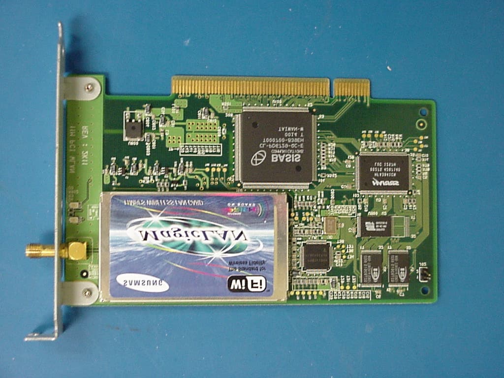
Click to zoom
Application Details
- Equipment Class
- DSS - Part 15 Spread Spectrum Transmitter
- Date of Grant
- Mar 14, 2001
- Application Purpose
- Original Equipment
- Date of Application
- Mar 14, 2001
- Equipment Note
- PCI Card Spread Spectrum Transceiver
- Frequency Range
- 2412.00000000 - 2471.00000000
- Company
- Samsung Electro Mechanics
- Country
- South Korea
Documents & Files
Document Text
Text extracted from the exhibit documents filed with the FCC. Open a document above to read the original.
Users Manual
360 Herndon Parkway Suite 1400 Herndon, VA 20170 http://www.rheintech.com Certification Report For: Samsung Page 39 Document Number: 2000486 21 ANTENNA INSTRUCTION MANUAL INSTALLATION MANUAL Introduction This manual does not substitute your wireless LAN card’s user’s guide. This installation guide must be read for more detailed information about your wireless LAN card’s use, care and maintenance, including important safety information. The Samsung Wireless LAN Card has two antenna connectors for attaching external antennas for coverage area extension. Use only the supplied antenna. Unauthorized antennas, modifications, or attachments could damage the wireless LAN card and may violate regulations governing radio devices. FCC WARNING The SWL-2000E complies with Part 15 of the FCC rules. Operation is subject to the following two conditions; (1) This device may not cause harmful interference. (2) This device must accept any interference received, including interference that may cause undesired operation. RF SAFETY WARNING While installing and operating this transmitter and antenna combination the radio frequency exposure limit of 1mW/cm 2 may be exceeded at distances close to the antennas installed. Therefore, the user must maintain a minimum distance of 20 cm from the antenna. Note: The SWL-2000E has been tested and found to comply with the limits for a Class B digital device and a low power transmitter, according to Part 15 of the FCC Rules. These limits are designed to provide reasonable protection against harmful interference in a residential installation. This equipment generates, uses and can radiate radio frequency energy and, if not installed and used in accordance with the instructions, may cause harmful interference to radio communications. However, there is no guarantee that interference will not occur in a particular installation. If this equipment does cause harmful interference to radio or television reception, which can be determined by turning the equipment off and on, the user is encouraged to resolve the problem by one or more of the following measures; Reorient or relocate the receiving antenna. Increase the separation between the equipment and the receiver. Connect the equipment to an output on a circuit different from that to which the receiver is connected. Consult the dealer or an experienced radio/TV technician for help. INSTALLATION OF THE EXTERNAL ANTENNA The user is responsible for ensuring that the public is not exposed to radio frequency energy levels in excess of the FCC guidelines. Humans cannot be within 20 cm (8 inches) of the front of the antennas. If such a situation occurs, the user is responsible for placing the appropriate caution signs to warn the public. Notebook PC Adapter Card (SWL-2000E) • You can install the card whether the power of the Notebook is on or off. • Insert the SWL-2000E adapter card into the PCMCIA slot. (A pleasant “cheep” sound indicates the regular operation. A low monotonous tone indicates a failure in recognition.). Always maintain a 20cm space between your self, any other person and the antenna. Warning: The antenna should be mounted so that the main beam is not pointing towards areas of heavy human traffic. If you see red Power LED illuminating and green Rx LED is blinking, you are now ready to proceed to software setup. STUB ANTENNA
Attestation Statements
March 12, 2001 American Telecommunications Certification Body, Inc. 6731 Whittier Avenue Suite C110 McLean, VA 22101 To Whom It May Concern: The connector used on the SWL-2100P was a reverse threaded SMA connector. Thank you for your attention to this matter.
Cover Letter(s)
September 22, 2000 American Telecommunications Certification Body, Inc. 6731 Whittier Avenue Suite C110 McLean, VA 22101 To Whom It May Concern: Please be advised that Samsung Electro-Mechanics authorizes Rhein Tech Laboratories, Inc. to act on our behalf, until otherwise notified, for applications submitted to American Telecommunications Certification Body, Inc. (ATCB). We certify that we are not subject to denial of federal benefits, that includes FCC benefits, pursuant to Section 5301 of the Anti-Drug Abuse ACT of 1988, U.S.C. 862. Further, no party, as defined in 47 CFR 1.2002(b), to the application is subject to denial of federal benefits, that includes FCC benefits. Thank you for your attention to this matter.
Cover Letter(s)
Federal Communications Commission Equipment Authorization Branch 7435 Oakland Mills Rd. Columbia, MD 21406 USA Subject: FCC ID: E2XSWL-2100P January 30, 2001 Gentlemen, Samsung Electro-Mechanics hereby requests that the following items be kept confidential under sections 0.457 and 0.459 of the CFR. If this information was to be made public record it would adversely affect the core business. I would like to request the following items be confidential (1) Schematics (2) Block Diagram Sincerely, John Seo Engineering Manager/System Div. ELECTRO-MECHANICS 314,Maetan3-Dong, Paldal-ku,Suwoni, Kyungki-Do,Korea,441-743 TEL82-31-210-5712 FAX82-31-210-5529
Cover Letter(s)
E2XSWL-2100P 1.) It appears the only real change between the "P" and "E" versions of this product are that the "P" version is mounted on a PC card internal to the computer. I am a little mystified as to why there appears to be so much of a discrepancy between the power output of the two versions. Please explain. These devices are familiar but not exactly the same. The PCMCIA card and the PCI card are based on reference design from Harris. The manufacturer Samsung traditionally sets the output power through firm wave internal to both devices. From past experience testing both types of similar products there has always been differences between the two product types. Unfortunately, we have no control over the settings. The output power reported is exactly what it is for both products tested. 2.) RF exposure was calculated using 70 mW EIRP instead of 56mW + 2.15dB [91.8mW EIRP]. Please address. There is a choice of two ways to get the results, the first is to calculate the EIRP based on the conducted power output and the second is to calculate the EIRP based on a radiated emissions measurement. The method used is to calculate the EIRP based on a radiated emissions measurement because it gives a more realistic result to confirm the antenna gain value. The maximum value from both the conducted power output and the radiated emission measurement was used in the calculation. 3.) External Photos missing. The FCC robot wants to se them anyways. Show end view of card and close up of connector and FCC ID. External Photos section 25 has been added to the revised report. 4.) Antenna manual is for PCMCIA version and not this EUT. This section has been removed from the report. 5.) Nmerous incorrect references to PCMCIA version throughout application. See product description for example. Please address. The PCMCIA report was used as the basic report for the PCI. The product description has been corrected and all references to the PCMCIA card has been removed 6.) Need connector attestation. The connector is a reverse threaded SMA Connector. 7.) No RF Exposure warning statements in manual. No proper instructions. Please see the revised manual. 8.) Antenna manual is for wrong equipment [PCMCIA]. Needs better warnings (not mixed with Class B stuff). Installation instructions anyone? Same as 4 and has been removed. 9.) My comments yesterday about the "E" version test report appear to be just as valid. I question if any final check was made to either of these two Samsung filings. To minimize confusion please separate your request for each FCC ID. Thank you I do not have Rachid's email address so I cannot address him directly. I did not have time to review both Applications for the Samsung spread spectrum transmitters, so I just picked one and looked for the most troublesome items. This is an informal review. 1.) The 731 form calls out a power output of .056 watts. RF exposure info calls out an EIRP of 70mW. My calculations shows 56mW with a 2.15dB gain antenna should make ~70mW. Please address. [Rachid Sehb] The measurement that was provided was the output power at the port instead of the EIRP. 2.) Section 2.1 of test report appears to indicate in paragraph 3 that the emission envelope changes with changes in data rate. If so, data must be shown for all data rates throughout report. Statement Removed 3.) Carrier power listed in Section 8 is just 3.8 dBm. This is very far from 25mW. claimed on 731. Rachid Sehb] In Part 15.247 appendix C states the measurement should be performed with a RSW at 100 kHz and VBW>RBW. The reason for this is the low power carrier is due to this configuration. 4.) Section 10 and 14 of test report. It is difficult to understand what has been done with the test methodology as stated. If I assume that a true 1 second per 3 KHz was used, a 17 second sweep would correspond to only ~50 KHz worth of span. Since this is emission is over 11MHz wide, how can I be sure the spectrum analyzer was set to the highest in band emission? Rachid Sehb] Per our phone conversation we agreed that the setup of the test was correct. 5.) Section 11 and 13: Are these Conducted emissions? Please use dBm and not dBuV. There seems to be a mixing of techniques and bandwidth settings when making band edge measurements. Please be sure of your technique. Make annotation bigger. Set center frequency to exact band edge (2400 or 2483.5), and use span with nice neat number. Span and frequency information are missing (except for marker delta). I suspect the 1MHZ/10Hz plots are swept too fast - there appears to be distortion in the trace. Slow down sweep. Rachid Sehb] RTL agrees, that the sweep time was too fast and will be slowed to the appropriate sweep time for future tests. The reason that this measurement was not retaken is in using our engineering judgment we realized that the margin that was resulted made it impossible and improbable that the device would fail with a slower sweep time. 6.) Manual: There is no RF safety info in manual. Correction made 7.) Antenna Manual: The RF safety warning is mixed up with the non-interference issues for Part 15 labeling. Separate and strengthen. This is for the PCMCIA Card and not for this product of the PCI card. 8.) Antenna Manual: Must have better external antenna installation instructions. If RF exposure is dependent on the end user for keeping antenna away from people, then device is not applicable for TCB approval. This comment is for the PCMCIA card and not for this product of the PCI Card. 9.) Internal photographs: Are their two antenna connectors? Can two antennas be hooked up at same time? Is this a diversity setup, or can both antennas be active at same time? This comment is for the PCMCIA Card and not for this product of the PCI Card.
External Photos
360 Herndon Parkway Suite 1400 Herndon, VA 20170 http://www.rheintech.com Certification Report For: Samsung Page 2 Document Number: 2000486 Revision 2 25 EXTERNAL PHOTOGRAPHS Top view
ID Label/Location Info
360 Herndon Parkway Suite 1400 Herndon, VA 20170 http://www.rheintech.com Certification Report For: Samsung Page 41 Document Number: 2000486 23 LABEL INFORMATION 23.1 FCC ID LABEL 23.2 WARNING STATEMENT FCC LABEL AND LOCATION OF LABEL ON EUT Samsung Electro-Mechanics FCC ID: E2XSWL-2100P Canada: XXXXXX This device complies with part 15 of the FCC Rules. Operation is subject to the following two conditions: 1) This device may not cause harmful interference, and 2) this device must accept any interference received, including interference that may cause undesired operation.
Internal Photos
360 Herndon Parkway Suite 1400 Herndon, VA 20170 http://www.rheintech.com Certification Report For: Samsung Page 2 Document Number: 2000486 26 PHOTOGRAPHS Top view 360 Herndon Parkway Suite 1400 Herndon, VA 20170 http://www.rheintech.com Certification Report For: Samsung Page 3 Document Number: 2000486 Top view w/o can 360 Herndon Parkway Suite 1400 Herndon, VA 20170 http://www.rheintech.com Certification Report For: Samsung Page 4 Document Number: 2000486 Bottom view of the board 360 Herndon Parkway Suite 1400 Herndon, VA 20170 http://www.rheintech.com Certification Report For: Samsung Page 5 Document Number: 2000486 Front view 360 Herndon Parkway Suite 1400 Herndon, VA 20170 http://www.rheintech.com Certification Report For: Samsung Page 6 Document Number: 2000486 Antenna
Internal Photos
360 Herndon Parkway Suite 1400 Herndon, VA 20170 http://www.rheintech.com Certification Report For: Samsung Page 3 Document Number: 2000486 Revision 2 26 INTERNAL PHOTOGRAPHS Top view w/o can 360 Herndon Parkway Suite 1400 Herndon, VA 20170 http://www.rheintech.com Certification Report For: Samsung Page 4 Document Number: 2000486 Revision 2 Bottom view of the board 360 Herndon Parkway Suite 1400 Herndon, VA 20170 http://www.rheintech.com Certification Report For: Samsung Page 5 Document Number: 2000486 Revision 2 Front view 360 Herndon Parkway Suite 1400 Herndon, VA 20170 http://www.rheintech.com Certification Report For: Samsung Page 6 Document Number: 2000486 Revision 2 Antenna
Operational Description
360 Herndon Parkway Suite 1400 Herndon, VA 20170 http://www.rheintech.com Certification Report For: Samsung Page 36 Document Number: 2000486 18 PRODUCT DESCRIPTION The model SWL-1105 (referred to as the EUT in this report) is a Direct Sequence Spread Spectrum wireless LAN, PCI network card. The EUT provides wireless communications between computers. The EUT is designed to be installed into the PCI slot of a notebook computer or desktop computer with a PCI slot. The EUT communicates with other wireless LAN cards using the frequency range from 2.412 GHz to 2.471 GHz. The EUT is powered from the PCI slot, and does not have an external power supply. The EUT uses an external antenna. The EUT uses 2-bits encoded to 4 complex code words; 2-DQPSK CCK modulation technique with 8 Chips per symbol, spread clock rate is 1.375 MHz symbol/sec, and the data rate = 11 MBPS.
Test Report
Engineering and Testing for EMC and Safety Compliance 360 Herndon Parkway, Suite 1400 Herndon, VA 20170 Phone: 703-689-0368; Fax: 703-689-2056; Metro: 703-471-6441 APPLICATION FOR FCC CERTIFICATION DIRECT SEQUENCE SPREAD SPECTRUM TRANSMITTER Samsung Electro-Mechanics 314, Maetan-3Dong, Paldal-Gu, Suwon, Kyunggi-Do, Korea, 442-743 +82-331-210-6662 Model: Magic Wave PCI Card SWL-2100P FCC ID: E2XSWL-2100P STANDARDS REFERENCED FOR THIS REPORT PART 2: 1999 FREQUENCY ALLOCATIONS AND RADIO TREATY MATTERS; GENERAL RULES AND REGULATIONS PART 15: 1999 RADIO FREQUENCY DEVICES FCC 97-114 GUIDANCE ON MEASUREMENTS FOR DIRECT SEQUENCE SPREAD SPECTRUM SYSTEMS ANSI C63.4-1992 STANDARD FORMAT MEASUREMENT/TECHNICAL REPORT PERSONAL COMPUTER AND PERIPHERALS RSS-210, Issue 3: 2000 LOW POWER LICENCE-EXEMPT RADIOCOMMUNICATION DEVICES (ALL FREQUENCY BANDS) RSS-102, Issue 1: 1999 EVALUATION PROCEDURE FOR MOBILE AND PORTABLE RADIO TRANSMITTERS FCC Rules Parts Frequency Range Output Power (W) Freq. Tolerance Emission Designator 15.247 2412-2471 MHz 0.056 N/A REPORT PREPARED BY: Test Engineer: Rachid Sehb Technical Writer: Melissa Fleming Supervising Engineer: Desmond A. Fraser Document Number: 2000486 / QRTL00-410 No part of this report may be reproduced without the full written approval of Rhein Tech Laboratories, Inc. 360 Herndon Parkway Suite 1400 Herndon, VA 20170 http://www.rheintech.com Certification Report For: Samsung Page 2 Document Number: 2000486 Revision 3 TABLE OF CONTENTS 1 INTRODUCTION....................................................................................................................................................4 1.1 RELATED SUBMITTAL (S)/GRANT (S).....................................................................................................4 1.2 TEST METHODOLOGY.................................................................................................................................4 1.3 TEST FACILITY...............................................................................................................................................4 1.4 EMISSIONS EQUIPMENT LIST....................................................................................................................5 2 SYSTEM TEST CONFIGURATION...................................................................................................................8 2.1 JUSTIFICATION...............................................................................................................................................8 2.2 EUT EXERCISE SOFTWARE........................................................................................................................8 2.3 SPECIAL ACCESSORIES...............................................................................................................................8 2.4 TEST SYSTEM DETAILS...............................................................................................................................9 2.5 CONFIGURATION OF TESTED SYSTEM................................................................................................10 3 CONFORMANCE STATEMENT......................................................................................................................11 4 FIELD STRENGTH CALCULATION..............................................................................................................12 5 CONDUCTED EMISSIONS MEASUREMENTS............................................................................................13 5.1 CONDUCTED EMISSIONS TEST...............................................................................................................14 5.1.1 Conducted Emissions (Channel 1 With The External Antenna).......................................................15 6 RADIATED EMISSIONS MEASUREMENTS................................................................................................16 6.1 RADIATED EMISSIONS TEST.............................................................................................................................17 6.1.1 Radiated EMISSION DIGITAL noise (Channel 1 with the external Antenna)..............................17 7 MODULATED BANDWIDTH............................................................................................................................18 8 POWER OUTPUT.................................................................................................................................................18 9 ANTENNA CONDUCTED SPURIOUS EMISSIONS.....................................................................................19 10 RADIATED SPURIOUS EMISSIONS...........................................................................................................20 10.1.1 Radiated Emissions Harmonics/spurious (Channel 1).......................................................................20 10.1.2 Radiated Emissions Harmonics/spurious (Channel 6).......................................................................21 10.1.3 Radiated Emissions Harmonics/spurious (Channel 11).....................................................................22 11 POWER SPECTRAL DENSITY.....................................................................................................................23 12 COMPLIANCE WITH THE RESTRICTED BAND EDGE......................................................................23 13 ANTENNA SPECIFICATIONS......................................................................................................................24 14 BANDEDGE PLOTS.........................................................................................................................................25 15 SPECTRAL DENSITY PLOTS.......................................................................................................................29 16 6dB PLOTS.........................................................................................................…
Text truncated - open the document above for the full version.
Test Report
Measurement of Processing Gain of a Direct Sequence Spread Spectrum System Certification Report on Compliance with Respect to FCC CFR 47, Paragraph 15.247(e) Product: Samsung SWL-2100P Wireless LAN Card January 24, 2001 REPORT PREPARED BY: Rick McMurray Rhein Tech Laboratories, Inc. 360 Herndon Parkway, Suite 1400 Herndon, VA 20170 (703) 689-0368 (703) 689-2056 fax Rhein Tech Laboratories, Inc. Scope This report contains the results of the processing gain testing performed on the Samsung SWL- 2100P Wireless LAN Cards. The tests were carried out in accordance with FCC CFR 47, Paragraph 15.247(e). The jamming margin method specified in 15.247(e)(2) was used to perform the processing gain testing. FCC 97-114, Guidance on Measurements for Direct Sequence Spread Spectrum Systems, was also utilized as a guiding document for the performance of the processing gain testing. FCC Requirements The processing gain of a direct sequence system shall be at least 10dB. The processing gain shall be determined from the ratio in dB of the signal-to-noise ratio with the system spreading code turned off to the signal-to-noise ratio with the system spreading code turned on, as measured at the demodulated output of the receiver. Test Equipment Hewlett Packard Spectrum Analyzer, Model 8564E (RTL Asset # 901020) Hewlett Packard Signal Generator, Model 8648C, 100kHz-3200MHz (RTL Asset # 900917) Weinschel Broadband Resistive Power Divider, Model 1515, DC to 18.0GHz 1 Watt Weinschel Directional Coupler, Model 1537RA-20, 0.5 to 4.0GHz IBM ThinkPad Laptop computers used with transmitter and receiver Equipment Under Test Transmitter: Samsung SWL-2000E, MagicLAN Wireless LAN Card Marked #2, R and D sample #10, LEKRDAA05A5C09, Intersil Prism on Board Receiver: Samsung SWL-2000E, MagicLAN Wireless LAN Card Marked #1, R and D sample #11, LEKRDAA05A5C00, Intersil Prism on Board Method of Measurement As mentioned in the scope section, the jamming margin method was used. The following drawing titled “Processing Gain – Jamming Test Setup” illustrates a block diagram of the test setup. In this method, a signal generator was stepped in 50kHz increments across the passband of the system. At each point, the level of the signal generator required to produce the recommended Bit Error Rate (BER) was recorded. This level is the jammer level. The output power of the transmitter was also recorded at these same points. This level is the signal level. The jammer to signal ratio (J/S) was then calculated. The worst 20% of the J/S data points were discarded. The lowest remaining J/S ratio was used to calculate the processing gain for each of the channels investigated. The processing gain, Gp, was calculated as follows: Gp = (S/N)o + Mj + Lsys, where Gp = the processing gain of the system, (S/N)o = signal to noise ratio required Rhein Tech Laboratories, Inc. for the chosen BER, Mj = J/S ratio, and Lsys = system losses. Note that total system losses in a system, including intentional radiator and receiver, are assumed to be no more than 2dB as specified by the FCC. An ideal signal to noise ratio, also referred to as (S/N)o or (Es/No), of 16.4dB was used as specified by Intersil when calculating the processing gain when operating at 11Mbps. The Samsung SWL-2000E contains chip-sets from Intersil and operates at 11Mbps. Please see the enclosed document “Testing for compliance with FCC rules 15-247e” by Carl Andren of Intersil Corporation for more information. The use of 8% FER frame error rate (or PER packet error rate) as a substitute for the recommended BER bit error rate is derived in the attached document “Testing for compliance with FCC rules 15-247e” by Carl Andren of Intersil Corporation. Engineering Summary Processing Gain Results Summary: Channel Rate (Mbps) Gp(dB) 1 11 18.1 6 11 22.1 11 11 19.7 Following are the calculations and data for the three channels that were investigated. THEORETICAL PROCESSING GAIN The table below represents the symbol rate, chip rate, and theoretical processing gain for the aforementioned EUT. Data Rate (Mbps) Symbol Rate (MSps) Chip Rate (MCps) Chip/Symbol Rate Es/No (dB) J/S (dB) 1 1 11 11:1 10.3 -2.3 2 1 11 11:1 13.3 -5.3 5.5 1.375 11 8:1 13.4 -5.4 11 1.375 11 8:1 16.4 -8.4 5 5 4 4 3 3 2 2 1 1 DD CC BB AA Transmitter Samsung SWL-2100P Wireless LAN Card Serial # LEKRDAA05A5C09 Signal Generator HP 8648C RTL Asset # 900917 Broadband Resistive Power Divider Weinschel Model 1515 Spectrum Analyzer HP 8564E RTL Asset # 901020 Receiver Samsung SWL-2100P Wireless LAN Card Serial # LEKRDAA05A5C00 Directional Coupler Weinschel Model 1537A 6dB loss 6dB loss 20dB loss Processing Gain - Jamming Test Setup A 11January 24, 2001 Rhein Tech Laboratories, Inc. Title SizeDocument NumberRev Date:Sheet of Channel 1 Processing Gain 2412MHz 11Mbps After discarding the lowest 20% J/S data points, the lowest J/S was -0.30dB. Gp = (S/N)o + Mj + Lsys = 16.4dB + (-0.30dB) + 2.0dB = 18.1dB 11Mbps Channel 1 Processing Gain Gp = (S/N)o + Mj + Lsys FrequencyGp(S/N)oMj = J/SLsysS (Tx Power)J (S/G Power) (MHz)(dB)(dB)(dB)(dB)(dBm)(dBm) 2407.0023.8016.45.402.0-13.50-8.10 2407.0523.6016.45.202.0-13.50-8.30 2407.1023.6716.45.272.0-13.67-8.40 2407.1523.0316.44.632.0-13.33-8.70 2407.2023.0016.44.602.0-13.50-8.90 2407.2522.2316.43.832.0-12.83-9.00 2407.3022.2716.43.872.0-13.17-9.30 2407.3522.1016.43.702.0-13.00-9.30 2407.4021.6016.43.202.0-12.50-9.30 2407.4522.1016.43.702.0-13.00-9.30 2407.5021.7016.43.302.0-12.50-9.20 2407.5521.8716.43.472.0-12.67-9.20 2407.6021.7716.43.372.0-12.67-9.30 2407.6521.5016.43.102.0-12.50-9.40 2407.7021.4316.43.032.0-12.33-9.30 2407.7521.4316.43.032.0-12.33-9.30 2407.8021.0016.42.602.0-12.00-9.40 2407.8521.3316.42.932.0-12.33-9.40 2407.9020.8716.42.472.0-12.17-9.70 2407.9520.4316.42.032.0-11.83-9.80 2408.0020.0016.41.602.0-11.50-9.90 2408.0520.4016.42.002.0-12.00-10.00 2408.1020.5716.42.172.0-12.17-10.00 2408.1519.8716.41.472.0-11.67-10.20 2408.2019.6016.41.202.0-11.50-10.30 2408.2519.4316.41.032.0-11.33-10.30 2408.30…
Text truncated - open the document above for the full version.
Test Setup Photos
360 Herndon Parkway Suite 1400 Herndon, VA 20170 http://www.rheintech.com Certification Report For: Samsung Page 42 Document Number: 2000486 Revision 2 24 TEST PHOTOGRAPHS 24.1 CONDUCTED MEASUREMENT PHOTOS Front view Rear view 360 Herndon Parkway Suite 1400 Herndon, VA 20170 http://www.rheintech.com Certification Report For: Samsung Page 43 Document Number: 2000486 Revision 2 24.2 RADIATED MEASUREMENT PHOTOS Front view Rear view
Contact Information
Applicant
Jinhwan Lim(Assistant Manager)
Technical Contact
Rhein Tech Laboratories, Inc.Desmond A Fraser
[email protected]703 689 0368
360 Herndon Parkway · Herndon, Virginia · United States
Test Firm
Rhein Tech Laboratories, Inc.Rick McMurray
Technical Specifications
| # | Rule Parts | Frequency Range | Power Output |
|---|---|---|---|
| 1 | 15C | 2.41 GHz - 2.47 GHz | 56.00 mW |
Other Applications from Samsung Electro Mechanics

E2X-ST-GR2900N
Oct 01, 2015ESL Graphic TAG
Equipment Class
DTS - Digital Transmission System
E2X-ST-GM29XXF
Sep 23, 2015ESL Graphic TAG
Equipment Class
DTS - Digital Transmission System
E2X-ST-GM22XXF
Sep 16, 2015ESL Graphic TAG
Equipment Class
DTS - Digital Transmission System
E2X-ST-GM42003N
Sep 10, 2015ESL Graphic TAG
Equipment Class
DTS - Digital Transmission System
E2X-ST-GM6000N
Aug 26, 2015ESL Graphic TAG
Equipment Class
DTS - Digital Transmission System