E2XUCLZD100P0SZIGBEE LIGHTING DIMMER
Samsung Electro Mechanics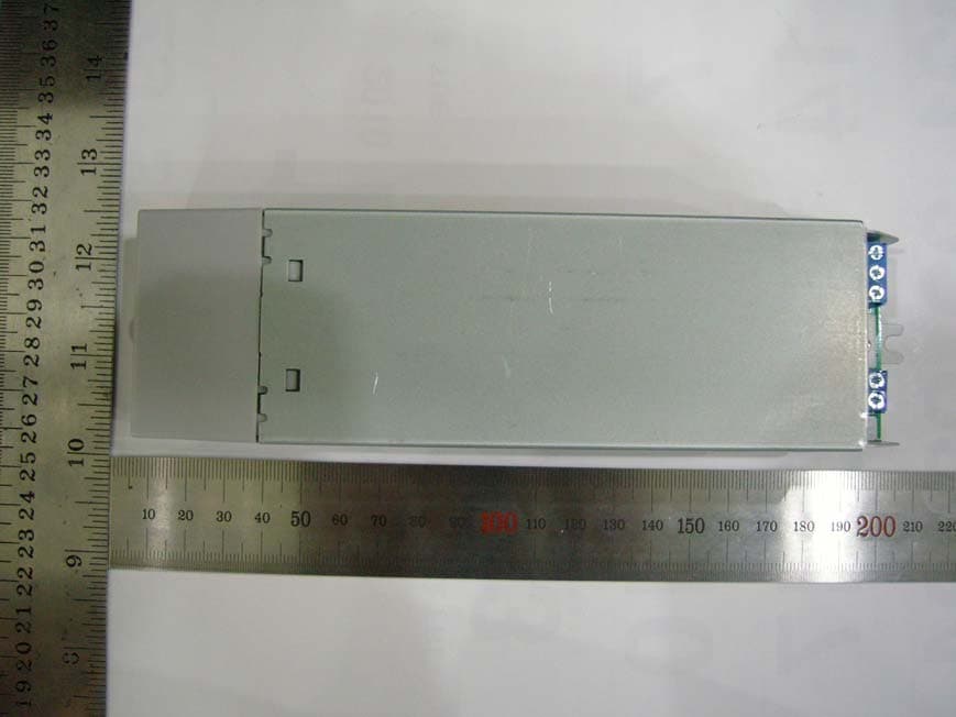
Click to zoom
Application Details
- Equipment Class
- DSS - Part 15 Spread Spectrum Transmitter
- Date of Grant
- May 19, 2010
- Application Purpose
- Original Equipment
- Date of Application
- May 18, 2010
- Equipment Note
- ZIGBEE LIGHTING DIMMER
- Frequency Range
- 2405.00000000 - 2480.00000000
- Company
- Samsung Electro Mechanics
- Country
- South Korea
Documents & Files
Document Text
Text extracted from the exhibit documents filed with the FCC. Open a document above to read the original.
Cover Letter(s)
FCC, Request for non-disclosureDate: May 18, 2010 Page 1 of 1 Samsung Electro Mechanics 314, Maetan3-Dong, Yeongtong-Gu, Suwon, Gyunggi-Do, Korea Subject:Request for confidentiality FCC ID: E2XUCLZD100P0S Reference number: Dear FCC TCB, Persuant to 47 CFR Section 0.459(a) & (b), <name applicant> hereby requests non-disclosure and confidential treatment of the following materials submitted in support of FCC certification application for FCC ID: (E2XUCLZD100P0S) Bill(s) of Material☑ Block Diagrams☑ Operational Description☑ Schematic Diagrams☑ Above materials contain secrets, proprietary and technical information,whichwould customarily be quarded from competitors under 47 CFR, section 0.457(d)(2). Disclosure or publication or any portion of this company confidential material to otherparties could cause substantial competitive harm and provide unjustified benefits for competitors. <Name applicant> understands that pursuant to 47 CFR section 0.457(d)(1)(ii) disclosure of the applicant and all accompanying documentation will not be made before the date of the grant. <Date>May 18, 2010 <City> Suwon <Nameandsignatureofapplicant>
ID Label/Location Info
ID Label Location & Sample 1. Label Location 2. Label Drawing Label position
Internal Photos
Internal view of EUT - Shield Cover mounting state Internal view of EUT - Shield cover Remove state View of Main PCB(Top) - Shield Cover mounting state View of Main PCB(Top) - Shield cover Remove state View of Main PCB(Bottom) - Gab pad mounting state View of Main PCB(Bottom) - Gab pad Remove state
Operational Description
Data sheet of Multilayer Chip Antenna Part No. : ALA131C3 January 23, 2008 AMOTECH Co., LTD. 5B 1L, Namdong Industrial complex, 617 Namchondong, Namdonggu, Incheon, Korea Notes The contents of this data sheet are subject to change without notice. Please confirm the specifications and delivery conditions when placing your order. AMOTECH - 2 - MULTILAYER CHIP ANTENNA Januay 2008 (Rev5.0) 1. SPECIFICATIONS 1.1 Electrical Specifications No ITEM SPEC. Remark 1 Frequency Range 2.4 ~2.485 GHz for ISM 2 VSWR 2.5 : 1 max. 3 Gain Avg. -3 dBi min. 4 Polarization Linear 5 Azimuth Beam Pattern Omni-directional 6 Impedance Nominal 50 Ω ※ These values are measured on the matched reference test board. 1.2 Mechanical Specifications No ITEM SPEC. Remark 1 Internal Electrode Ag Pb-free 2 External Electrode Ag/Ni/Sn Pb-free 3 Dimensions (L x W x H) 11.0 x 3.0 x 1.2 mm 4 Unit Weight 119 ± 9 mg 5 Operating Temperature -35 ~ +85 °C 1.3 Appearance and Dimensions No Name Function Material 1 External Electrode Soldering, Input Port Ag/Ni/Sn 2 Direction index Indication of Input Port Ceramic 4 Ceramic Body - Ceramic 3 Model No. index - Ceramic 5 External Electrode Soldering Ag/Ni/Sn AMOTECH - 3 - MULTILAYER CHIP ANTENNA Januay 2008 (Rev5.0) 2. MEASUREMENT 2.1 Reference Test Board for Measurement Chip Antenna Matching Stage SMA Connector GND [Unit : mm] 2.2 Diagram for VSWR measurement Network Analyzer Styrofoam AUT AMOTECH - 4 - MULTILAYER CHIP ANTENNA Januay 2008 (Rev5.0) 2.3 Diagram for radiation gain and pattern measurements iMac A. Anechoic chamber spec. Parameters Condition Unit Chamber size 8x4x4 m Temperature 21.5 °C Humidity 55 % RH Measurement S21 (8753ES) System software Midas (Orbit/FR) B. Measurement coordinates Measurement Plane Symbol Rotating direction Azimuth Azimuth x→y Elevation1 E1 z→x Elevation2 E2 z →-y x y z -y Azimuth E1 E2 AMOTECH - 5 - MULTILAYER CHIP ANTENNA Januay 2008 (Rev5.0) 3. MEASUREMENT RESULT 3.1 VSWR & Smithchart A. Matching Value (recommend for reference testboard only) ③① ② ① N/C ② 10.0 pF ③ 10.0 nH B. Measured data (for ALA931C5) AMOTECH - 6 - MULTILAYER CHIP ANTENNA Januay 2008 (Rev5.0) 3.2 Radiation Gain and Pattern [Measured data table] Peak Gain (dBi) Average Gain (dBi) Remark Azimuth 2.8 -0.7 @2.45 GHz Elevation1 4.0 -0.3 @2.45 GHz Elevation2 2.6 -1.3 @2.45 GHz [ ALA131C3 radiation pattern : [email protected] ] AMOTECH - 7 - MULTILAYER CHIP ANTENNA Januay 2008 (Rev5.0) [ ALA131C3 radiation pattern : [email protected] ] [ALA131C3 Radiation Pattern : [email protected] ] AMOTECH - 8 - MULTILAYER CHIP ANTENNA Januay 2008 (Rev5.0) 4. SUGGESTED LAYOUT & MATCHING CIRCUIT 4.1 Layout (recommend only) 4.2 Matching Circuit (recommend only) L – type T - type π- type For usable matching, the ground stability must be guaranteed with sufficient via holes and the case effects should be considered. Finally, using one or more lumped chip elements and a tuning stub are recommended for better results. AMOTECH - 9 - MULTILAYER CHIP ANTENNA Januay 2008 (Rev5.0) 5. RELIABILITY TEST No ITEM TEST CONDITION TEST REQUIREMENTS 1 Adhesive Strength of Termination 1. Applied force on SMD chip till detached point from PCB. F SMD PAD PCB 1. No mechanical damage by forces applied on the right. 2. Strength (F) > 7 kgf 2 Tensile Strength 1. Wire : 0.6~0.8 tined Cu wire F Clamp Wire 1. No mechanical damage by forces applied on the right. 2. Strength (F) > 3 kgf 3 Thermal Shock (Temperature Cycle) 1. 1 cycle / step 1 : -40 ± 3°C, 30 min step 2 : +125 ± 3°C, 30 min 2. Number of cycle : 30 3. Measure after left for 48 hrs min. at room temperature 1. No visual damage 2. Within electric spec (VSWR) 4 High Temperature Resistance 1. Temperature : +125 ± 5°C 2. Time : 1000 ± 24 hrs 3. Measure f C after left for 24 hrs min. at room temperature 1. No visual damage 2. Within electric spec (VSWR) 5 Low Temperature Resistance 1. Temperature : -40 ± 5°C 2. Time : 1000 ± 24 hrs 3. Measure f C after left for 48 hrs min. at room temperature 1. No visual damage 2. Within electric spec (VSWR) 6 Humidity (Steady Condition) 1. Humidity : 85 % RH 1. Temperature : +85 ± 3°C 2. Time : 1000 ± 24 hrs 3. Measure f C after left for 48 hrs min. at room temperature 1. No visual damage 2. Within electric spec (VSWR) AMOTECH - 10 - MULTILAYER CHIP ANTENNA Januay 2008 (Rev5.0) 6. SOLDERING RECOMMENDATIOS 6.1 Reflow Soldering Profile [ Soldering Reflow Profile for Pb-free ] 6.2 Soldering Land Pattern AMOTECH - 11 - MULTILAYER CHIP ANTENNA Januay 2008 (Rev5.0) 7. PACKING 7.1 Tape Dimension (unit : mm) A0 3.30±0.10 P0 4.00±0.10 E 1.75±0.10 B0 11.30±0.10 P1 8.00±0.10 F 11.5 K0 1.50±0.10 P2 2.00±0.10 W 24.00±0.30 D0 1.55±0.05 t 0.30±0.05 7.2 Taping Style 7.3 Packing Unit Quantity Size Reel 4,000 ea Φ13” x 24mm Small Box 8,000 ea (2 reel*4,000ea/reel) 350 * 350 * 90 (mm 3 ) Large Box 42,000 ea (3 small box*8,000ea/small box) 390 * 390 * 280 (mm 3 ) AMOTECH - 12 - MULTILAYER CHIP ANTENNA Januay 2008 (Rev5.0) 7.4 Description of Packing Label AMOTECH CO., LTD. Name of Company 617 5B 1LT, Namchon-Dong, Namdong-Gu, Inchon, Korea Address of Manufacture Multilayer Chip Antenna Name of Component Type : ALA131C3 Lot No : MA13A3060501 Quantity : 4,000 pcs Quantity : 4,000 pcs Date : 2006/05/24 Date : 2006 /05 /24 8. STORAGE CONDITION A. Storage environment must be at an ambient temperature of 15~35°C and an ambient humidity of 45~75 % RH. (MSL Level 2) B. Chip antenna can experience degradation of termination solderability when subjected to high temperature of humidity, or if exposed to sulfur or chlorine gases. C. Avoid mechanical shock (ex. falling) to the chip antenna to prevent mechanical cracking inside of the ceramic dielectric due to its own weight. ALA : Amotech LTCC Antenna 131 : Chip Size C3 : Version & Frequency index MA : Mass-product Antenna 13 : Chip Size A3 : Version & Frequency index 0605 : Date (year/month) 01 : Order of production
Parts List/Tune Up Info
Operational Description This product is a wireless ZLD(ZigBee Lighting Dimmer) device. The ICPZBM-240 is a single module RF transceiver that operates in the world wide 2.4 GHz ISM band. The module consist of RF Transceiver, RF circuitry and 8051-compatible MCU offering ZigBee network protocol and 802.15.4 MAC protocol. The IEEE 802.15.4 based wireless module is using ICPZBM-240 chipset. The ICPZBM-240 can be utilized in systems used in conjunction with simple microcontroller that only need to handle low speed tasks over the serial ports. They will be transmitted from ANT through the Filter to receiver. The RF signal from transmitter is received via ANT. And they go through Filter into the ICPZBM-240.
Test Report
Report Number : KSQ-FCC100407FCC ID : E2XUCLZD100P0S Page 2 /34 TABLE OF CONTENTS 1. GENERAL.................................................................................................................................................4 2. TEST SITE.................................................................................................................................................4 2.1 Location................................................................................................................................................4 2.2 Test Date...............................................................................................................................................4 2.3 Test Environment..................................................................................................................................4 3. DESCRIPTION OF THE EQUIPMENT UNDER TEST..........................................................................5 3.1 Rating and Physical Characteristics.......................................................................................................5 3.2 Equipment Modifications......................................................................................................................5 3.3 Submitted Documents...........................................................................................................................5 4. MEASUREMENT CONDITIONS............................................................................................................6 4.1 Description of test configuration...........................................................................................................6 4.2 List of Peripherals.................................................................................................................................6 4.3 Type of Used Cables..............................................................................................................................6 5. TEST AND MEASUREMENT.................................................................................................................7 5.1 ANTENNA REQUIREMENT..............................................................................................................7 5.1.1 Regulation.......................................................................................................................................7 5.1.2 Result..............................................................................................................................................7 5.2. 6dB BANDWIDTH.............................................................................................................................8 5.2.1 Regulation.......................................................................................................................................8 5.2.2 Test Condition................................................................................................................................8 5.2.3 Test result........................................................................................................................................8 Table 1 : Measured values of the 6dB Bandwidth...........................................................................................8 Figure 1 Plot of the 6dB Channel Bandwidth................................................................................................9 5.3. MAXIMUM PEAK POWER...........................................................................................................11 5.3.1 Regulation.....................................................................................................................................11 5.3.2 Test Condition...............................................................................................................................11 5.3.3 Test result......................................................................................................................................11 Table 2 : Measured values of the Maximum Peak Output Power(Conducted)......................................................11 Figure 2 : Plot of the Maximum Peak Output Power(Conducted).....................................................................12 5.4. PEAK POWER SPECTRAL DENSITY............................................................................................14 5.4.1 Regulation.....................................................................................................................................14 5.4.2 Test Condition...............................................................................................................................14 Report Number : KSQ-FCC100407FCC ID : E2XUCLZD100P0S Page 3 /34 5.4.3. Test result.....................................................................................................................................14 Table 3 : Measured values of the Peak Power Spectral Density........................................................................14 Figure 3 : Plot of the Peak Power Spectral Density........................................................................................15 5.5. SPURIOUS EMISSIONS, BAND EDGE, AND RESTRICTED BANDS........................................17 5.5.1 Regulation.....................................................................................................................................17 5.5.2 Test Setup Layout..........................................................................................................................18 5.5.2.1 Radiated Emission Test Set-Up, Frequency Below 1000MHz.................................................18 5.5.2.2 Radiated Emission Test Set-UP Frequency Over 1000MHz ....................................................18 5.5.3 Test Procedure.............................................................................................................…
Text truncated - open the document above for the full version.
Contact Information
Applicant
Jinhwan Lim(Assistant Manager)
Test Firm
Korea Standard Quality LaboratoriesSung-goo Kim
Technical Specifications
| # | Rule Parts | Frequency Range | Power Output |
|---|---|---|---|
| 1 | 15C | 2.40 GHz - 2.48 GHz | 500.00 µW |
Other Applications from Samsung Electro Mechanics

E2X-ST-GR2900N
Oct 01, 2015ESL Graphic TAG
Equipment Class
DTS - Digital Transmission System
E2X-ST-GM29XXF
Sep 23, 2015ESL Graphic TAG
Equipment Class
DTS - Digital Transmission System
E2X-ST-GM22XXF
Sep 16, 2015ESL Graphic TAG
Equipment Class
DTS - Digital Transmission System
E2X-ST-GM42003N
Sep 10, 2015ESL Graphic TAG
Equipment Class
DTS - Digital Transmission System
E2X-ST-GM6000N
Aug 26, 2015ESL Graphic TAG
Equipment Class
DTS - Digital Transmission System