GAFFR22-NL22 Channels 2 Way Radio
Columbia Telecommunications Group Inc
Click to zoom
Application Details
- Equipment Class
- FRF - Part 95 Family Radio Face Held Transmitter
- Date of Grant
- Jan 29, 2004
- Application Purpose
- Original Equipment
- Date of Application
- Jan 29, 2004
- Equipment Note
- 22 Channels 2 Way Radio
- Frequency Range
- 462.55000000 - 462.72500000
- Country
- United States
Documents & Files
Document Text
Text extracted from the exhibit documents filed with the FCC. Open a document above to read the original.
Users Manual
COLUMBIA OPERATIONS MANUAL FRS22-NL General Mobile Radio Service (GMRS) 22 Channel 2-Way Radios GMRS/FRS Frequencies Voice-Activated Earpiece Included Owners Manual and Instructions 2 Contents.................................................................................2 Introduction.................................................................. 6 Controls and Displays............................................ 6 Component Guide........................................................ 7 Setting Up Your GMRS/FRS Radio ............................... 8 Battery Installation .................................................. 8 Battery Meter ........................................................... 9 Low Battery Indicator ............................................... 9 Operation .................................................................... 11 Turning on your GMRS/FRS .................................. 11 Communication..................................................... 11 Receiving communications................................... 11 Respond prompt tone.......................................... 12 Channel selection................................................ 12 Frequencies.......................................................... 13 To speak to another radio ..................................... 14 Range................................................................... 14 Calling (Paging) another radio ............................. 15 Setting Call-Ring Tone................................................15 Key Tone ON/OFF.........................................................16 Roger Beep ON/OFF....................................................16 Dual Channel Monitor..................................................17 To set the time..............................................................18 To set alarm clock........................................................18 Using stopwatch..........................................................19 Special Features ........................................................ 20 Automatic Squelch ................................................ 20 Channel Lock................................................................20 Channel Scan ....................................................... 20 Automatic Battery Save ......................................... 21 External Microphone/Speaker/Charger Jacks ...... 21 Built-in flashlight...........................................................21 Customer Support ..................................................... 22 Channel Frequencies and Code Charts ................... 23 Warranty .................................................................... 24 Contents CAUTION.................................................................................3 SAFETY TRAINING INFORMATION....................................4 FCC Warning..........................................................................5 3 GMRS LICENSE USE OF THIS RADIO WITHIN THE UNITED STATES REQUIRES AN FCC GMRS LICENSE. AN INDIVIDUAL 18 YEARS OF AGE OR OLDER, WHO IS NOT A REPRESENTATIVE OF A FOREIGN GOVERNMENT, IS ELIGIBLE TO APPLY FOR A GMRS SYSTEM LICENSE. YOU WILL NEED TWO FORMS FROM THE FCC; FCC FORM 159 AND FCC FORM 605 MAIN FORM AND SCHEDULE F. YOU CAN FIND THE FORMS ONLINE AT:HTTP// WWW.FCC.GOV/FORMPAGE.HTWL ,OR CALL 1-800- 418-3676. To maintain compliance with the FCC`s RF exposure guidelines, hold the transmitter at least 1 inch (2.5 centimeters) from your face and speak in a normal voice, with the antenna pointed up and away. If you wear the handset on your body while using the headset accessory, DO NOT TRANSMIT. The FRS-22 supplied belt clip is for storage purposes ONLY. Use only the supplied antenna. Unauthorized antennas, modifications, or attachments could damage the transmitter and may violate FCC regulations. Normal Position :Hold the transmitter approximately 1” from your face and speak in a normal voice, with the antenna pointed up. MODIFICATIONS OR CHANGES NOT EXPRESSLY APPROVED BY COLUMBIA TELECOMMUNICATIONS, INC. COULD VOID THE USER`S AUTHORITY TO OPERATE THE EQUIPMENT. CAUTION 4 Safety Information For GMRS UNIT Your wireless handheld portable transceiver contains a low power transmitter. When the TALK button is pushed it sends out radio frequency (RF) signals . This device is authorized to operate at a duty factor not to exceed 50% In August 1996,the Federal Communications Commission (FCC) adopted RF exposure guidelines with safety levels for handheld wireless devices. . DO NOT operate the radio without a proper antenna attached , as this may damage the radio and also cause you to exceed FCC RF exposure limits . A proper antenna is the antenna supplied with this radio by the manufacturer or an antenna specifically authorized by the manufacturer for use with this radio. . DO NOT transmit for more than 50% of total radio use time (50% duty cycle) Transmitting more than 50% of the time can cause FCC RF exposure compliance requirements to be exceeded. .ALWAYS use authorized accessories antennas, batteries,belt clips, speaker/mic, etc). Use of unauthorized accessories can cause the FCC RF exposure compliance requirements to be exceeded. ALWAYS keep the antenna at least 2.5cm (1 inch) away from the body when transmitting ,If you wear the handset on your body while using the headset accessory, DO NOT TRANSMIT. The FRS-22 supplied belt clip is for storage purposes ONLY. This is to ensure FCC RF exposure compliance requirements are not exceeded. To provide the recipients of your transmission the best sound quality, hold the antenna at least 5cm(2 inches) from the mouth, and slightly off to one side. SAFETY TRAINING INFORMATION 5 ADJUSTMENT: REPLACEMENT or substitution of transistors, regular diodes or other parts of a unique nature, with parts other than those recommended by Columbia, may cause a violation of the technical regulations of part 95 of the FCC Rules, or violation of Type Acceptance …
Text truncated - open the document above for the full version.
External Photos
APPENDIX C - EUT EXTERNAL PHOTOGRAPHS Chassis - Front View Chassis – Rear View
ID Label/Location Info
APPENDIX A - FCC ID LABELING AND LOCATION Proposed FCC ID Labeling Specifications: Text is black or white in color and is left justified. Labels are silk-screened and shall be “permanently affixed” at a conspicuous location on the EUT. Proposed FCC ID Location Rear Side of EUT / Proposed Label Location Labeling Requirement Each equipment for which a type acceptance applications is filed on or after May 1, 1981, shall bear an identification plate or label pursuant to §2.295 (Identification of Equipment) and §2.926 (FCC identifier) In August 1996 the Federal Communications Commissions (FCC) adopted RF exposure guidelines with safety levels for hand-held wireless devices. Generally users manual contains a RF exposure statement to indicate compliance with FCC requirements. The users manual should also contain required information and instruction pursuant to 95.653. FCC ID: GAFFRS22-NL FCC ID: GAFFRS22-NL
Internal Photos
APPENDIX C - EUT INTERNAL PHOTOGRAPHS EUT - Uncovered View EUT - Component View without Shielding EUT - Component View with Shielding EUT – Solder View EUT – Antenna Connection View
Operational Description
- 1 - CIRCUIT DESCRIPTION 1. RECEIVER SECTION Radio Frequency signal received by the antenna (ANT1), passing through the Low Pass Filter (L1,L3, C2-C5). The RF signal is then amplified by Low Noise Amplifier Q1 and passes through a Band Pass Filter of C96 C122 L7. The filtered signal within the range of 462 MHz – 467 MHz is then mixed with the first local oscillator signal from the Voltage Controlled Oscillator (VCO) circuit (Q11,Q10, D7, L18) through Q3, a portion of VCO signal is then feedback to the PLL IC (IC2) for phase comparison generating a stable RX frequency, the output signal is filtered by FL2 (21.7 MHz) which is the first Intermediate Frequency (IF) and is then amplified by Q4. The IF signal is fed to the discriminator IC1 pin 16 which is then mixed with the second local oscillator supplied by crystal X1 (21.25 MHz) to produced a reduced second IF signal which is then filtered by FL3 (LTM450HTU). Demodulated signal is recovered through correct and the internal discriminator circuit of IC1. The recovered Audio signal is outputted at pin 9 of IC1 and then processed through filtering done by pin#18,19 of IC4, the fully recovered audio signal is then further amplified by Power Amplifier IC5. An audible sound is therefore produce by the speaker SPK1, which can be varied digitally from the CPU pins 28,29,30 and the corresponding series of resistors R4,R16,R66. 2. TRANSMITTER SECTION PTT switch (SW7) when pushed triggers the Transmitter Circuit “ON”, the voice signal generates by the surrounding noise passes through the microphone MIC1 where mechanical to electrical transformation occurs, the electrical transformed signal is then filtered by Q18. The output signal is Modulated by a modulator circuit with a varactor diode D7 and L18. The external components from Q10,Q11 form a VCO Circuit which generates the required oscillating frequency for transmission, a portion of this signal is feedback to the PLL IC2 pin 14 for phase comparison in order to produce a stabilized TX frequency. The modulated signal is then amplified by a Cascaded Amplifier Circuit Q7 and Q8 and again amplified by Q6 to produce a sufficient Radio Frequency signal emitted by the Antenna (ANT1). 3. CALL TRANSMISSION By pushing the CALL key, a signal is detected by the CPU (IC4), a CALL data is then produced by the CPU. This data passes through the Low Pass Filter Q18 and modulated by the varactor diode D7 and L18. The signal follows it’s conventional transmission section path through the antenna. - 2 - 4. BATTERY LOW DETECTION Battery Low Detection is controlled by the CPU pin 36 as detected on the LCD 1, however a voltage divider circuit R52,60 and R65 serve as the stabilize reference voltage for the CPU to process its detection. 5. SQUELCH DETECTION Supported by the linear IC circuit (IC1), a resistor R21 sets the level of detection and Diode D3 acts as a comparator circuit interface with the CPU. 6. POWER SUPPLY Supply voltage of 3.6 Volts dc is needed to power “ON” the whole circuitry, by Lithium Ion Rechargeable battery pack. 7. Battery Charging Battery Charging by DC adaptor through the ear jack and CPU pin36 monitoring the charging status and once its fully charged the Q17 turn off to stop the charge to protect battery from its over charge. FREQUENCY CHART CHANNEL FREQUENCY (MHz) CHANNEL FREQUENCY (MHz) 1 462.5625 12 467.6625 2 462.5875 13 467.6875 3 462.6125 14 467.7125 4 462.6375 15 462.5500 5 462.6625 16 462.5750 6 462.6875 17 462.6000 7 462.7125 18 462.6250 8 467.5625 19 462.6500 9 467.5875 20 462.6750 10 467.6125 21 462.7000 11 467.6375 22 462.7250
Parts List/Tune Up Info
BILL OF MATERIALMODE:FRS14-NL Rev.00 24-Nov-03 NO PART NAME DESCRIPTION Q'TY REFERENCE A NU./VEND O U/PAMOUNT 1 (0402)COG 22P CHIP CAP_22P 4 C108 109 113 117 2 (0402)X7R 152K CHIP CAP_B_1N 2 C7 74 3 (0402)X7R 103K CHIP CAP_10N 2 C3 401 4 (0402)Y5V 104M CHIP CAP_100N 3 C55 60 97 5 (0603)C0G 010B CHIP CAP_1P 1 C120 6 (0603)C0G 020B CHIP CAP_2P 1 C22 7 (0603)C0G 030B CHIP CAP_3P 1 C16 8 (0603)C0G 3P3B CHIP CAP_3P3 2 C58 63 9 (0603)C0G 040B CHIP CAP_4P 1 C64 10 (0603)C0G 050B CHIP CAP_5P 2 C36 56 11 (0603)C0G 5P6B CHIP CAP_5P6 1 C122 12 (0603)C0G 060D CHIP CAP_6P 1 C39 13 (0603)C0G 070D CHIP CAP_7P 3 C35 44 67 14 (0603)C0G 080D CHIP CAP_8P 1 C66 15 (0603)C0G 090D CHIP CAP_9P 1 C13 16 (0603)C0G 100D CHIP CAP_10P 9 C2 8 40 42 61 62 89 96 312 17 (0603)C0G 120J CHIP CAP_12P 1 C5 18 (0603)C0G 180J CHIP CAP_18P 1 C4 19 (0603)C0G 220J CHIP CAP_22P 5 C14 20 27 51 76 20 (0603)C0G 680J CHIP CAP_68P 1 C50 21 (0603)C0G 820J CHIP CAP_82P 1 C111 22 (0603)C0G 101J CHIP CAP_100P 5 C37 49 98 99 149 23 (0603)C0G 221J CHIP CAP_220P 1 C87 24 (0603)X7R 471K CHIP CAP_B_470P 7 C1 10 12 31 32 41 43 25 (0603)X7R 102K CHIP CAP_B_1N 13 C21 28 33 68 71 85 86 90 94 95 123 205 502 26 (0603)X7R 103K CHIP CAP_B_10N 8 C15 72 77 79 80 81 121 301 27 (0603)X7R 223K CHIP CAP_B_22N 1 C88 28 (0603)X7R 333M CHIP CAP_B_33N 1 C17 29 (0603)Y5V 473M CHIP CAP_F_47N 5 C34 45 59 105 106 30 (0603)Y5V 104M CHIP CAP_F_100N 20 C6 18 19 23 25 26 30 38 46 53 54 69 70 78 82 100 104 302 305 311 31 (0603)Y5V 105Z CHIP CAP_F_1000N 8 C11 29 47 57 75 112 118 140 32 (0603)5.6NJ CHIP COIL_5.6NH 1 L10 33 (0603)10NJ CHIP COIL_10NH 1 L5 34 (0603)15NJ CHIP COIL_15NH 1 L202 35 (0603)22NJ CHIP COIL_22NH 5 L2 6 11 13 14 36 (0603)33NJ CHIP COIL_33NH 1 L15 37 (0603)27NJ CHIP COIL_27NH 2 L7 16 38 (0603)68NJ CHIP COIL_68NH 1 L12 39 (0603)2R2K CHIP COIL_2.2uH 1 L8 40 (0402)-10 000J CHIP RES-0 OHM 1 R74 41 (0402)-10 220J CHIP RES-22 OHM 1 R59 42 (0402)-10 152J CHIP RES-1K5 OHM 1 R16 43 (0402)-10 302J CHIP RES-3K OHM 1 R4 44 (0402)-10 682J CHIP RES-6K8 OHM 1 R66 45 (0402)-10 103J CHIP RES-10K OHM 4 R17 54 37 82 46 (0402)-10 683J CHIP RES-68K OHM 1 R49 47 (0402)-10 104J CHIP RES-100K OHM 1 R77 48 (0402)-10 474J CHIP RES-470K OHM 1 R69 49 (0603)-10 100J CHIP RES-10 OHM 4 R14 42 93 508 50 (0603)-10 330J CHIP RES-33 OHM 4 R20 48 51 95 51 (0603)-10 390J CHIP RES-39 OHM 2 R7 R8 52 (0603)-10 560J CHIP RES-56 OHM 3 R41 62 168 53 (0603)-10 101J CHIP RES-100 OHM 2 R3 5 54 (0603)-10 121J CHIP RES-120 OHM 1 R507 55 (0603)-10 561J CHIP RES-560 OHM 1 R167 56 (0603)-10 102J CHIP RES-1K OHM 3 R38 49 40 57 (0603)-10 152J CHIP RES-1K5 OHM 1 R52 58 (0603)-10 182J CHIP RES-1K8 OHM 2 R11 23 59 (0603)-10 222J CHIP RES-2K2 OHM 6 R27 45 46 56 58 89 60 (0603)-10 332J CHIP RES-3K3 OHM 3 R10 13 28 61 (0603)-10 392J CHIP RES-3K9 OHM 3 R15 91 92 62 (0603)-10 472J CHIP RES-4K7 OHM 10 R30 31 43 50 61 73 81 87 146 506 63 (0603)-10 562J CHIP RES-5K6 OHM 2 R33 78 64 (0603)-10 682J CHIP RES-6K8 OHM 2 R25 102 65 (0603)-10 103J CHIP RES-10K OHM 9 R9 26 47 70 79 90 94 139 140 66 (0603)-10 123J CHIP RES-12K OHM 3 R21 34 44 67 (0603)-10 153J CHIP RES-15K OHM 1 R84 68 (0603)-10 183J CHIP RES-18K OHM 1 R1 69 (0603)-10 223J CHIP RES-22K OHM 2 R29 67 70 (0603)-10 303J CHIP RES-30K OHM 1 R60 71 (0603)-10 473J CHIP RES-47K OHM 8 R12 18 71 76 86 88 505 509 72 (0603)-10 683J CHIP RES-68K OHM 2 R63 137 73 (0603)-10 753J CHIP RES-75K OHM 1 R105 74 (0603)-10 823J CHIP RES-82K OHM 2 R2 19 75 (0603)-10 104J CHIP RES-100K OHM 5 R53 57 64 65 68 77 (0603)-10 334J CHIP RES-330K OHM 1 R22 78 (0603)-10 564J CHIP RES-560K OHM 1 R55 79 (0603)-10 684J CHIP RES-680K OHM 1 R6 80 (0603)-10 105J CHIP RES-1M OHM 1 R24 81 1N4148 SWITCHING-DIODE 6 D2 3 5 6 9 11 82 8.2V/0.5W DIODE-ZEN BZ55-8V2 1 DZ1 83 2SC4901 RF-T.R 2SC4901 6 Q1 3 7 8 10 11 84 2SC5343 RF-T.R 3 Q13 18 21 85 2SC5345 RF-T.R 1 Q4 86 2SK3078 RF POWER_T.R(SOT-89) 1 Q6 87 0.32-1.2-3T SPRING CHIP COIL 3 L1 3 9 88 0.32-1.2-4T SPRING CHIP COIL 2 L4 18 89 KT9753-62-2P C-MIC 1 MIC 90 KB8825B PLL_IC_SOP 1 IC2 91 MC34119 AUDIO AMP_IC_SOP 1 IC5 92 KA3361D IF DEMODEULATOR_IC_SOP 1 IC1 93 ITC-SIB302K25FWM2A CPU-PELLET-OTP 1 IC4 94 S-L2980A33MC-C6STF REGULATOR_IC_3.3V 1 IC3 95 HVU202A VARICAP-DIODE 1 D7 96 SRC1203SFY SW-T.R 1 Q16 97 2SA1981SFY SW_T.R 2 Q14 22 98 STN2907SFY SW_T.R 3 Q2 5 12 99 10/10V_TANTAL ELEC_CAP_10UF/10V 1 C73 100 100/6V3_MINI(4X7) ELEC_CAP_100UF/6.3V(4X7) 5 C24 48 101 103 114 101 HC-49S21.250MHZ XTAL 18pF-21.25M+/-2.5PPM 1 X1 102 CERAMIC3.58MHZ CERAMIC RESONATOR 1 X4 103 CDB450C32 CERAMIC DISCRIMINATOR 1 IFT1 104 KTM450HTU CERAMIC FILTER 450+/-3KHz 1 FL3 105 FILTER UM-5 21.7MHZ XTAL FILTER 21.7MHZ +/-3.75 1 FL2 106 32.768KHZ XTAL 1 X5 107 KDS114 RF-SWITCHING-DIODE 3 D1 4 8 108 FLASH LED LED-BLUE 1 LED3 109 LTST-C150GKT CHIP LED GREEN 3 LED1 LED2 LED4 110 SHEET COPPER 10X8X0.1MM 1 111 ECRLA006A52 TRIM_CAP-6P-6PIE 1 CV1 112 16OHM 0.5W 28MM SPEAKER 16OHM 0.5W 28MM SPEAKER 1 SPK1 113 ST-020SMT-050-10 PHONE JACK 1 JACK1 114 PWI8260TW NACKLACE/LCD 1 LCD1 115 ANT NACKLACE/465MHZ NACKLACE 1 ANT1 116 LCD BRACKET NACKLACE 1 117 LCD HOLDER NACKLACE 1 118 NACKLACE-PCB-00 4LAYER 1 119 VCO CAN NACKLACE
Parts List/Tune Up Info
ALIGNMENT PROCEDURE AND SPECIFICATION A. STANDARD TEST CONDITION 1. RF IN/OUT IMPEDANCE ----- 50 OHM 2. RF SIGNAL GENERATOR RF OUTPUT ----- -47dBm MODULATION ----- 1 Khz, 0.5 Khz DEVIATION 3. SPEAKER OUTPUT IMPEDANCE ----- 16 OHM 4. SPEAKER VOLUME ----- MAXIMUM 5. MIC INPUT SIGNAL ----- 1 Khz 10 mVrms 6. POWER SUPPLY ----- DC4.5V +/- 15 % 7.POWER SUPPLY RF AMP -----VOLTAGE:4.5V/CURRENT:350mA B. ELECTRICAL TEST ITEMS 1. VCO VOLTAGE ADJUSTMENT 1) PRESS AND HOLD DOWN THE POWER BUTTON TO POWER ON 2) PRESS THE PTT BUTTON INTO THE TX MODE 3) CONNECT THE DC VOLT METER TO TP1 4) ADJUST L18 AND OBSERVE DC VOLTAGE LIMIT : 0.8 +/- 0.3 Vdc 2. FREQUENCY ADJUSTMENT 1) CONNECT THE FREQUENCY COUNTER TO ANT POINT 2) PRESS THE PTT BUTTON 3) ADJUST THE FREQUENCY BY CV1 LIMIT : +/- 100 Hz 3. TX POWER CHECK 1) CONNECT THE RF POWER METER TO ANT POINT 2) PRESS THE PTT BUTTON 3) MEASURE THE TX POWER LIMIT : 26 dBm +/- 1 dB 4. MIC MODULATION SENSITIVITY CHECK 1) CONNECT THE MODULATION METER TO ANT. 2) THE AUDIO SIGNAL INPUT TO MIC. 3) PRESS THE PTT BUTTON 4) MEASURE THE MODULATE DEV. LIMIT : 0.9 +/- 0.3 Khz DEV . 5. MAXIMUM DEVIATION CHECK 1) CONNECT THE MODULATION METER TO ANT. 2) THE AUDIO SIGNAL INPUT TO MIC. 3) INCREASE THE AUDIO LEVEL BY 20DB 4) PRESS THE PTT BUTTON 5) MEASURE THE MODULATE DEV. LIMIT : 1.9 +/- 0.4 Khz DEV . 6. CALL SIGNAL MODULATION DEV. CHECK 1) CONNECT THE MODULATION METER TO ANT. 2) PRESS THE CALL BUTTON 3) MEASURE MODULATE DEV. LIMIT : 1.2 +/- 0.3 Khz DEV. 7. LOW BATTERY DETECT CHECK 1) VARY THE DC POWER 2) OBSERVE THE BATTERY ICON INSIDE BARS DISAPPEARED 3) MEASURE THE DC POWER VOLTAGE LIMIT : 3.5 +/- 0.1 Vdc 8. ESCRIMINATOR ADJUST 1) CONNECT THE SSG TO ANT. 2) CONNECT THE DC VOLT METER TO TP10 3) ADJUST IFT1 AND MEASURE TP10 VOLTAGE LIMIT : 1.3 +/- 0.2 Vdc 9. SPEAKER OUTPUT LEVEL CHECK 1) CONNECT THE SSG TO ANT. 2) CONNECT THE AUDIO VOLT METER TO SPK. 3) MEASURE THE SPEAKER OUTPUT LEVEL LIMIT : -1 +/- 4 dBm 10. RECEIVING SENSITIVITY CHECK 1) CONNECT THE SSG TO ANT. 2) CONNECT THE SINAD METER TO SPK. 3) REDUCE THE SSG RF OUT PUT LEVEL UP TO SINAD 12dB 4) MEASURE THE SSG RF OUTPUT LEVEL LIMIT : < -116 dBm 11. SQ CHECK 1) CONNECT THE SSG TO ANT. 2) CONNECT THE SINAD METER TO SPK. 3) CONNECT THE DC VOLT METER TO TP12 4) REDUCE THE SSG RF OUTPUT UP TO TP12 IS CHATERING 5) MEASURE THE SINAD METER LIMIT : 6 +/- 2 dB
Schematics
Nefrs.sch-1 - Tue Nov 25 17:49:23 2003
Test Report
Note: This test report is specially limited to the above client company and product model. It may not be duplicated without prior written consent of Bay Area Compliance Laboratory Corporation. This report must not be used by the client to claim product endorsement by NVLAP or any agency of the U.S. Government. FCC PART 95 EMI MEASUREMENT AND TEST REPORT For Columbia Telecommunications Group Inc. 174 Milbar Blvd. Farmingdale, NY 11735 FCC ID: GAFFRS22-NL 2004-01-29 This Report Concerns: Original Report Equipment Type: 22 Channel 2-Way Radio Test Engineer: Ling Zhang / Report Number: R0312013 Test Date: 2003-12-01 Reviewed By: Ming Jing / Prepared By: Bay Area Compliance Laboratory Corporation 230 Commercial Street Sunnyvale, CA 94085 Tel: (408) 732-9162 Fax: (408) 732 9164 Columbia Telecommunications Group Inc. FCC ID: GAFFRS22-NL Report # R0312013Rpt.doc FCC Part 95 Test Report Page 2 of 23 TABLE OF CONTENTS GENERAL INFORMATION.......................................................................................................................................4 PRODUCT DESCRIPTION FOR EQUIPMENT UNDER TEST (EUT) ....................................................................................4 OBJECTIVE...................................................................................................................................................................4 RELATED GRANT/SUBMISSION.....................................................................................................................................4 TEST METHODOLOGY..................................................................................................................................................4 TEST FACILITY.............................................................................................................................................................4 SYSTEM TEST CONFIGURATION ..........................................................................................................................6 JUSTIFICATION.............................................................................................................................................................6 EUT TEST CONFIGURATION........................................................................................................................................6 SPECIAL ACCESSORIES.................................................................................................................................................6 SCHEMATICS / BLOCK DIAGRAM.................................................................................................................................6 EQUIPMENT MODIFICATIONS.......................................................................................................................................6 CONFIGURATION OF TEST SYSTEM..............................................................................................................................6 TEST SETUP BLOCK DIAGRAM.....................................................................................................................................7 REQUIREMENTS OF PROVISIONS ........................................................................................................................8 TEST SUMMARY...........................................................................................................................................................8 §2.1046, §95.639(D), AND §95.639 (A)(1) - EFFECTIVE RADIATED POWER ....................................................9 STANDARD APPLICABLE..............................................................................................................................................9 TEST PROCEDURE........................................................................................................................................................9 TEST EQUIPMENT.......................................................................................................................................................10 ENVIRONMENTAL CONDITIONS..................................................................................................................................10 TEST RESULTS...........................................................................................................................................................10 §2.1047, §95.631(D), §95.637(A), AND § 95.637(B) - MODULATION CHARACTERISTICS ...........................11 STANDARD APPLICABLE............................................................................................................................................11 TEST PROCEDURE......................................................................................................................................................11 TEST EQUIPMENT.......................................................................................................................................................11 ENVIRONMENTAL CONDITIONS..................................................................................................................................12 TEST RESULTS...........................................................................................................................................................12 §2.1049, §95.633(A), AND § 95.633(C) - OCCUPIED BANDWIDTH OF EMISSION.........................................14 STANDARD APPLICABLE............................................................................................................................................14 TEST PROCEDURE......................................................................................................................................................14 TEST EQUIPMENT.......................................................................................................................................................14 ENVIRONMENTAL CONDITIONS.....…
Text truncated - open the document above for the full version.
Test Setup Photos
APPENDIX B - TEST SETUP PHOTOGRAPHS Radiated Emission - Front View Radiated Emission - Rear View Test Setup View (2)
Contact Information
Applicant
David Giladi(President)
Test Firm
Bay Area Compliance LaboratoryJohn Chan
Technical Specifications
| # | Rule Parts | Frequency Range | Power Output | Emission | Tolerance |
|---|---|---|---|---|---|
| 4 | 95A | 462.55 MHz - 462.725 MHz | 380.00 mW | 11K0F3E | 2.5 ppm |
Other Applications from Columbia Telecommunications Group Inc
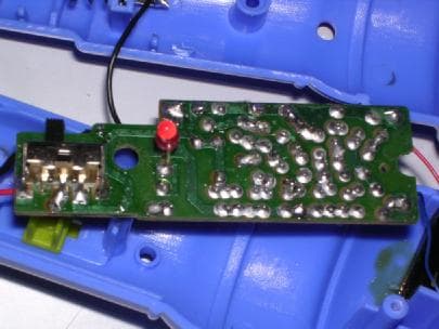
GAFMIC2
Aug 01, 2004Wireless Microphone
Equipment Class
DXX - Part 15 Low Power Communication Device Transmitter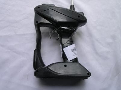
GAFRC16FF27
Jun 29, 2004Remote Control Toy Transmitter
Equipment Class
DXX - Part 15 Low Power Communication Device Transmitter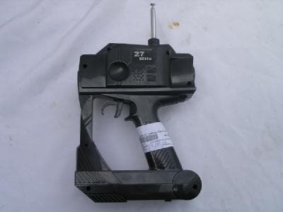
GAFRC16SM27
Jun 06, 2004Remote Control Toy Transmitter
Equipment Class
DXX - Part 15 Low Power Communication Device Transmitter
GAFWT-SD2
Oct 06, 2003Walkie Talkie
Equipment Class
DXX - Part 15 Low Power Communication Device Transmitter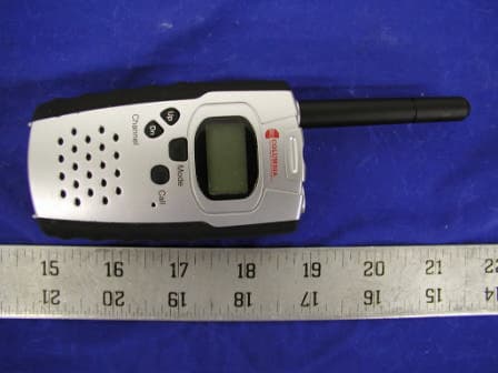
GAFGM18
May 28, 2003GMRS/FRS 2-Way Radio
Equipment Class
TNF - Licensed Non-Broadcast Transmitter Held to Face