HYQBTA01ABluetooth ASSY.
Denso Corporation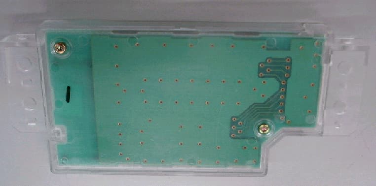
Click to zoom
Application Details
- Equipment Class
- DSS - Part 15 Spread Spectrum Transmitter
- Date of Grant
- Mar 27, 2003
- Application Purpose
- Original Equipment
- Date of Application
- Mar 25, 2003
- Equipment Note
- Bluetooth ASSY.
- Frequency Range
- 2402.00000000 - 2480.00000000
- Company
- Denso Corporation
- Country
- Japan
Documents & Files
Document Text
Text extracted from the exhibit documents filed with the FCC. Open a document above to read the original.
Users Manual
6.User’s manual requirement 6.1.Operation manual (1) Registration of the cellular phone Transmits the registration signal from the cellular phone to the navigation system and register the cellular phone at the navigation system. (2) Selection of the cellular phone Transmits the selection signal from the navigation system to the cellular phone and connect the navigation system with the cellular phone. (3) Call Call by inputting the phone number with the touch sensitive panel installed in the navigation system. Get the phone by operating the touch sensitive panel installed in the navigation system. Bluetooth RF signal Bluetooth RF signal Bluetooth RF signal Cellular RF signal 6.2.User’s Manual Requirement of FCC rule BTA-01A is installed in the navigation system, so BTA-01A has no manual for user. FCC user’s manual requirements that are FCC rule Part 15.21 and 15.105 are described on user’s manual of the vehicle. Fig 6.2. FCC rule requirement for user’s manual FCC and RSS-210 Regulations This device complies with Part 15of the FCC Rules and RSS-210 Rules Operation is subject to the following two conditions : (1) this device may not cause harmful interference, and (2) this device must accept any interference received, including interference that may cause undesired operation. FCC WARNING : Changes or modifications not expressly approved by the party responsible for compliance could void the user’s authority to operate the equipment.
External Photos
DENSO CORPORATION Bluetooth ASSY FCC ID: HYQBTA01A (External Photos) Component side DENSO CORPORATION Bluetooth ASSY FCC ID: HYQBTA01A Solder side
ID Label/Location Info
4.5. Appearance and FCC and IC Label Location of Bluetooth ASSY 4.5.1. Appearance Fig. 4.5.1. Photo of Bluetooth ASSY PCB Layout RF Shield 4.5.2. FCC and IC Label location of Bluetooth ASSY Fig. 4.5.2. Label Location on Bluetooth ASSY 4.5.3. Label Layout on Bluetooth ASSY Unit : mm Fig. 4.5.3. Label Layout Note : Compliance statement of marking will not be changed. But marking layout and size maybe changed. Stick the Yupo paer label on the plastic case. (23) (39) 4.6.1. FCC and IC ID Label layout and location on Navigation ASSY Front view Rear view Fig. 4.6.1. FCC and IC Label Location on Navigation ASSY 4.6.2. FCC and IC ID Label on Navigation ASSY Unit : mm Fig. 4.6.2. FCC and IC ID Label layout Note : Compliance statement of marking will not be changed. But marking layout and size maybe changed. Stick the Yupo paper label on the matal case. (15) (30) Contains: MODEL:BTA-01A FCC ID:HYQBTA01A IC ID:1551A-BTA01A
Internal Photos
DENSO CORPORATION Bluetooth ASSY FCC ID: HYQBTA01A (Internal photo) Bluetooth module IC DENSO CORPORATION Bluetooth ASSY FCC ID: HYQBTA01A Bluetooth module IC (Component side) DENSO CORPORATION Bluetooth ASSY FCC ID: HYQBTA01A Bluetooth module IC (Solder side)
Operational Description
FCC ID: HYQBTA01A Additional information in accordance with requirements of FCC 15.247 and FCC Public Notice DA 00-705 1. Frequencies tested Frequencies for the test are 2402 MHz, 2441 MHz and 2480 MHz as specified in 15.31(m). 2. Antenna requirement The Bluetooth transceivers are used for data transmission between handy phone and navigator system. The antenna is a chip antenna and is permanently mounted on a printed electronic circuit board of this module. In addition, since the module is installed in the display of navigator system by OEM’s’ (professional installers), it is impossible for end user to replace it. This antenna configuration complies with the requirement of FCC 15.203. The gain of antenna used is –5 dBi or more (less than 6 dBi). 3. AC conducted noise N/A (DC Operation) 4. Carrier frequency separation The measurement is carried out in accordance with FCC Public Notice DA 00-705 and the compliance is reported in the test report. 5. Hopping frequency requirements The number of hopping frequencies is measured in accordance with FCC Public Notice DA 00-705 and reported the compliance in the test report. On pseudorandom frequency hopping sequence the following is an example of a 79 hopping sequence in data transmission mode: 52, 35, 50, 20, 54, 67, 56, 37, 60, 39, 58, 69, 62, 71, 64, 25, 68, 27, 66, 57, 70, 59, 72, 29, 76, 31, 74, 61, 78, 63, 01, 41, 05, 43, 03, 73, 07, 75, 09, 45, 13, 47, 11, 77, 15, 00, 16, 49, 28, 22, 34, 02, 19, 06, 17, 51, 32, 36, 14, 04, 12, 26, 18, 24, 38, 08, 30, 65, 10,40, 21, 44, 23, 42, 53, 46, 55, 48, 33 Example of a hopping sequence in inquiry mode: 55, 59, 10, 73, 65, 69, 43, 27, 00, 77, 04, 67, 37, 06, 31, 75, 33, 39, 51, 29, 40, 14, 35, 49, 47, 08, 71, 63, 57, 02, 61, 45 Example of a hopping sequence in paging mode: 61, 44, 46, 63, 14, 50, 48, 16, 65, 52, 54, 67, 18, 58, 56, 20, 53, 60, 62, 55, 06, 66, 64, 08, 57, 68, 70, 51, 02, 42, 40, 04 The requirement of equal hopping frequency use is met by a unique generation of the hopping sequence specified in the Bluetooth Standard as follows; The generation of the hopping sequence in connection mode depends essentially on two input values: 1. LAP/UAP of the master of the connection 2. Internal master clock The LAP (lower address part) are the 24 LSB’s of the 48 BD_ADDRESS. The BD_ADDRESS is an unambiguous number of every Bluetooth unit. The UAP (upper address part) are the 24 MSB’s of the 48 BD_ADDRESS. The internal clock of a Bluetooth unit is derived from a free running clock which is never adjusted and is never turned off. For synchronization with other units only offset are used. It has no relation to the time of the day. Its resolution is at least half the RX/TX slot length of 312.5 us. The clock has a cycle of about one day (23 hours and half). In most case it is implemented as 28 bits counter. For the deriving of the hopping sequence the entire LAP (24 bits), 4 LSB’s (4 bits) (Input 1) and the 27 MSB’s of the clock (Input 2) are used. With this input values different mathematical procedures (permutations, additions and XOR-operations) are performed to generate the sequence. This will be done at the beginning of every new transmission. Regarding short transmissions the Bluetooth system has the following behavior; The first connection between the two devices is established, a hopping sequence was generated. For transmitting the wanted data the complete hopping sequence was not used. The connection ended. The second connection is established. A new hopping sequence is generated. Due to the fact that the Bluetooth clock has a different value, because the period between the two transmission is longer than the minimum resolution of the clock (312.5 us). The hopping sequence always differs from the first one. For the generation of the inquiry and page hop sequences the same procedures as described above, but this time with different input vectors. For the inquiry hop sequence, a predefined fixed address is always used. This results on the same 32 frequencies used by all devices doing an inquiry but every time with a different start frequency and phase in this sequence. For the page hop sequence, the device address of the paged unit is used as input vector. This results in the use of a subset of 32 frequencies which is specific for that initial state of the connection establishment between the two units. A page to different devices would result in a different subset of 32 frequencies. 6. Dwell time Dwell times are measured in accordance with FCC Public Notice DA 00-705 and reported in the test report. 7. 20 dB bandwidth The 20 dB bandwidth is measured in accordance with FCC Public Notice DA 00-705 and reported the compliance in the test report. 8. Receiver input bandwidth and hopping capability The input bandwidth of the receiver is limited to 1 MHz by a bandpass filter at the IF stage. It complies with the transmitter bandwidth at each hopping frequency. In every connection one Bluetooth device is the master and the other one is the slave. The master determines the hopping sequence. The slave follows this sequence. Both devices shift between RX and TX time slot according to the clock of the master. Additionally the type of connection is set up at the beginning of the connection. The master adapts its hopping frequency and its TX/RX timing according to the packet type of the connection. Also the slave of the connection uses these settings. Repeating of a packet has no influence on the hopping sequence. The hopping sequence generated by the master of the connection is followed in any case. That means, a repeated packet is not sent on the same frequency, it is sent on the next frequency of the hopping sequence. 9. Peak output power The peak output power is measured in accordance with FCC Public Notice DA 00-705 and reported the compliance in the test report. 10. Defact EIRP limit The gain of antenna used in BTA-01A is –5 dBi or more (less than 6 dBi). There is no necessity to consider the defact EIRP li…
Text truncated - open the document above for the full version.
Operational Description
1. Product Outline The BTA-01A is the 2.4 GHz wireless LAN transceiver module which uses frequency hopping spread spectrum technology in accordance with the Bluetooth Specification version1.1. This product is installed only in some specified navigation systems. This product connects the navigation system with the cellular phone by radio. The navigation system enables the driver to call without holding the cellular phone by using speaker, microphone and touch sensitive panel installed in the system. This application is called "hands free”. 2. Specification of Product - Product name : Bluetooth ASSY - Standard based upon : Bluetooth Spec. Ver.1.1 - Product Type No. : BTA-01A - Frequency range : 2402MHz to 2480MHz - Output power : 1mW (0dBm) - Nominal voltage : 3.3 ± 0.2 VDC 4.2. Component Layout of Bluetooth ASSY All parts are mounted in the component side and there are no parts in the solder side. Scale : Fee Fig. 4. Component layout (Component side) 5.4. Parts list of Bluetooth module IC Ref. No. Name Specification C2 Capacitor Open – 0.1ìF C4 Capacitor Open – 1000pF C5 Capacitor Open – 1000pF C6 Capacitor 10 – 100pF C7 Capacitor Open – 0.1ìF C8 Capacitor Open – 1000pF C10 Capacitor Open – 1000pF C11 Capacitor 1000pF – 0.1ìF C12 Capacitor 1000pF – 0.1ìF C13 Capacitor Open – 1000pF C14 Capacitor Open – 1000pF C15 Capacitor Open – 1000pF C17 Capacitor 1 – 100pF C18 Capacitor 1 – 100pF C19 Capacitor Open – 10pF C20 Capacitor 100 – 1000pF C21 Capacitor 1000 – 0.01ìF C22 Capacitor 1 – 100pF C23 Capacitor Open – 10pF C24 Capacitor Open – 10pF C26 Capacitor Open – 1000pF C27 Capacitor 0.5 – 100pF C28 Capacitor 0.5 – 10pF C29 Capacitor Open – 0.1ìF C30 Capacitor Open – 0.1ìF C31 Capacitor 100pF – 0.1ìF C33 Capacitor Open – 0.1ìF C34 Capacitor 1 – 10ìF C35 Capacitor Open – 0.1ìF C37 Capacitor Open – 0.1ìF C40 Capacitor Open – 10pF C51 Capacitor Open – 1000pF C90 Capacitor 10 – 100pF C100 Capacitor Open – 1000pF C101 Capacitor Open – 1000pF C102 Capacitor Open – 1000pF C103 Capacitor Open – 1000pF C110 Capacitor 10 – 1000pF C112 Capacitor 1 – 100pF C113 Capacitor 1 – 100pF C114 Capacitor 1 – 100pF C115 Capacitor Open – 10pF C116 Capacitor Open – 100pF Ref. No. Name Specification R1 Resistor 100 ohm – 10 kilo ohm R3 Resistor 100 ohm– 10 kilo ohm R8 Resistor 1 – 10 kilo ohm R12 Resistor 1 – 100 kilo ohm R14 Resistor 1 – 10 kilo ohm R90 Resistor 100 ohm – 1 kilo ohm R92 Resistor 10 – 100 kilo ohm R93 Resistor 10 – 100 kilo ohm R94 Resistor 100 ohm – 10 kilo ohm R95 Resistor 100 ohm – 10 kilo ohm R96 Resistor 10 – 100 kilo ohm R97 Resistor 10 – 100 kilo ohm R98 Resistor 10 – 100 kilo ohm R101 Resistor 10 – 100 kilo ohm R102 Resistor 10 – 100 kilo ohm R104 Resistor 10 – 100 kilo ohm R105 Resistor 100 ohm – 10 kilo ohm R106 Resistor 100 ohm – 10 kilo ohm R107 Resistor 100 ohm – 10 kilo ohm R108 Resistor 100 ohm – 10 kilo ohm R109 Resistor 100 ohm – 10 kilo ohm L1 Inductor 1.0 – 3.3nH L2 Inductor 1.0 – 3.3nH L3 Inductor 10 – 22nH L4 Inductor 1 – 22nH L5 Inductor 1 – 22nH L6 Inductor 1 – 22nH L7 Inductor 1 – 22nH D1 Diode BAR64-05w F1 BPF MDR746F IC1 RF IC PMB6627XT IC2 Baseband IC PMB6752E IC4 EEPROM AT24C16N-10TI-2.5 IC5 Flash Memory SST39VF400A-70-4I-B3K TR1 Transistor 2SA1576A T106S X1 X’ Tal TSX-10A
Operational Description
6.3. Installation Description BTA-01A shall be installed in the navigation system as shown in Fig.6.3. When BTA-01A is installed in the navigation system, we as OEM shall consider the following points; 1. Since BTA-01A owns its FCC ID number, we shall affix an exterior label on the outside of the navigation system if the FCC ID is not visible. The exterior label shall use wording such as either “Contains Transmitter Module FCC ID: HYQBTA01A” or “Contains FCC ID: HYQBTA01A“. 2. BTA-01A complies with requirements of sub-sections 15.203, 15.205, 15.209 and 15.247 in FCC Rules Part 15. We shall install BTA-01A in accordance with their requirements. 3. BTA-01A complies with requirements of the sub-section 2.1091. When installers install BTA-01A into the navigator system, they shall ensure that the public is not exposed to radio frequency energy levels in excess of the Commission’s guidelines in accordance with the sub-section 15.247(b)(4) in FCC Rules Part 15. Fig. 6.3. Installation Description BTA-01A BTA-01A
RF Exposure Info
RF Exposure Statement No. : 23HE0018-HO-1 Applicant : DENSO CORPORATION Type of Equipment : Bluetooth ASSY Model No. : BTA-01A FCC ID : HYQBTA01A A-Pex International Co., Ltd. EMC Head Office Division. 4383-326 Asama-cho, Ise-shi, Mie-ken 516-0021 JAPAN Telephone : +81 596 24 8116 Facsimile : +81 596 24 8124 RF Exposure Statement: DENSO CORPORATION declares that Model : BTA-01A complies with FCC radiation exposure requirement specified in the FCC Rules 2.1093(2). BTA-01A has 0.83 mW of conducted Peak output power and 1.04 mW of EIRP.(Antenna gain : 1.0dBi) According to RF output power of this module transmitter, values for both Conducted peak output power and EIRP are below 5mW.This kind of equipment hardly ever go over SAR value limited of 1.6W/Kg for public resident which is regulated by "OET Bulletin65, Supplement C". RF Exposure Calculations: The following information provides the minimum separation distance for the highest gain antenna provided with the “BTA-01A” as calculated from FCC OET 65 Appendix B, Table (B) Limits for General Population / Uncontrolled Exposure. This calculation is based on the highest EIRP possible from the system, considering maximum power and antenna gain, and considering a 1.0m W/cm^2 uncontrolled exposure limit. The Friis formula used was: S = (P * G) / (4* p * r^2) or r = (P * G) / (4 * p* S) Where S = 1.0 mW/cm^2 for 2400 MHz P = 0.83mW (Maximum Conducted Power) G = 1.26 (Numerical Antenna gain; equal to 1.0 dBi) r = Minimum safe distance from antenna (cm) For: BTA-01A r = 0.29 cm Notes in Installation Manual: FCC Radiated Exposure Statement: This module may be installed into any end product both mobile and portable applications. Because the module only radiates very low power levels, it complies with RF exposure requirements. According to Supplement C, Edition 01-01 to OET Bulletin 65, Edition 97-01 spread spectrum transmitters are categorically excluded from routine environmental evaluation because of the low power level, where there is a high likelihood of compliance with RF exposure standards.
Test Report
Test report No. : 23HE0018-HO-1 Page : 2 of 47 Issued date : March 14, 2003 FCC ID : HYQBTA01A A-Pex International Co., Ltd. EMC Head Office Division. 4383-326 Asama-cho, Ise-shi, Mie-ken 516-0021 JAPAN Telephone: +81 596 24 8116 Facsimile: +81 596 24 8124 CONTENTS PAGE SECTION 1: Client information 3 SECTION 2: Equipment under test (E.U.T.) 3 SECTION 3: Test specification, procedures and results 5 SECTION 4: Operation of E.U.T. during testing 7 SECTION 5: Carrier Frequency Separation, Section 15.247 (a)(1) 8 SECTION 6: 20dB Bandwidth, Section 15.247(a)(1) 8 SECTION 7: Number of Hopping Frequency, Section 15.247(a)(1)(iii) 8 SECTION 8: Dwell time, Section 15.247(a)(1)(iii) 8 SECTION 9: Maximum Peak Output Power, Section 15.247(b)(1) 8 SECTION 10: Band Edge Compliance, Section 15.247(c) 9 SECTION 11: Spurious Emission, Section 15.247(c) 9 APPENDIX 1: Photographs of test setup 10 APPENDIX 2: Test instruments 10 APPENDIX 3: Data of EMI test 10 Test report No. : 23HE0018-HO-1 Page : 3 of 47 Issued date : March 14, 2003 FCC ID : HYQBTA01A A-Pex International Co., Ltd. EMC Head Office Division. 4383-326 Asama-cho, Ise-shi, Mie-ken 516-0021 JAPAN Telephone: +81 596 24 8116 Facsimile: +81 596 24 8124 SECTION 1: Client information Company Name : DENSO CORPORATION Brand Name : DENSO Address : 1-1 Showa-cho, Kariya-shi, Aichi-ken, 448-8661 Japan Telephone Number : +81-566-61-3711 Facsimile Number : +81-566-25-4941 Contact Person : Hiroshi Miyazaki SECTION 2: Equipment under test (E.U.T.) 2.1 Identification of E.U.T. Type of Equipment : Bluetooth ASSY Model No. : BTA-01A Serial No. : 23, 40 Rating : DC3.3V DC5V Country of Manufacture : Japan Receipt Date of Sample : March 5, 2003 Condition of EUT : Production prototype Test report No. : 23HE0018-HO-1 Page : 4 of 47 Issued date : March 14, 2003 FCC ID : HYQBTA01A A-Pex International Co., Ltd. EMC Head Office Division. 4383-326 Asama-cho, Ise-shi, Mie-ken 516-0021 JAPAN Telephone: +81 596 24 8116 Facsimile: +81 596 24 8124 2.2 Product Description Model: BTA-01A which was referred to as the EUT in this report is a Bluetooth ASSY. This product is installed in Display in a Navigation system. And this product is used for a Hands free system. Instead of having connected using the cable, a Navigation system is connected with a cellular phone on radio by using this product. The specification is as following; Equipment Type : Transceiver Clock frequency used in EUT : 13MHz Frequency characteristics : from 2402MHz to 2480MHz Type of modulation : GFSK Bandwidth & Channel spacing : 78MHz, 1MHz Emission Designation (ITU Code) : F1D Antenna Type : λ/ 4 Uni-pole Antenna Connector type : MM8430-2600B Antenna gain : 1.0dBi (Max) Method of Frequency Generation : ■ Crystal ■ Synthesizer □ Other (Resonator) Power Supply : DC3.3V Operating voltage : DC3.1-3.5V Duty cycle : 0.78 Operating temperature : -30deg.C. to+85deg.C. Power & Signal Cable Length : □ > 3m ■ ≤ 3m *FCC Part 15.31(e) Verification of Input Power: The host device BTA-01A provide the stable power-supply (DC 3.3V); and the Bluetooth ASSY complies power supply regulation. *FCC Part 15.203 Antenna requirement The antenna built in the BTA-01A is a chip antenna and is permanently mounted by soldering on a printed electronic circuit board in BTA-01A. It is impossible for end users to replace it, because a special tool is necessary for removal of the antenna. Test report No. : 23HE0018-HO-1 Page : 5 of 47 Issued date : March 14, 2003 FCC ID : HYQBTA01A A-Pex International Co., Ltd. EMC Head Office Division. 4383-326 Asama-cho, Ise-shi, Mie-ken 516-0021 JAPAN Telephone: +81 596 24 8116 Facsimile: +81 596 24 8124 SECTION 3: Test specification, procedures and results 3.1 Test Specification Test Specification : FCC Part 15 Subpart C and Section15.247 Title : FCC 47CFR Part15 Radio Frequency Device Subpart C Intentional Radiators Section 15.247 Operation within the bands 902-928MHz, 2400-2483.5MHz, 5725-5850MHz 3.2 Procedures and results No. Item Test Procedure Specification Remarks Deviation Worst margin Results 1 Conducted Emission ANSI C63.4:2001 Section 15.207 N/A Excluded * N/A Complied 2 Carrier Frequency Separation ANSI C63.4:2001 Section15.247(a)(1) Conducted N/A N/A Complied 3 20dB Bandwidth ANSI C63.4:2001 Section15.247(a)(1) Conducted N/A N/A Complied 4 Number of Hopping Frequency ANSI C63.4:2001 Section15.247(a)(1)(iii) Conducted N/A N/A Complied 5 Dwell time ANSI C63.4:2001 Section15.247(a)(1)(iii) Conducted N/A N/A Complied 6 Maximum Peak Output Power ANSI C63.4:2001 Section15.247(b)(1) Conducted N/A N/A Complied 7 Band Edge Compliance ANSI C63.4:2001 Section15.247(c) Conducted N/A N/A Complied 8 Spurious Emission ANSI C63.4:2001 Section15.247(c) Conducted/ Radiated N/A 5.8dB 223.20MHz Horizontal/ Vertical Complied * The test is not applicable since the EUT does not have possibility to be connected with the AC Power. These tests were performed without any deviations from test procedure except for additions or exclusions. 3.3 Confirmation A-Pex International Co., Ltd. hereby confirms that E.U.T. , in the configuration tested, complies with the specifications FCC Part15 Subpart C Section 15.247. 3.4 Uncertainty Spurious Emission(Radiated) The measurement uncertainty (with a 95% confidence level) for this test using Biconical antenna is + 4.5dB. The measurement uncertainty (with a 95% confidence level) for this test using Logperiodic antenna is + 5.2dB. The measurement uncertainty (with a 95% confidence level) for this test using Horn antenna is + 6.6dB. The data listed in this test report may exceed the test limit because it does not have enough margin. Other test except Conducted Emission and Spurious Emission(Radiated) The measurement uncertainty (with a 95% confidence level) for this test was + 3.0dB. The data listed in this test report has enough margin. Test report No. : 23HE0018-HO-1 Page : 6 of 47 Issued date : March 14, 2003 FCC ID : HYQBTA01A A-Pex International Co., Ltd. EMC Head Office Division.…
Text truncated - open the document above for the full version.
Test Setup Photos
Test report No. : 23HE0018-HO-1 Page : 11 of 47 Issued date : March 14, 2003 FCC ID : HYQBTA01A A-Pex International Co., Ltd. EMC Head Office Division. 4383-326 Asama-cho, Ise-shi, Mie-ken 516-0021 JAPAN Telephone: +81 596 24 8116 Facsimile: +81 596 24 8124 APPENDIX 1: Photographs of test setup Spurious Emission (Radiated) Test report No. : 23HE0018-HO-1 Page : 12 of 47 Issued date : March 14, 2003 FCC ID : HYQBTA01A A-Pex International Co., Ltd. EMC Head Office Division. 4383-326 Asama-cho, Ise-shi, Mie-ken 516-0021 JAPAN Telephone: +81 596 24 8116 Facsimile: +81 596 24 8124 Other tests except Conducted emission and Spurious Emission (Radiated)
Contact Information
Applicant
Keijiro Kumagai(Manager)
Technical Contact
A-Pex International Co., Ltd.Hiroka Umeyama
[email protected]+81-596-24-8116
4383-326 Asama-cho · Ise-shi, Mie-ken · Japan
Test Firm
UL Japan, IncMitsuru Fujimura
Technical Specifications
| # | Rule Parts | Frequency Range | Power Output |
|---|---|---|---|
| 1 | 15C | 2.40 GHz - 2.48 GHz | 830.00 µW |
Other Applications from Denso Corporation
HYQDNILR001
Aug 04, 2026LiDsEYE
Equipment Class
JAB - Part 15 Class B Digital DeviceHYQDNMWR020
Mar 27, 2026Millimeter Wave Radar Sensor
Equipment Class
VRD - Part 95 Vehicular Radar SystemsHYQDNMWR021
Mar 10, 2026Millimeter Wave Radar Sensor
Equipment Class
VRD - Part 95 Vehicular Radar SystemsHYQ23ABR
Mar 05, 2026Remote Keyless Entry System and TPMS (Receiver)
Equipment Class
CYY - Communications Receiver used w/Pt 15 TransmitterHYQDNMWR018RAM
Oct 10, 2024Millimeter Wave Radar Sensor
Equipment Class
VRD - Part 95 Vehicular Radar Systems